
Chapter 8
Reconfigurable Printed Antennas1
8.1. Introduction
The telecommunication domain in recent years has seen incredible growth. Over the years, downsizing of mobile systems in particular has led to the design of increasingly miniature antennas, responding to severe radio-electric constraints. Nowadays, higher transmission rates and the ever increasing number of wireless communication devices and standards require antennas with the capability to answer to additional features which are often impossible to obtain using conventional radiating structures. Thus, to quickly match to a changing channel frequency (cognitive radio) or random environment, reconfigurable antenna design becomes a necessity. The most commonly desired objectives are generally of course the automatic adjustment of frequency but sometimes, also the real-time correction of radiation pattern or polarization direction.
Research on so-called active antennas, conducted initially in an effort to reduce noise and losses in the transmission lines between the antenna and the RF circuits, have thus migrated over time from a lot of various electronic functions such as frequency mixing, oscillation, modulation [CHA 02], to more recently, frequency, radiation pattern or polarization dynamic reconfiguration. Indeed, many academic and industrial researchers have investigated the possibility of dynamically changing the radio-electric characteristics of an antenna. Solutions have been proposed for many types of radiating elements. However, due to the nature of the field, this chapter presents only illustrative examples of some possible solutions based on reconfigurable printed or planar antennas [JAM 89].
8.2. Active antennas
The dynamic reconfiguration of an antenna is usually performed using one or more active electronic components (varactor or PIN diodes, transistors, MEMS, etc.), integrated within the radiating structure. That is why the concept of a reconfigurable antenna is generally closely linked to the notion of an active antenna. The term active antenna is not yet universally recognized and several interpretations exist. Once an antenna has realized an active function of the RF signal before emitting or after receiving, it can be considered an active antenna. The ambiguity of this definition implies that most of the antennas can be called active if active devices involved in the wireless transmission are relatively close to the radiating element, such as on the same substrate or at a distance lower than the near field limit. A reconfigurable antenna can be distinguished however from an active antenna by the fact that the own radio-electric characteristics of the antenna can be modified by the active part, and that the latter does not realize “simple” operations such as amplification or filtering [ITO 97].
8.3. Active components used for reconfiguration
A lot of active electronic components can be used to make an antenna active [NAV 92]. For example, [KWO 79] showed the use of a Barritt diode in a printed antenna structure type in the late 1970s. In the 1980s, some works proposed Impatt or Gunn diodes [PER 86, PER 87, YOU 87] but also more recently in [KAN 08]. Field effect transistors (FET), because of their interesting properties have also been proposed as RF switching or amplification elements.
More recently, many studies have shown the potential of RF MEMS (Micro Electro Mechanical Systems) in the field of antennas [PET 79, MON 06, PAN 06a, PAN 06b, FER 07b]. Coming from the microelectronics domain, these electromechanical devices have particularly attractive advantages such as a very low consumption, high isolation in the off-state and small losses. However, actuation voltage and switching time are generally considered as the main drawbacks. In the case of frequencies within the band of 50 to 100 GHz, an alternative is the use of systems integrating simultaneously radiating elements and active circuits within a single chip (antenna on chip — AOC). However, the two active components often found in RF reconfiguration studies are certainly the varactor and the PIN diodes [BAH 88, CAR 01]. In this chapter, these two components, especially widespread in recent years in active microstrip antennas, are described a little more in detail and simple electrical circuit models are proposed. Indeed, different methods — transmission line, integral equation, moment method — can be used to model the radio-electric influence of the active components and to predict the behavior of the antenna.
The transmission lines model, where the antenna is considered as a microstrip line loaded at both ends, allows us to take into account the active devices by the integration of simple associated electrical circuits in different locations of the equivalent transmission line fairly easily [JAM 89, TUR 01]. The transmission line model is then very useful for a comprehensive approach of physical phenomena and the method was improved since the original model. However, due to the complexity of modern radiating elements, coupled with the effects that active components can create in terms of surface currents and internal coupling on the structure, more efficient simulators can be used today. In spite of these powerful CAD tools, final results often have to be fine tuned experimentally.
8.3.1. The varactor diode
The varactor diode is one of the most active components used to realize a continuous frequency control of a printed antenna [BHA 82, WAT 92] because its use is based on the historical concept of the variable tuning capacitor for adjusting the frequency operation of a resonating system. Modeling the electrical behavior of the varactor diode can be made in a first approximation, for example by one of the two equivalent electrical lumped element models presented in Figure 8.1. Other models can be found in the literature depending also on whether the diode is considered to be either packaged or not [BAH 88].
Figure 8.1. Equivalent electrical circuits of a varactor diode
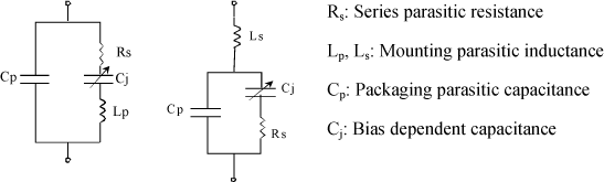
By increasing the reverse voltage across the diode, the value of the variable capacitance Cj decreases. However, this relationship is nonlinear. The range of variation of the classically used solid-state diodes is in the order of 10 to 1 pf, for a length of the device approximately equal to 1 mm. One of the major drawbacks of the varactor diode is that it can cause a strong decrease in the total efficiency and gain of the antenna. An important part of the energy delivered to the loaded antenna is not radiated, but dissipated by ohmic losses. It is important therefore to have diodes with very low internal resistances Rs, to limit their number within a single structure and to find the best possible trade-off between voltage and current values on the structure for their placement.
8.3.2. The PIN diode
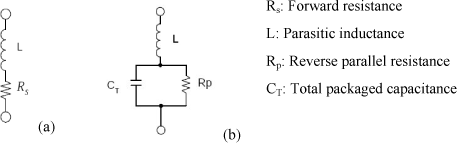
The PIN diode is one of the most common components in RF switching circuits and active antennas, as its switching time is very short. The two operating states, closed (a) and open (b), can be represented respectively by the following equivalent circuits (Figure 8.2) [FER 07]. Again, other models can be found in the literature [BAH 88].
Figure 8.2. Simplified electrical equivalent circuit of a PIN diode: (a) forward bias (b) reverse bias
8.4. Printed antennas and compact antennas
The generic printed antenna is a partial metallization, historically of simple shape (square, rectangle, disk, etc.), laid on the upper surface of an insulated dielectric substrate, having itself a continuous metal layer on its opposite side usually called a ground plane [JAM 89, LUX 07]. The radiating upper metallization, which can nowadays take a lot of various and different shapes, strongly influences operation type and performance of the antenna. Generally, the dimensions of the radiating part are about half the wavelength and the metallization is realized in very good conductors such as copper, silver or gold. Dielectric substrate characteristics also greatly influence the behavior of the antenna. We generally select a low dielectric thickness compared to the wavelength used (a few tenths of λ). Ideally, the relative permittivity εr of the substrate and its loss parameter tanδ must be quite low. When air is used as substrate, the planar antenna consists of a piece of metallic sheet, most often supported by dielectric spacers or by some material as low loss dielectric foam or honeycomb.
The feeding of these antennas can be done in different ways, often dictated by the application. We thus distinguished:
– for the coaxial probe, between metallic strip, microstrip line or printed coplanar waveguide on the same layer as the radiating element;
– for coupling between the coupling through a slot in the ground plane or the proximity coupling.
If planar antennas generally prefer the coaxial probe or the vertical metallic strip feed enabling us to simultaneously support the upper metallic plate radiating element, microstrip antennas generally use lines of the same name, and therefore the same technology. The feeding choice also determines how the active components can be implemented and therefore also the reconfiguration mode.
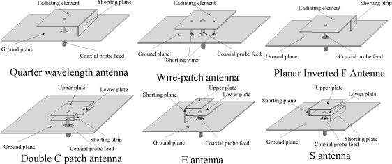
The reconfiguration of an antenna is often employed to compensate for a decrease in antenna performance due to its miniaturization, especially in terms of bandwidth. Miniature antennas were the focus of many studies, both for their properties of compactness, but now also to involve the reconfiguration, especially for applications in the field of mobile telephony [FUJ 87]. The antennas are generally called compact or small, if their dimensions do not exceed a quarter of a wavelength. Inverted antennas fall into this category, but there are many other types of compact antennas: L, F, C, E, double C, etc. antennas (Figure 8.3) [CAR 01]. Their names are based on the particular shape of these elements. Another important property of antennas with ground-wires or short-circuit strips is their radiation patterns enabling them to receive horizontal and/or vertical polarized waves. This characteristic of radiation appears to be very useful in an urban environment for example, where the electromagnetic fields may fluctuate in amplitude but also in polarization direction. These antennas, including the PIFA (planar inverted F antenna) have been exploited in many forms in the field of mobile telephony [CAR 01].
Figure 8.3. Different types of miniature antennas
8.5. Frequency reconfigurable antennas
Printed antennas inherently presenting narrow bandwidths are naturally good candidates for frequency reconfiguration and the number of publications in this field has increased significantly since the 1990s. Generally two types of reconfiguration can be distinguished, continuous and switching/hopping.
8.5.1. Continuous frequency reconfiguration
8.5.1.1. Printed and compact antennas
Few particular works such as those involving the integration under the patch element of a resistor and a capacitor [LU 98] can be found in the literature. By varying the resistance or capacity, the authors succeed in decreasing the resonant frequency while increasing the bandwidth. However, since the well-known publication in the 1980s by Bhartia and Bahl presenting a microstrip antenna integrating two varactor diodes [BHA 82], the solution of replacing the capacity by a voltage-controlled varactor diode has been preferred by many authors.
In this case, the principle of controlling the printed antenna is the following: by placing at least one varactor diode between the ground plane and the radiating part [ABE 92], an additional shunt capacitance load is added, which can also be introduced in the RLC equivalent model defined at the resonant frequency of the patch [BHA 82]. By changing this capacitance, the resonant frequency is thereby modified.
The main problem of this solution is then to continuously maintain the matching during the frequency change because the input impedance is also a function of the equivalent RLC model component values and fringing effects. Therefore, feeding based on coupling (slot in the ground plane, proximity coupling) is generally preferred rather than direct injection current as in the case of direct feeding by a microstrip line connected to the patch or a coaxial probe feed, because matching can be better preserved. However, coaxial probe feed (or vertical metallic strip feed) is generally retained for mobile phone antennas for which other reconfiguration solutions, including several diodes have emerged.
Another example consists of an asymmetric dipole loaded by a varactor diode (Figure 8.4). This antenna [CAR 01] is an example of a radiating coaxial probe feed element that can integrate an active element without significant modifications in its geometry. This is an air-substrate antenna with small dimensions.
Figure 8.4. Asymmetric C dipole loaded by a varactor diode
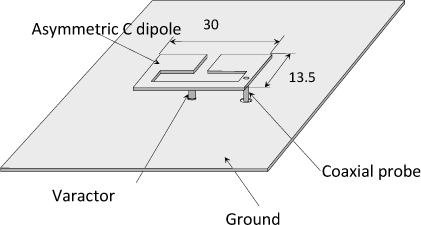
Figure 8.5. Frequency shift versus reverse DC bias voltage
To obtain a significant influence on the antenna behavior with the added capacitive effect, it is generally necessary to insert the varactor diode where electric fields are high, and surface currents are low. This point is difficult to find for the first mode. However, it naturally exists for the second mode, on the symmetry axis of the antenna. Then, the antenna is not matched as the varactor diode is not biased by a reverse voltage, which is also a way of enabling or not the functioning of the structure. A voltage of about 10 volts allows the matching of the antenna from a frequency of 2.6 GHz (Figure 8.5). A shift of this frequency up to 3.5 GHz can be obtained when using different reverse bias voltages. This solution allows a frequency bandwidth of 50 MHz without any mismatching over the entire reconfiguration frequency band, which is also often the most difficult point to obtain in frequency reconfiguration.
Varactor diodes can also be used on various monopole antenna types or printed dipoles [KOL 98]. A serial insertion of a diode in a metallic part of the radiating element is able to create a change in the capacitive load, allowing a longer total electrical equivalent length. This capacitive effect can also change the resonant frequency of printed slots. In this case, the insertion of a variable capacity on a straight, an annular or a square ring radiating slot also allows a frequency reconfiguration. Open slots realized in radiating elements loaded by an active device can also be used to obtain a frequency reconfiguration of the fundamental resonant frequency but more generally also on higher modes of the antenna.
8.5.1.2. Compact antennas with shorting pins
Insertion of varactor diodes in the case of coaxial probe fed elements is unconstrained as long as no short-circuit or metallic part is connected between the radiator and the ground plane. Indeed, in this case the entire structure (radiating element, probe and ground plane) is at the same DC electrical potential, which makes the biasing of the active components difficult. Ground wire antennas are however very interesting, because they allow us to reduce the size of the structure before reconfiguration. Works in this area are presented in [PAN 01] on a PIFA type antenna. In this study, an additional capacitor is added to optimize the frequency range.
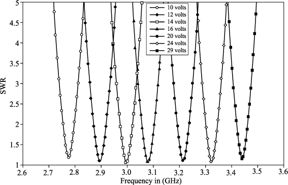
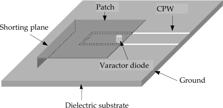
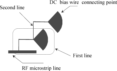
To overcome the problems of DC bias in the case of short-circuited antennas, decoupling can be obtained using capacitive slots realized in the ground plane, all around the metallic shorting parts. RF coupling can be enhanced, for instance, using additive capacitors across these slots. Another solution consists of replacing the coaxial type excitation by a coplanar waveguide (CPW) which offers the advantage of allowing both the insertion of varactor diodes and their DC biasing [CAR 01] [TUR 01]. Figure 8.6 shows the insertion of the active element. Its position was chosen to obtain an optimal return loss coefficient. The DC voltage required for the polarization of the diode is superimposed on to the microwave signal feeding the antenna through the coplanar waveguide [TUR 01].
Figure 8.6. CPW-fed frequency agile shorted patch controlled by a varactor diode
The antenna has an initial resonant frequency of 4.74 GHz and a bandwidth of 137 MHz (2.8%). After connecting the diode, the resonant frequency decreases to 4.19 GHz. The polarization of the diode with a DC voltage up to 25 volts provides a frequency shift of 317 MHz (7.3%) with a bandwidth of 70 MHz.
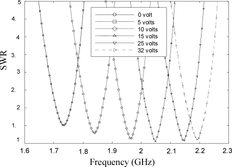
In these varactor-based solutions, the position of the diode and the width of the metallic part of the antenna receiving this diode are two important criteria for an efficient reconfiguration on a wide frequency band. The width of the metallic part, but also the height of the radiator where the diode is connected, determine the magnitude of the capacitive effect created, and therefore the electric field. The following example (Figure 8.7), which is based on an S-type antenna (Figure 8.3), shows the importance of optimization of the radiating element at the diode connecting point [CAR 01]. This S antenna is basically a dual-frequency antenna, operating around 1.82 GHz and 2.16 GHz for the given dimensions. It has a wide enough bandwidth to allow the coverage of PCS, DCS 1800 and UMTS standards. The S-type element is centered both on the slot and the CPW line, and the first height is adjusted to the length of the packaged diode. If the same diode is inserted in the original S-type antenna (Figure 8.3) between the central strip of the waveguide and the lower plate, its effect is not sufficient enough to get to a dynamic frequency reconfiguration. Indeed, it is placed in the center of an oversized metallic part to obtain a sensitive relative capacitive effect. It is therefore necessary to reduce the width of this lower metallic strip to the same size as the diode (1 mm). However, the width of the upper plate is also important. It determines the lower bound and the width of the frequency reconfiguration range. By enlarging the width of the upper plate, it would increase the useful frequency band. The antenna presented in Figure 8.7 is then optimized to cover the different standards. The frequency reconfiguration obtained covers a frequency range from 1.7 GHz to 2.23 GHz with a constant bandwidth of 60 MHz (Figure 8.8) and the final size of the antenna is then very small.
Figure 8.7. S antenna fed by a CPW line and controlled by a varactor diode
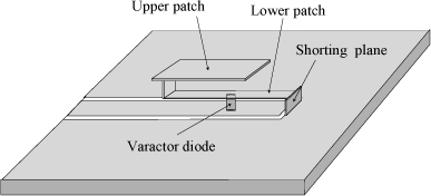
Figure 8.8. Frequency shift versus reverse DC bias voltage
8.5.2. Frequency hopping reconfiguration
A component with a switching function is typically used in the frequency hopping reconfiguration to electrically add or remove metallic parts in the antenna, shorten or lengthen the current path, thereby changing the electrical equivalent lengths. The components used in switching must therefore have two well-defined states which are generally short and open circuit states. In practice, both states are fairly well obtained by using semiconductor components such as PIN diodes or field effect transistors. The number of switching elements generally determines the number of possible frequencies. These components are also sometimes used at stub ends to bring at the entrance level of the antenna a specific desired impedance and then to directly realize the reconfiguration in terms of antenna input impedance matching or used in SPDT to switch between different tuning circuits interconnected through a pin to the antenna [KIV 02]. These switching elements may also be used in compact structures. In [SHY 05], a dual frequency behavior within a patch-type radiating element obtained by slot switching is presented. These switching components may also be introduced within the radiating element between the metallization and the ground plane in order to locally modify the distribution of fields and currents.
In 1980, Schaubert et al. [SCH 80] showed that the operating frequency of a patch antenna can be controlled by inserting shorting posts in different locations within the antenna and that by using RF switched diodes as tuning posts, an electronically tuned frequency agile antenna could be obtained. In [CHE 03], a PIN diode placed at the end of PIFA allows dual frequency operation. DC bias decoupling is obtained by inserting a capacitance between the shorting metallic strip and the ground plane. Due to this shorting strip, the antenna works as a PIFA when the PIN diode is in OFF-state while it operates as a loop antenna when the diode is in the the OFF-state. In [FEL 07], a PIFA type antenna is also made reconfigurable by the choice of shorting to the ground plane one of several straps cut in the grounded side. PIN diodes are also used to reduce the length of a resonant slot used as an antenna [LAH 01], or used as a coupling element to feed a square patch [LUX 00]. Reconfiguration based on frequency hopping has also been considered using MEMS switches, used for short-circuiting slots realized on the radiating elements to change the resonant modes [PAN 06a], or to add metallic parts and modify the path length of the currents [PAN 06b].
8.6. Radiation pattern reconfiguration
8.6.1. Printed arrays
One of the most common techniques used to obtain a reconfigurable radiation pattern consists of associating several radiating elements through a common power divider network. These antenna arrays, whether for detection or telecommunication systems, require an electronic control of the phase and the amplitude of the supply current on each element. This weighting allows a quick non-mechanical orientation of the main direction of radiation. The antenna array then allows more advanced applications such as continuous tracking of a target, restricting pursuit to limited angular sectors, research and tracking of multiple targets, etc. The obtained beam width depends on the number and the spacing of elements, and the pointing accuracy depends on the accuracy of the phase and amplitude laws that can be achieved through the feeding network. Printed antennas may be easily associated in arrays because of their printed circuit-type technology. The feeding network made in the same technology can be etched on the same surface as the radiating element but also on an intermediate layer between the radiator and the ground plane, or even behind the ground plane which is then common both to the radiating element and the feeding network. The feeding is thus performed respectively by direct connecting, proximity coupling, coupling through a slot or by a vertical-via interconnection through the ground plane. The latter technique is preferred to avoid spurious radiation.
An electronic beam steering array can be made up of a lot of different elements, but phase-shifters which are prerequisites for electronic scanning, are often the hardest elements to achieve. Electronic phase shifters can be classified in a first approximation into two categories, which are the ferrite phase shifters and semiconductor phase shifters. We focus here particularly on semiconductor phase shifters which are more appropriate for printed antenna integration. They can themselves be classified into two categories which are continuous phase shifters and step phase shifters.
In each category, we can still define two types: transmission and reflection phase shifters. The first are circuits consisting of lines on which a localized periodic loading or the switching between different lengths provides a variable phase shift between input and output ports. The second category includes a passive 3 dB branch line coupler circuit in which a variable phase reflected microwave signal can be obtained by loading two ports on a variable reactance. These variable loads can be obtained using switching PIN diodes [KAR 02] or continuously controlled varactor diodes [BAH 88]. Another approach developed to achieve spatial electronic scanning without using phase shifters is to modify the coupling of a single fed radiating element with parasitic elements located in its close vicinity. On the latter, a switching process of loads on the parasitic elements is applied to correctly modify the coupling and thus the final radiation pattern [SCH 04]. The same principle can also apply to the slot radiating elements, with load switching performed using RF MEMS for example [PET 06].
8.6.2. DC and RF electrical circuits
8.6.2.1. DC bias polarization circuits
A major concern with the use of active components in antennas is their DC bias. Usually also realized using microstrip lines, the bias circuit must have the lowest possible influence on RF behavior and be well insulated to avoid any RF return to the DC voltage generator. To do this, the power supply is, where possible, connected to a very low impedance point of the circuit. Another solution is to present a very high impedance to the microwave circuit. This second solution, presented below, is generally adopted [TUR 01]. The circuit is ideally made up of a quarter-wave length thin microstrip line of very high characteristic impedance, terminated by an open radial stub. A double stage circuit can be used to improve isolation. This configuration allows us to connect on the second pad the wire used to DC supply the active RF components without disturbing the microwave signal.
Figure 8.9. Example of a DC bias feeding line
8.6.2.2. Passive microwave circuits
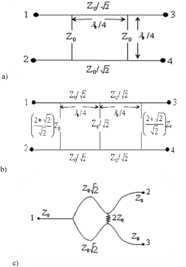
Some basic circuits are frequently used in microstrip technology for the realization of couplers [BAH 88, TUR 01]. The first is the 3 dB branch line coupler (90°, −3 dB), widely used in microwave applications (Figure 8.10a). This is characterized by two outputs of equal amplitude but phase shifted by 90°. To increase the bandwidth of the coupler, a second (or several) stage can be added as shown in Figure 8.10b. A bandwidth of around 25% can generally be obtained. However, the final dimensions are large compared to those of the single branch line coupler (bandwidth of about 10%).
180° phase shifters based on matched hybrid T or Rat-race hybrid can also be obtained on the same principle [BAH 88]. If equal-phase and equal-magnitude power dividing on one octave is desired, Wilkinson dividers are generally used (Figure 8.10c). Modification on the characteristic impedance of each branch allows unequal split of the signal if needed and multi-section structures enable isolation and bandwidth performances over more than one octave.
Figure 8.10. a) 3 dB branch line coupler; b) Double branch line coupler; c) Wilkinson coupler
8.6.2.3. Active microwave phase shifters
Several semiconductor diode phase shifters have been proposed in the literature. If solutions based on switching line sections of different lengths are not considered, most of them use a reflection phase shifter and operate on the phase difference created between an incident wave and a reflected wave from a reactance loaded line. The phase variation is then achieved by a continuous variable reactive element, such as a variable capacitance varactor diode and the separation of the incident wave and the reflected wave is obtained using for example a 3dB-90° branch line coupler [KLY 97, TUR 01].
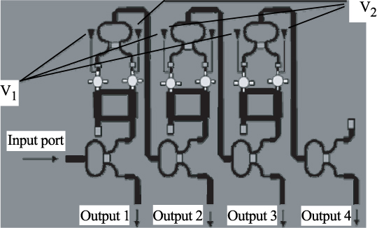
Another family of phase shifters is based on field effect transistors (FET). The proposed principle for a continuous phase shifter is to perform a vector addition of two signals having a phase shift of 90° and different magnitudes [KUM 81]. For this, the RF signal is first divided into two identical signals but with a phase difference of 90° (through a 3 dB branch line coupler for example). These signals are then applied to two identical amplifiers with variable gains but whose outputs are added (Wilkinson). By varying the gains of the two amplifiers independently, the result of this addition can take several values in amplitude, but in a more interesting way, phase shifts from 0 to 90° can also be obtained. To obtain only different phase shifts without changing of the magnitude, the quantity ![]() , where A and B are the magnitudes of the output signals of both FET amplifiers, has to be kept constant. The following circuit illustrates this principle. It uses two FETs in common source mode, and controlled by the drain voltage. This voltage varies between 0 and 5 volts. By combining several phase shifters, a phase law from 0 to 90°can be obtained, such as for example in Figure 8.11, where a feeding network of four elements is presented [TUR 01].
, where A and B are the magnitudes of the output signals of both FET amplifiers, has to be kept constant. The following circuit illustrates this principle. It uses two FETs in common source mode, and controlled by the drain voltage. This voltage varies between 0 and 5 volts. By combining several phase shifters, a phase law from 0 to 90°can be obtained, such as for example in Figure 8.11, where a feeding network of four elements is presented [TUR 01].
Figure 8.11. Four output phase shifter
Finally, based on the properties of hybrid circuits described in section 6.2.1, directly reconfigurable phase shifter circuits have emerged in recent years [FER 09a, FER 09b, FER 09c]. These circuits can be achieved using the hybrid microwave integrated circuit (MIC) technique. In this technology, all passive components are arranged on the surface of a low losses dielectric substrate and solid-state active devices are connected or welded to the passive circuits. In monolithic microwave integrated circuit (MMIC) technology, the entire circuit made up of passive and active elements, is performed on a semiconductor substrate. The main advantages of MMIC technology compared to the MIC are the small footprint and a low weight, which must also be added to an excellent reproducibility and the ability to include more functions on a single chip [BAH 88, MON 06].
8.6.3. Antennas with integrated phase shifters
Using appropriate values for phase and magnitude laws, electronic beam steering can be obtained. Another advantage presented by microstrip circuits is that it is possible, because of their technology and their dimensions depending on substrates, to think about their integration within the antenna using the technique of multilayer structures. This technique, used to create circular polarization in a hybrid coupler stacked on a radiating patch [TAR 95], yields radiation patterns quite similar to those obtained with a simple classical patch. However, in these types of structures, both phase shifter and patch must have their own ground plane.
[TUR 99b] presents an antenna integrating a phase shifter stacked on the patch. For the antenna, the ground plane remains unchanged. For the phase shifter, the ground plane is formed by the radiating element itself. This device is fed by connecting the outer conductor of the coaxial cable to the radiating patch, the central conductor of the cable being itself electrically connected to the input of the phase shifter. To minimize radiation perturbations, a technique involves passing the RF cable to the center of the patch, where the electric field is null for the fundamental mode. The phase shifter output is then connected to the ground plane of the patch to the point of desired impedance.
To illustrate the usefulness of this technology, an antenna application with an integrated power supply operating in the mobile PCS standard frequency band (1850–1990 MHz) is presented in more details here [TUR 99c]. It shows the feasibility of jointly incorporating a printed antenna, an amplifier and a phase shifter, which significantly reduces the problem of the size and complexity of power supply circuits.
Indeed, another advantage is to integrate all the functions in a single radiating element device, allowing easy production in large numbers for phased arrays. This type of phased array may be used in low power base stations. The antenna has an integrated amplifier and phase shifter enabling us to obtain a signal whose phase can be shifted from 0 up to100 degrees throughout the PCS frequency band and whose amplitude varies from 0 dB to 8 dB. The phase shift is achieved by using a branch line coupler (−3 dB, 90°) loaded by two varactor diodes whereas the signal amplification is achieved through a field effect transistor. The geometry of the proposed antenna is shown in Figure 8.12.
Figure 8.12. a)Integrated phase shifter-amplifier antenna; b) phase shifter-amplifier top view; c) measured S21 magnitude; d) measured S21 phase; e) measured S11 antenna return loss
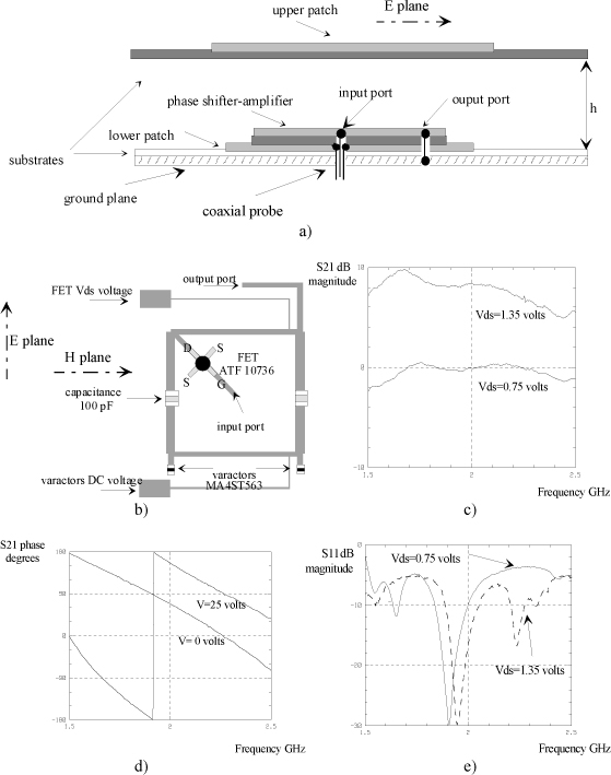
Stacked resonators have been widely applied to printed antennas to enlarge the bandwidth. In the proposed structure, only the lower element is fed by the output of the amplifier/phase shifter circuit. The second element, positioned above, is excited by electromagnetic coupling with the lower active element. This coupling can be adjusted to obtain a dual-band frequency or a broadband behavior depending respectively on if both resonances are sufficiently spaced or close. The field effect transistor operates in a grounded source mode and the gain of the transistor is then only controlled by means of the drain voltage Vds. To individually bias the varactors and the FET, two stubs are connected to the hybrid coupler and two DC bias wire connections are soldered onto them. HF capacitances of 100 pF are also used to separate the two DC voltages. The coaxial probe is not used to bring one of the two DC voltages because this structure is intended to be associated in phased arrays and each antenna has to be independently controlled. The phase of the signal can be controlled from 113 to 217°, i.e. a phase shift of 104° for a DC voltage from 0 to 25 V. The controlled amplification can be chosen from 0 to around 8 dB for the two extreme drain voltage values 0.75 and 1.35 V applied. Measurement of the return loss against frequency, also presented in Figure 8.12 for the two values of the DC drain FET voltage 0.75 and 1.35 V exhibits an S11 lower than −10 dB in the entire band. The radiation pattern, not presented here, is quite similar to that of simple passive microstrip antennas and this also makes it suitable for array applications.
8.7. Polarization agile antennas
Polarization agility can be employed to fight the possible depolarization of the electromagnetic field received, but also to realize polarization diversity operation. The solution initially used to modify the polarization of a printed antenna was generally based on switching different feed points for exciting different modes of the radiating element. This idea of switching feed points will still be used much later in the case of feeding slots. [YAN 02] proposes such a slot fed patch switchable using PIN diodes. However, in the early 1980s, Schaubert et al. [SCH 81] already showed a patch antenna solution with polarization agility achieved by switching four pairs of PIN diodes, allowing us to choose from three linear polarizations (horizontal, diagonal and vertical) and two circular polarizations (right and left). Linear polarizations are obtained by selecting different resonant modes in the patch and circular polarizations by means of lower perturbations of the cavity modes used to degenerate two orthogonal modes, a solution often employed to create circular polarization in a single access patch.
A solution based on the same principle, but using varactor diodes is presented later [HAS 94]. Another solution using the principle of capacitive loads on two different orthogonal edges of a square patch is presented in [HAS 95]. The load obtained by using bipolar transistors artificially modifies the electrical equivalent dimensions of the patch, and successfully changes the state of polarization. Many other solutions exist. Some of them use the modification of the excitation obtained by slot coupling using controllable couplers but also by MEMS for a mechanical modification of the shape of the antenna to obtain the desired polarization [LEG 04].
8.8. Self-adjusting antennas
As one of the radioelectric characteristic of an antenna becomes controllable, a negative feedback could be applied keeping the desired initial behavior of the antenna in terms of resonance frequency, polarization and radiation pattern. The most easily adjustable characteristic is probably the radiation pattern in the case of antenna arrays with controllable phase-shifters and amplifiers [GAN 63]. The received power level is simply permanently analyzed and when a decrease is observed, an electronic scanning searches to locate the new main direction of propagation.
8.8.1. Self adjusting frequency agile microstrip antennas
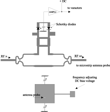
The principle of a frequency self adjusting microstrip antenna is not only a simple scan to find a transmitting channel as in reconfiguration but also consists of being able to keep the resonant frequency chosen for the antenna, despite a fast modification of its close environment (temperature fluctuations, dielectric or conductive objects in its immediate vicinity, etc.). Printed antennas, with important quality factors and very narrow frequency bandwidths are particularly sensitive to external disturbances which are inclined to change the resonance behaviour of the antenna in a random way, which becomes less efficient for transmitting the signal at the dedicated frequency. An extra emitting power is usually used to maintain a sufficient link budget despite a possible mismatch of the antenna. However in 1992, a study to improve antenna performances was already done by White and Van Der Valt using a miniature self-adjusting loop antenna used in VHF and UHF bands [WHI 92]. The structure presented in [TUR 99a] also solves this detuning problem (Figure 8.13). The initial microstrip antenna, loaded by two varactor diodes, is well matched at the desired resonance frequency when there is no environment perturbation for a correct reverse DC voltage applied on the diodes. Self-adjusting is obtained by comparing the incoming signal on the printed antenna and the possible reflected signal in the case of perturbation, in order to realize an automatic feedback on the antenna. This is possible using the well-known frequency effects of varactor diodes inserted on the radiating edges of the antenna.
The difficulty of tuning an antenna is then not to modify the frequency but to know if the loss of transmitted power due to a reflected signal is created because of the increase or the decrease of the resonance frequency. In the case of a microstrip patch — the input impedance locus described by a circle on the Smith chart with the desired resonance frequency initially matched — when the antenna is tuned out, the impedance locus turns and then an imaginary part appears. This imaginary part depends on the way the resonance frequency has changed. If it has increased, the impedance becomes inductive, otherwise it will be capacitive. Then, the incident and reflected signals being out of phase, a phase comparison between the two signals allows us to determine the new resonance frequency. If the frequency has increased, the incident signal will have a positive phase difference, otherwise, this phase difference will be negative. By applying these two signals to the inputs of a phase comparator, we obtain a DC output signal proportional to the sign of the phase difference. If the resonance frequency of the patch increases versus the voltage applied to the varactor diodes, then the voltage needed to correct a frequency shift must decrease. To obtain this characteristic, the DC voltage delivered by the phase comparator is amplified and added to the permanent voltage corresponding to the desired resonance frequency when there is no disturbance. Then, this negative feedback enables correction of a non-desired frequency shift. Nowadays, other systems based on the tuning of additional matching circuits inserted between the antenna and the RF lines exist and comparison between the two techniques in terms of advantages and drawbacks should be made.
Figure 8.13. Self-adjusting frequency microstrip antenna circuit design
8.8.2. Self-adjusting polarization agile microstrip antennas
In the case of a depolarization of the electrical field, a linearly polarized antenna becomes less efficient, which results in a more or less important decrease in the amplitude of the received signal. A self-adjusting polarization agile antenna can be a solution to overcome this drawback [TUR 00]. To obtain this negative feedback, the system must contain two parts. The first part is an adjusting polarization agile antenna enabling modification of the electrical field polarization direction. The second part must allow determination of the new polarization direction of the electric field received by the antenna after depolarization.
The possible solution presented in Figure 8.14 is described in [TUR 00]. This antenna is made up of a square microstrip patch, coaxially fed on its diagonal and having two orthogonal radiating edges loaded in their middle by two independently biased varactor diodes. Two coupled microstrip lines are printed close to the two other edges of the patch. To convert the received RF signal into a DC signal, Schottky diodes and capacitances are used, and the matching of these circuits is done by adding a resistor at the end of each line.
Figure 8.14. Self-adjusting polarization microstrip antenna circuit design
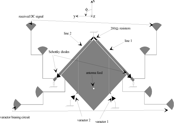
The operating principle is to use the polarization of the received electrical field to control the varactor biasing and then the antenna polarization. This is made possible by the association of the two coupled microstrip lines on the edges of the patch. When the received signal is vertically polarized, the two lines receive the same level of signal. Otherwise, one of these lines will retrieve a higher level than the other (by direct reception more than by coupling) and the information of depolarization is then obtained. By converting the obtained signals into two DC voltages proportional to the magnitude of each RF signal and using two comparators, the difference between these two signals will allow us to determine the direction of the incident wave polarization.
The change of antenna polarization is made possible by using these same DC signals to independently bias the two varactor diodes and then to obtain an electrically equivalent modification of the geometry of the patch. DC voltages are applied through two microstrip isolation stages used to inject the DC current without perturbation of the HF (section 8.6.2.1). To correctly separate the DC signals on each varactor, thin slots on the patch have been made, as far as possible from the probe. To ensure good RF current continuity and an efficient effect of the diodes, the patch is covered first by an insulating layer then by a conducting layer.
8.9. Conclusion
This chapter has attempted to give the state of the art and some potential solutions in the domain of frequency, radiation pattern and polarization reconfiguration of different types of printed or planar radiating elements. The main feeding techniques and active components used have been described to enable a better understanding of the techniques presented. Many other solutions on the different points developed may be obtained from the proposed references and those in the bibliography.
8.10. Acknowledgements
I wish to thank everyone who contributed to this theme developed in the LEAT for several years and whose work is cited here.
8.11. Bibliography
[ABE 92] ABERLE J.T., CHU M., BIRTCHER C.R., “Scattering and radiation properties of varactor-tuned microstrip antennas”, IEEE Antennas and Propagation Society International Symposium AP-S, pp. 2229–2232, 1992.
[BAH 88] BAHL I., BHARTIA P., Microwave Solid State Circuit Design, John Wiley & Sons, New York, 1988.
[BHA 82] BHARTIA P., BAHL I.J., “Frequency agile microstrip antennas”, Microwave Journal, vol. 25, pp. 67–70, October 1982.
[BIL 02] BILLARD C., CHARVET P.L., FORT C., “RF MEMS thermally actuated switch for communication systems”, European Workshop on Integrated Radio Communication Systems, IEEE AP-S and MTT-S French, Angers, May 2002.
[CAR 01] CARRERE J.M., Antennes multinormes pour systèmes de télécommunications mobiles, PhD thesis, University of Nice-Sophia Antipolis, September 2001.
[CHA 02] CHANG K., YORK R. A., HALL P.S., ITOH T., “Active Integrated Antennas”, IEEE Transactions on Microwave Theory and Techniques, vol. 50, no. 3, pp. 937–943, March 2002.
[CHE 03] CHEN Q., KURAHASHI M., SAWAYA K., “Dual-mode patch antenna with PIN diode switch”, Antennas, Propagation and EM Theory 6th International Symp., pp. 66–69, 2003.
[DUB 85] DUBOST G., RABBAA A., “Substrate influence on flat folded dipole bandwidth”, Electronics Letters, vol. 21, no. 10, pp. 426–427, May 1985.
[FEL 07] FELDNER L. M., RODENBECK C. T., CHRISTODOULOU C. G., KINZIE N., “Electrically small frequency-agile PIFA-as-a-package for portable wireless devices”, IEEE Transaction on Antennas and Propagation, Vol. 55, no. 11, pp. 3310–3319, November 2007.
[FER 07a] FERRERO F., LUXEY C., STARAJ R., JACQUEMOD G., FUSCO V., “Compact quasilumped hybrid coupler tunable over a large frequency band”, Electronics Letters, vol. 43, no. 19, p. 1030–1031, September 2007.
[FER 07b] FERRERO F., Reconfiguration dynamique d’antennes imprimées en directivité et polarisation, PhD Thesis, University of Nice-Sophia Antipolis, November 2007.
[FER 09a] FERRERO F., LUXEY C., STARAJ R., JACQUEMOD G., YEDLIN M., FUSCO V., “Patch antenna with linear polarisation tilt control”, IET Electronics Letters, vol. 45, no. 17, pp. 870–872, 13 August 2009.
[FER 09b] FERRERO F., LUXEY C., STARAJ R., JACQUEMOD G., YEDLIN M., FUSCO V., “A novel quad-polarization agile patch antenna”, IEEE Transactions on Antennas and Propagation, vol. 57, no. 5, pp. 1562–1566, May 2009.
[FER 09c] FERRERO F., LUXEY C., STARAJ R., JACQUEMOD G., YEDLIN M., FUSCO V., “Theory and design of a tunable quasi-lumped quadrature coupler”, Microwave and Optical Technology Letters, vol. 51, no. 9, pp. 2219–2222, September 2009.
[FUJ 87] FUJIMOTO K., HENDERSON A., HIRASAWA K., JAMES J.R., Small Antennas, Research Studies Press, John Wiley & Sons, New York, 1987.
[GAN 63] GANGI A., “The active adaptative antenna array system”, IEEE Transactions on Antennas and Propagation, vol. 11, no. 4, pp.405–414, 1963.
[HAS 94] HASKINS P.M., DAHELE J.S., “Varactor-diode loaded passive polarisation-agile patch antenna”, Electronic Letters, vol. 30, no. 13, pp. 1074–1075, June 1994.
[HAS 95] HASKINS P.M., DAHELE J.S., “Compact active polarisation-agile antenna using square patch”, Electronic Letters, vol. 31, no. 16, pp. 1305–1306, August 1995.
[ITO 97] ITOH T., “Active integrated antenna for wireless applications”, Asia Pacific Conference, 3A 01-4 pp.309–312, 1997.
[JAM 89] JAMES J.R., HALL P.S., Handbook of Microstrip Antennas, Peter Peregrinus Ltd, London, 1989.
[KAN 08] KANAUJIA B. K., SINGH A. K., VISHVAKARMA B. R., “Impatt diode integrated annular ring microstrip antenna”, Microwave and Optical Technology Letters, vol. 50, no. 6, June 2008
[KAR 02] KARMAKAR N.C., BIALKOWSKI M.E., “High performance L-band series and parallel switches using low-cost PIN diodes”, Microwave and Optical Technology Letters, vol. 32, no. 5, 5 March 2002.
[KIV 02] KIVEKAS O., OLLIKAINEN J., VAINIKAINEN P., “Frequency tunable-internal antenna for mobile phones”, Journées Internationales sur les Antennes JINA 2002, vol. 2, pp. 53–56, Nice, November 2002.
[KLY 97] KLYMYSHYN D. M., KUMAR S., MOHAMMADI A., “Linear reflection phase shifter with optimized varactor gamma”, IET Electronics Letters, vol. 33, no. 12, pp.1054–1055, 5 June 1997.
[KOL 98] KOLSRUD A.T., LI M.Y., CHANG K., “Dual frequency electronically tunable CPW fed CPS dipole antenna”, Electronic Letters, vol. 34, no. 7, pp. 609–611, 2 April 1998.
[KUM 81] KUMAR M., MENNA R.J., HUANG H.-C., “Broadband active phase shifter using dual — gate MESFET”, IEEE Microwave Theory and Techniques, vol. 29, pp. 1098–1101, October 1981.
[KWO 79] KWOK S.P., WELLER K.P., “Low cost X-band MIC BARITT Doppler Sensor”, IEEE Transactions on Microwave Theory and Techniques, vol. 27, no. 10, pp. 844–847, October 1979.
[LAH 01] LAHEURTE J.M., “A switchable CPW-fed slot antenna for multifrequency operation”, Electronic Letters, vol. 37, pp. 1498–1500, 6 December 2001.
[LEG 04] LE GARREC L., Etude et conception en bande millimétrique d’antennes reconfigurables basées sur la technologie des MEMS, PhD Thesis, University of Rennes, November 2004.
[LU 98] LU J.-H., TANG C.-H., WONG K.-L., “Slot-coupled compact broadband circular microstrip antenna with chip-resistor and chip-capacitor loading”, Microwave and Optical Technology Letters, vol. 18, no. 5, 5 August 1998.
[LUX 00] LUXEY C., DUSSOPT L., LE SONN J.-L., LAHEURTE J.-M., “Dual-frequency operation of a CPW-fed antenna controlled by PIN diodes”, Electronic Letters, vol. 36, no. 1, pp. 2–3, 6 January 2000.
[LUX 07a] LUXEY C., STARAJ R., KOSSIAVAS G., PAPIERNIK A., Antennes imprimées. Bases et principe, Fasc. E3310, Techniques de l’Ingénieur, Série Electronique, 2007.
[LUX 07b] LUXEY C., STARAJ R., KOSSIAVAS G., PAPIERNIK A., Antennes imprimées. Techniques et domaines d’applications, Fasc. E3311, Techniques de l’Ingénieur, Série Electronique, 2007.
[MON 06] MONTUSCLAT S., GIANASELLO F., GLORIA D., “Silicon full integrated LNA, filter and antenna system beyond 40 GHz for MMW wireless communication links in advanced CMOS technologies”, RFIC Symposium, 2006.
[NAV 96] NAVARRO J.A., CHANG K., Integrated Active Antennas and Spatial Power Combining, John Wiley & Sons, New York, 1996.
[PAN 01] PANAYI P.K., AL-NUAIMI M.O., IVRISSIMTZIS L.P., “Tuning techniques for planar inverted-F antenna”, Electronic Letters, vol. 37, no. 16, pp. 1003–1004, 2 August 2001.
[PAN 06a] PANAÏA P., LUXEY C., JACQUEMOD G., STARAJ R., PETIT L., DUSSOPT L., “Multistandard reconfigurable Pifa antenna”, Microwave and Optical Technology Letters, vol. 48, no. 10, pp. 1975–1977, October 2006.
[PAN 06b] PANAÏA P., Reconfiguration dynamique d’une antenne pour partages de fonctions, PhD Thesis, University of Nice-Sophia Antipolis, December 2006.
[PER 86] PERKINS III T.O., “Microstrip patch antenna with embedded Impatt oscillator”, IEEE Antennas and Propagation Society International Symposium AP-S, pp. 447–450, 1986.
[PER 87] PERKINS III T.O., “Active microstrip circular patch antenna”, Microwave Journal, vol. 30, no. 3, pp. 109–117, March 1987.
[PET 79] PETERSEN K.E., “Micromechanical membrane switches on silicon”, IBM Journal on Research Development, vol. 23, no. 4, pp. 376–385, July 1979.
[PET 06] PETIT L., DUSSOPT L., LAHEURTE J.-M., “MEMS-switched parasitic-antenna array for radiation pattern diversity”, IEEE Transaction on Antennas and Propagation, vol. 54, no. 9, pp. 2624–2631, September 2006.
[REB 01] REBEIZ G.M., MULDAVIN J.B., “RF MEMS switches and switch circuits”, IEEE Microwave Magazine, vol. 2, no. 4, pp. 59–71, December 2001.
[REB 03] REBEIZ G.M., RF MEMS Theory, Design and Technology, John Wiley & Sons, New York, 2003.
[RIC 01] RICHARDS R.J., DE LOS SANTOS H.J., “MEMS for RF/Wireless Applications: The Next Wave”, Microwave Journal, March 2001.
[SAI 03] SAIAS D., ROBERT P., BORET S., BILLARD C., BOUCHE G., BELOT D., ANCEY P., “An above IC MEMS RF switch”, IEEE Journal of Solid-State Circuits, vol. 38, no. 12, pp. 2318–2324, December 2003.
[SCH 80] SCHAUBERT D., FARRAR F., SINDORIS A., HAYES S., “Frequency agile microstrip antennas”, IEEE Antennas and Propagation Society International Symposium AP-S, vol. 18, no. 1, pp. 601–604, 1980.
[SCH 81] SCHAUBERT D., FARRAR F., SINDORIS A., HAYES S., “Microstrip antennas with frequency agility and polarization diversity”, IEEE Transaction on Antennas and Propagation, vol. 29, no. 1, pp. 118–123, January 1981.
[SCH 04] SCHLUB R.W., Practical realization of switched and adaptative parasitic monopole radiating structures, PhD report, Griffith University, January 2004.
[SHY 05] SHYNU S.V., AUGUSTIN G., KANANSAN C., MOHONAN P., VASUDEVAN K., “A reconfigurable dual-frequency slot-loaded microstrip antenna controlled by PIN diodes”, Microwave and Optical Technology Letters, vol. 44, no. 4, 20 February 2005.
[TAR 95] TAROT A.-C., Etude d’antennes à faible coût pour les télécommunications avec les mobiles, PhD Thesis, University of Rennes, 20 December 1995.
[TUR 99a] TURKI Y., STARAJ R., “Self adjusting microstrip antenna”, Electronic Letters, pp. 106–107, January 1999.
[TUR 99b] TURKI Y., STARAJ R., “Microstrip antenna with integrated phase shifter”, Microwave and Optical Technology Letters, vol. 22, no. 6, pp. 393–394, September 1999.
[TUR 99c] TURKI Y., STARAJ R., “Microstrip antenna with integrated amplifier and phase shifter for DCS applications”, Electronic Letters, vol. 35, no. 23, pp. 1983–1985, November 1999.
[TUR 00] TURKI Y., STARAJ R., “Polarisation agile self-adjusting microstrip antenna”, Microwave and Optical Technology Letters, 20 August 2000.
[TUR 01] TURKI Y., Dispositifs actifs d’alimentation de réseaux d’antennes conformes, PhD Thesis, University of Nice-Sophia Antipolis, July 2001.
[WAT 07] WATERHOUSE R.B., SHULEY N.V., “Frequency agile microstrip rectangular patches using varactor diodes”, IEEE Antennas and Propagation Society International Symposium AP-S, pp. 2188–2191, 1992.
[WHI 92] WHITE F., VAN DER VALT P.W., “Miniature self-adjusting loop antenna”, Electronics Letters, vol. 24, pp. 2075–2076, 1992.
[YAN 02] YANG F., RAHMAT-SAMII Y., “A reconfigurable patch antenna using switchable slots for circular polarization diversity”, IEEE Microwave and Wireless Comp. Letters, vol. 12, no. 3, pp. 96–98, March 2002.
1 Chapter written by Robert STARAJ.