
Chapter 10
High Impedance Surface Close to
a Radiating Dipole1
10.1. Introduction
High impedance surfaces seem to be very attractive for design engineers who at first glance see the opportunity to reduce the thickness of all kinds of antennas using dipoles. The reason is that at the frequency at which the impedance of the surface reaches a high value, it is possible to get a good dipole radiation with an input impedance of the dipole close to 50 Ohms.
In order to check this attractive property, we have studied, fabricated and measured a circuit made of a dipole placed very close to a high impedance surface (HIS). This HIS contains resonant line patterns called 2LC which have been studied by L.Y. Zhou, H. Ouslimani from GEA Université Paris Ouest Ville d’Avray France. We will present in the following sections, firstly the description of the circuits, secondly the main results obtained and after that we will discuss the difficulties encountered and propose some physical explanations for the phenomena.
10.2. Antenna study
The antenna which has been defined is made of a dipole fed by a balun and placed above a dielectric substrate. On one side of the substrate there is a ground plane and on the other side, the microstrip lines that make up the resonant circuits called 2LC. The dipole has been initially designed in order to have a length close to half a wavelength at the central frequency. Later, after the introduction of the HIS below the dipole, it was necessary to reduce the length of the dipole arms in order to compensate for the coupling effects. The HIS itself has been studied following a classical approach that consists of looking for the resonant frequency of the 2LC circuit with a TEM wave impinging normally to the circuit.
Figure 10.1. Complete structure with dipole, metallic grid composed of elementary cells and balun
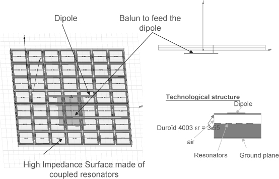
The 2LC circuit is a closed square loop with a perimeter length equal to one wavelength at the resonant frequency. Some complementary lines are added to this basic shape. They are very high impedance lines connected to opposite sides of the square and almost joined in the centre, in order to produce a capacitor by proximity effect (see Figure 10.1).
Due to this specific design, the 2LC pattern works as a double resonator with one mode corresponding to the resonance of the peripheral loop characterized by a voltage node at the connection point with the transverse lines which is of no influence on this first resonance. The second mode corresponds to a 90° rotation of the fields patterns so that in that case, the transverse lines have a capacitive effect.
When the resonant frequency of the two modes are tuned to be identical, we can obtain a relatively large frequency bandwidth of about 6% around 1.1 GHz.
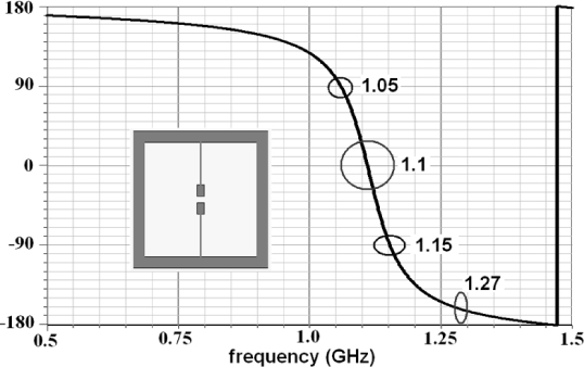
When a TEM wave is impinging on the HIS, we observe the reflection coefficient of the wave that rapidly varies around a resonance frequency: the amplitude has a spike and its phases range from +180° to −180°. The practical usable bandwidth is defined between +90° and −90°. The high impedance condition is really met at the frequency at which the phase is 0° (see Figure 10.2).
Figure 10.2. Phase variation of the reflection coefficient at a frequency close to the resonance
When the elementary circuit pattern is tuned, the next design step consists of placing the 2LC cells at a regular distance in x and y in order to build an array. The distance between the neighbors directly influences the electrical and magnetic couplings between the cells. The whole assembly looks like a metallic grid. The distance between the dipole and the grid is a tuning parameter as well as the length of the dipole. The arms of the dipole are shortened in order to tune the dipole resonance to be identical to the grid resonance.
The measurement of the reflection coefficient at the dipole input shows a quite narrow matched bandwidth which looks like the resonance of the HIS. A graph presenting this figure is plotted in Figure 10.3.
Figure 10.3. Reflection coefficient at the input of the dipole placed above the high impedance surface
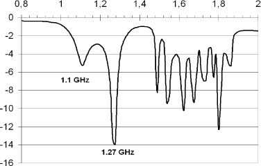
In contradiction with the simulation, the measurement shows that there are two frequency areas where the matching is favorable, the first one around 1.1 GHz and the second one around 1.27 GHz. The question is now to identify which of those two frequency areas corresponds to the high impedance behavior of the surface.
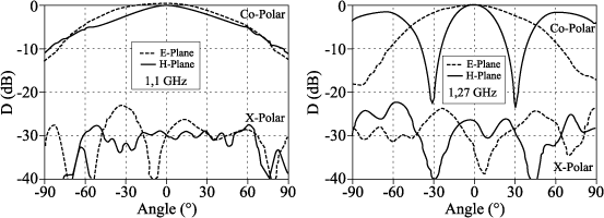
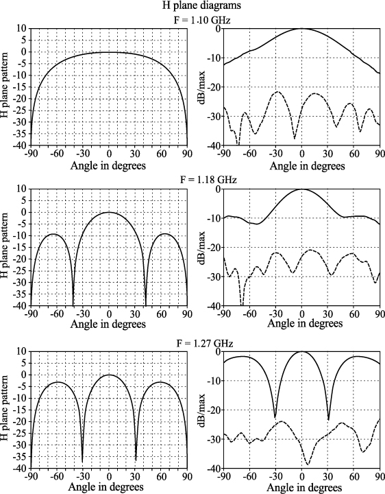
The radiating patterns measured on the prototypes also show an unpredicted behavior. As can be seen in Figure 10.4, the patterns in the E plane, parallel to the dipole and in the H plane, perpendicular the dipole do not experience the same evolution inside the frequency band. At 1.1 GHz which is the frequency of the first resonance spike of the reflection coefficient, the patterns in the E and H plane have canonical shapes, similar to cosine functions. On the contrary, at the frequency of the second spike (1.27 GHz), the E plane pattern remains normal while the H plane pattern is seriously transformed into three lobes.
Figure 10.4. Radiating patterns in the E and H planes
10.3. Analysis of the phenomena
In order to try to understand the phenomena involved, it is necessary first to more precisely characterize the electrical nature of the HIS. In fact, as the HIS is working as a distributed resonator, and like every resonant circuit, it can be explained with an analogy to R-L-C resonators, in either series or shunt configuration. The wave that arrives on the dielectric substrate experiences two successive reflections: one due to the ground plane and the other due to the resonant cells located on the surface. The ground plane short circuit impedance seen in the interface plane between air and circuit acts as a small inductance in parallel with the LC resonator of the cells. The combined impedance of these two effects is given by the following expression:
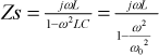
The plot of the imaginary part of the total surface impedance is shown in Figure 10.5. We can easily identify a resonance at the central frequency. At frequencies below the resonance, the imaginary part of the impedance is positive which means that the surface impedance is inductive while above the resonance, the imaginary part of the impedance is negative which means that the impedance is capacitive. This first element is precious because it will help us to understand under which condition the different propagation modes can propagate in this open and inhomogeneous structure, made of a dielectric grounded substrate on one side and air on the other side.
This kind of structure makes the propagation of plane waves possible. These are called inhomogeneous waves and can either be slow waves and propagate on the surface of the substrate (surface waves) or be fast waves and radiate (leaky waves).
Using the axis parallel to the substrate as the reference axis for the propagation, we can classify the propagating waves in TE modes (the 2 components of the electric field are in the plane perpendicular to propagation axis) and in TM modes (the 2 components of the magnetic field are in the plane perpendicular to the propagation axis).
The table in Figure 10.6 indicates the main characteristics of the TE and TM modes propagating in the vicinity of the surface. These modes are either surface waves which do not radiate, or leaky waves which radiate.
Figure 10.5. Variation of the imaginary part of the surface impedance
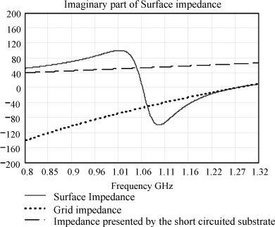
Figure 10.6. Classification of the modes related to the nature of the surface
The classification of the present modes into TE and TM modes is however insufficient. Indeed, it assumes a wave propagation in a uniform medium made of air on one side and a dielectric substrate on the other. It does not take into account the presence of microstrip lines that make up the grid where the TEM mode can propagate.
By the way, the global structure can support TE and TM waves propagating on the surface or directly radiating in the air, and TEM guided modes propagating inside the grid lines.
The analysis of these propagation mechanisms must take all these factors into consideration.
In order to compare this description of the possible modes to some measurements, the antenna prototype has been modified: microstrip lines have been added on the substrate on each side of the dipole. Thanks to these lines, it has been possible to evaluate the way a TEM wave injected on one of the lines has been able to reach the opposite side of the dipole after having propagated inside the structure.
The transfer function between the input of the first line and the output of the second line is the direct expression of the propagation of waves inside the grid through the different possible modes. Furthermore, the grid can easily be described by a circuit simulation considering only the TEM mode, which will only give partial information, but which is however interesting when compared to the measurement.
This comparison is indicated in Figure 10.7. On the measured curve we can easily see that at low frequency, the attenuation is very high and there is a cut-off frequency above which a bandpass area appears. On the left side of this filter skirt, we can identify a first discontinuity indicated by the marker 1 at 1.1 GHz, and then a second spike of the transfer function at 1.27 GHz. On the transfer function curve of the simulated grid for the TEM mode, we can see the left side of the filter skirt is much steeper with only one spike at the beginning of the bandpass area at 1.27 GHz.
The lessons learned from these graphs can be summarized in the table displayed in Figure 10.8. When the dipole is fed, it radiates and creates modes in the whole structure as well as the microstrip lines of the grid. Firstly modes TE and TM are excited. Below the resonant frequency of the surface (called ω0 in the table) that can be associated with the frequency 1.1 GHz, the surface is inductive and can only support a TE leaky wave mode and a TM surface mode. Moreover, as we have seen no default on the radiation pattern of the structure below 1.1 GHz, we can reasonably conclude that from these 2 modes, only the TM mode exists and propagates inside the substrate. We also know that below 1.1 GHz, the TEM mode is strongly attenuated as suggested by the circuit analysis. This confirms the idea that below 1.1 GHz, only a surface mode in the substrate can propagate without effect on the radiation.
Figure 10.7. Transfer function of the grid: measurement on the left and simulation on the right
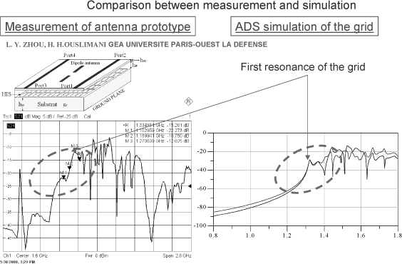
Figure 10.8. Mode generation inside the structure
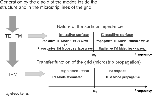
Above 1.1 GHz, the surface impedance has become capacitive and the structure can accept both a TE propagative mode and a TM leaky wave mode. The situation is even more complex because we observe that the TEM mode can also propagate inside the grid. At the same time we get three modes in this structure with radiation carried by the TM mode. By the way, we can observe that the radiated patterns are modified a lot in the H plane.
It is however justified to wonder whether the grid which has a symmetrical definition only propagates waves in the direction perpendicular to the dipole and not parallel to it. The explanation proposed is that along the dipole arms the phase of the current is constant and through couplings, the constant phase is maintained on the axis below each of the arms. On the contrary, the dipole arms will not make any opposition to phase variation along the perpendicular axis and that authorizes a wave propagation in this direction.
Figure 10.9. Structure modeled by Yakolev and result of the analytical study
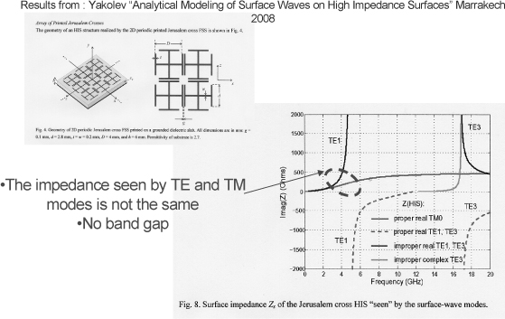
A detailed analytical study of a similar structure has been presented by Yarolev in a recent paper [YAK 08]. The structure analyzed was made of Jerusalem cross cells placed on a dielectric shorted by a ground plane. An analytical expression of the modes that can exist in this structure has led to the dispersion diagrams presented in Figure 10.9. It is of high interest to notice that there are modes of different kinds that can exist at the same time even in the low frequency region. We can see that the TM0 and TE1 have no cut-off frequency and that they are present at very low frequency. The TM0 mode is called “proper real” which means that it is a surface propagative mode in the whole frequency band while the TE1 mode is called “improper real” which means that it is a leaky wave below a frequency close to 5 GHz and then becomes “proper real” above this resonance frequency. It is clearly noticeable that the analyzed structure does not present any high impedance area which would be a necessary condition for placing a dipole very close to the surface. Based on this example developed with the precise information given by the analytical model, we become conscious of how difficult it is to realize favorable conditions for the dipole to radiate close to a ground place, taking advantage of a true HIS with a band gap for all possible modes.
10.4. Phenomenological model of the radiating array
The study of the propagation on the TEM mode inside the grid helps us to know the amplitude and phase values of the signals which feed the different cells of the grid. These cells can be assimilated to the radiating elements of an array. In particular, we can notice that due to the resonant property of the cells, the phase experiences a 180° variation from one cell to another on the axis perpendicular to the dipole. Therefore, the grid makes up an array for which central elements are directly coupled to the dipole and the off-centered elements are fed by a propagative wave inducing a phase shift of 180° from one cell to another. While propagating inside the grid, the wave is attenuated and excites the elements of the edges with a weighted amplitude.
The radiating pattern is strongly affected by the phase inversion between one radiating element and its direct neighbors. In the array factor calculation, we have introduced amplitude and phase coefficients conformal to the physical behavior previously described. By adjusting the amplitude of the coefficients on elements located close to the edge, it is easy to simulate a shape of the radiating patterns identical to those measured at frequencies higher than 1.27 GHz (see Figure 10.10).
This verification clearly confirms the mechanisms of the wave propagation inside the grid and the way the different cells of the grid take part in the radiation of the structure. Therefore, above the resonance frequency of 1.27 GHz, we no longer have a dipole that takes profit from the structured high impedance surface. We do have a mixed structure with a dipole and a radiating grid for which elementary cells behave like radiating elements of an array fed by the wave propagation inside the grid. At that moment, it becomes difficult to distinguish between the surface mode that feeds the radiating cells, the radiation of the cells, and the leaky wave that radiates naturally from the open structure with grounded dielectric on one side and open air on the other.
Figure 10.10. Comparison between simulation model and measurement for the radiating array
10.5. Conclusion
The high interest sparked by metamaterials inside the electromagnetic and antenna community is justified by the numerous properties that these new structures can provide. However, being confronted today with first circuit realizations, we discover that mastering these new circuits needs a precise knowledge of the complex propagation mechanisms inside these structures. For instance, the high impedance condition presented by a metamaterial surface is not fully realized as soon as there are different modes that can exist at the same time, presenting various impedances. The true condition will be verified only if the working frequency band really corresponds to a band gap for all possible modes.
There is still a significant analysis and simulation effort to be undertaken before being able to master the different possible modes and their cut-off frequency, in order to really benefit from the interesting properties that metamaterials could provide.
10.6. Bibliography
[YAK 08] A. B. YAKOVLEV, C. R. SIMOVSKI, S. A. TRETYAKOV, O. LUUKKONEN, G. W. HANSON, “Analytical modeling of surface waves on high impedance surfaces”, NATO ARW & META’08, Marrakesh, Morocco, 7–10 May 2008.
1 Chapter written by Olivier MAAS, Habiba OUSLIMANI and Luyang ZHOU.