
Chapter 3. Data Acquisition Hardware and Software
Although this chapter is primarily about analog-to-digital converters (ADCs), an understanding of digital-to-analog converters (DACs) is important to understanding how ADCs work. Figure 3.1 shows a simple resistor ladder with three switches. The resistors are arranged in an R/2R configuration. The actual values of the resistors are unimportant; R could be 10,000 or 100,000 or almost any other value. Each switch, S0–S2, can switch one end of one 2R resistor between ground and the reference input voltage, VR. The figure shows what happens when switch S2 is on (connected to VR) and S1 and S2 are OFF (connected to ground). By calculating the resulting series/parallel resistor network, the final output voltage (VO) turns out to be 0.5 × VR. If we similarly calculate VO for all the other switch combinations, we get the results listed in Table 3.1.
Figure 3.1. 3-bit DAC.
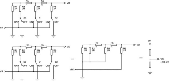
Table 3.1. VO for other switch combinations
| S2 | S1 | S0 | Vo |
|---|---|---|---|
| OFF | OFF | OFF | 0 |
| OFF | OFF | ON | 0.125 × VR (1/8 × VR) |
| OFF | ON | OFF | 0.25 × VR (2/8 × VR) |
| OFF | ON | ON | 0.375 × VR (3/8 × VR) |
| ON | OFF | OFF | 0.5 × VR (4/8 × VR) |
| ON | OFF | ON | 0.625 × VR (5/8 × VR) |
| ON | ON | OFF | 0.75 × VR (6/8 × VR) |
| ON | ON | ON | 0.875 × VR (7/8 × VR) |
If the three switches are treated as a 3-bit digital word, then we can rewrite Table 3.1 as Table 3.2 (using ON = 1, OFF = 0).
Table 3.2. Results of Table 3.1 with switches treated as a 3-bit digital word
| S2 | S1 | S0 | Equivalent logic state | S0–S2 numeric equivalent | ||
|---|---|---|---|---|---|---|
| S2 | S1 | S0 | ||||
| OFF | OFF | OFF | 0 | 0 | 0 | 0 |
| OFF | OFF | ON | 0 | 0 | 1 | 1 |
| OFF | ON | OFF | 0 | 1 | 0 | 2 |
| OFF | ON | ON | 0 | 1 | 1 | 3 |
| ON | OFF | OFF | 1 | 0 | 0 | 4 |
| ON | OFF | ON | 1 | 0 | 1 | 5 |
| ON | ON | OFF | 1 | 1 | 0 | 6 |
| ON | ON | ON | 1 | 1 | 1 | 7 |
The output voltage is a representation of the switch value. Each additional table entry adds VR/8 to the total voltage. Or, put another way, the output voltage is equal to the binary, numeric value of S0–S2, times VR/8. This three-switch DAC has eight possible states and each voltage step is VR/8.
We could add another R/2R pair and another switch to the circuit, making a four-switch circuit with 16 steps of VR/16 volts each. An eight-switch circuit would have 256 steps of VR/256 volts each. Finally, we can replace the mechanical switches in the schematic with electronic switches to make a true DAC.
3.1. ADCs
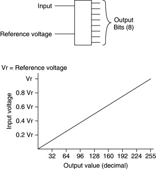
The usual method of bringing analog inputs into a microprocessor is to use an ADC. An ADC accepts an analog input, a voltage or a current, and converts it to a digital word that can be read by a microprocessor. Figure 3.2 shows a simple ADC. This hypothetical part has two inputs: a reference and the signal to be measured. It has one output, an 8-bit digital word that represents, in digital form, the input value. For the moment, ignore the problem of getting this digital word into the microprocessor.
Figure 3.2. Simple ADC.
3.1.1. Reference Voltage
The reference voltage is the maximum value that the ADC can convert. Our example 8-bit ADC can convert values from 0V to the reference voltage. This voltage range is divided into 256 values, or steps. The size of the step is given by
![]()
This is the step size of the converter. It also defines the converter's resolution.
3.1.2. Output Word
Our 8-bit converter represents the analog input as a digital word. The most significant bit of this word indicates whether the input voltage is greater than half the reference (2.5V, with a 5-V reference). Each succeeding bit represents half of the previous bit, as in Table 3.3, so a digital word of 0010 1100 is as represented in Table 3.4.
Table 3.3. Representation by each succeeding bit
| Bit: | Bit 7 | Bit 6 | Bit 5 | Bit 4 | Bit 3 | Bit 2 | Bit 1 | Bit 0 |
| Volts: | 2.5 | 1.25 | 0.625 | 0.3125 | 0.156 | 0.078 | 0.039 | 0.0195 |
Table 3.4. Representation of the digital word
| Bit: | Bit 7 | Bit 6 | Bit 5 | Bit 4 | Bit 3 | Bit 2 | Bit 1 | Bit 0 |
| Volts: | 2.5 | 1.25 | 0.625 | 0.3125 | 0.156 | 0.078 | 0.039 | 0.0195 |
| Output value: | 0 | 0 | 1 | 0 | 1 | 1 | 0 | 0 |
Adding the voltages corresponding to each bit, we get
![]()
3.1.3. Resolution
The resolution of an ADC is determined by the reference input and the word width. The resolution defines the smallest voltage change that can be measured by the ADC. As mentioned earlier, the resolution is the same as the smallest step size and can be calculated by dividing the reference voltage range by the number of possible conversion values.
For the example we have been using so far, an 8-bit ADC with a 5-V reference, the resolution is 0.0195V (19.5 mV). This means that any input voltage below 19.5 mV will result in an output of 0. Input voltages between 19.5 and 39 mV will result in an output of 1. Between 39 and 58.6 mV, the output will be 2. Resolution can be improved by reducing the reference input. Changing from 5V to 2.5V gives a resolution of 2.5/256, or 9.7 mV. However, the maximum voltage that can be measured is now 2.5V instead of 5V.
The only way to increase resolution without changing the reference is to use an ADC with more bits. A 10-bit ADC using a 5-V reference has 210, or 1024 possible output codes. So the resolution is 5V/1024, or 4.88 mV.
3.2. Types of ADCs
ADCs come in various speeds, use different interfaces, and provide differing degrees of accuracy. Three types of ADCs are illustrated in Figure 3.3.
Figure 3.3. ADC types.
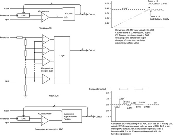
3.2.1. Tracking ADC
The tracking ADC has a comparator, a counter, and a digital-to-analog converter. The comparator compares the input voltage to the DAC output voltage. If the input is higher than the DAC voltage, the counter counts up. If the input is lower than the DAC voltage, the counter counts down.
The DAC input is connected to the counter output. Say the reference voltage is 5V. This would mean that the converter could convert voltages between 0V and 5V. If the most significant bit of the DAC input is ‘‘1,’’ the output voltage is 2.5V. If the next bit is ‘‘1,’’ 1.25V is added, making the result 3.75V. Each successive bit adds half the voltage of the previous bit, so the DAC input bits correspond to the voltages in Table 3.5.
Table 3.5. DAC input bits
| Bit: | Bit 7 | Bit 6 | Bit 5 | Bit 4 | Bit 3 | Bit 2 | Bit 1 | Bit 0 |
| Volts: | 2.5 | 1.25 | 0.625 | 0.3125 | 0.156 | 0.078 | 0.039 | 0.0195 |
Figure 3.3 shows how the tracking ADC resolves an input voltage of 0.37V. The counter starts at 0, so the comparator output is high. The counter counts up once for every clock pulse, stepping the DAC output voltage up. When the counter passes the binary value that represents the input voltage, the comparator output will switch and the counter will count down. The counter will eventually oscillate around the value that represents the input voltage.
The primary drawback to the tracking ADC is speed—a conversion can take up to 256 clocks for an 8-bit output, 1024 clocks for a 10-bit value, and so on. In addition, the conversion speed varies with the input voltage. If the voltage in this example were 0.18V, the conversion would take only half as many clocks as the 0.37-V example.
The maximum clock speed of a tracking ADC depends on the propagation delay of the DAC and the comparator. After every clock, the counter output has to propagate through the DAC and appear at the output. The comparator then takes some amount of time to respond to the change in DAC voltage, producing a new up/down control input to the counter. Tracking ADCs are not commonly available; in looking at the parts available from Analog Devices, Maxim, and Burr-Brown (all three are manufacturers of ADC components), not one tracking ADC is shown. This only makes sense: A successive approximation ADC with the same number of bits is faster. However, there is one case where a tracking ADC can be useful; if the input signal changes slowly with respect to the sampling clock, a tracking ADC may produce an output in fewer clocks than a successive approximation ADC. However, since there are no commercial tracking ADCs available, a tracking ADC would have to be built from discrete hardware.
3.2.2. Flash ADC
The flash ADC is the fastest type available. A flash ADC has one comparator per voltage step. A 4-bit ADC will have 16 comparators, an 8-bit ADC will have 256 comparators. One input of all the comparators is connected to the input to be measured. The other input of each comparator is connected to one point in a string of resistors. As you move up the resistor string, each comparator trips at a higher voltage. All of the comparator outputs connect to a block of logic that determines the output based on which comparators are low and which are high.
The conversion speed of the flash ADC is the sum of the comparator delays and the logic delay (the logic delay is usually negligible). Flash ADCs are very fast but take enormous amounts of IC real estate to implement. Because of the number of comparators required, they tend to be power hogs, drawing significant current. A 10-bit flash ADC IC may use half an amp.
3.2.3. Successive Approximation Converter
The successive approximation converter is similar to the tracking ADC in that a DAC/counter drives one side of a comparator and the input drives the other. The difference is that the successive approximation register performs a binary search instead of just counting up or down by 1. As shown in Figure 3.3, say we start with an input of 3V, using a 5-V reference. The successive approximation register would perform the conversion as follows:
- Set MSB of SAR, DAC voltage = 2.5V
- Comparator output high, so leave MSB set
- Result = 1000 0000
- Set bit 6 of SAR, DAC voltage = 3.75V (2.5 + 1.25)
- Comparator output low, reset bit 6
- Result = 1000 0000
- Set bit 5 of SAR, DAC voltage = 3.125V (2.5 + 0.625)
- Comparator output low, reset bit 5
- Result = 1000 0000
- Set bit 4 of SAR, DAC voltage = 2.8125V (2.5 + 0.3125)
- Comparator output high, leave bit 4 set
- Result = 1001 0000
- Set bit 3 of SAR, DAC voltage = 2.968V (2.8125 + 0.15625)
- Comparator output high, leave bit 3 set
- Result = 1001 1000
- Set bit 2 of SAR, DAC voltage = 3.04V (2.968 + 0.078125)
- Comparator output low, reset bit 2
- Result = 1001 1000
- Set bit 1 of SAR, DAC voltage = 3.007V (2.8125 + 0.039)
- Comparator output low, reset bit 1
- Result = 1001 1000
- Set bit 0 of SAR, DAC voltage = 2.988V (2.8125 + 0.0195)
- Comparator output high, leave bit 0 set
- Final result = 10011001
Using the 0-to-5-V, 8-bit DAC, this corresponds to
![]()
This is not exactly 3V, but it is as close as we can get with an 8-bit converter and a 5-V reference.
An 8-bit successive approximation ADC can do a conversion in eight clocks, regardless of the input voltage. More logic is required than for the tracking ADC, but the conversion speed is consistent and usually faster.
3.2.4. Dual-Slope (Integrating) ADC
A dual-slope converter (Figure 3.4) uses an integrator followed by a comparator, followed by counting logic. The integrator input is first switched to the input signal, and the integrator output charges toward the input voltage. After a specified number of clock cycles, the integrator input is switched to a reference voltage (VREF1 in Figure 3.4) and the integrator charges down toward this value.
Figure 3.4. Dual-slope ADC.
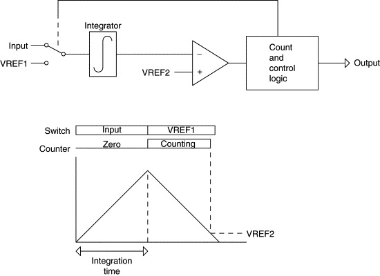
When the switch occurs to VREF1, a counter is started, and it counts using the same clock that determined the original integration time. When the integrator output falls past a second reference voltage (VREF2 in Figure 3.4), the comparator output goes high, the counter stops, and the count represents the analog input voltage. Higher input voltages will allow the integrator to charge to a higher voltage during the input time, taking longer to charge down to VREF2, and resulting in a higher count at the output. Lower input voltages result in a lower integrator output and a smaller count.
A simpler integrating converter, the single-slope, runs the counter while charging up and stops counting when a reference voltage is reached (instead of charging for a specific time). However, the single-slope converter is affected by clock accuracy. The dual-slope design eliminates clock accuracy problems because the same clock is used for charging and incrementing the counter. Note that clock jitter or drift within a single conversion will affect accuracy. The dual-slope converter takes a relatively long time to perform a conversion, but the inherent filtering action of the integrator eliminates noise.
3.2.5. Sigma-Delta
Before describing the sigma-delta converter, we need to look at how oversampling works, because it is key to understanding the sigma-delta architecture. Figure 3.5 shows a noisy 3-V signal, with 0.2-V peak-to-peak of noise. As shown in the figure, we can sample this signal at regular intervals. Four samples are shown in the figure; by averaging these we can filter out the noise:
![]()
Figure 3.5. Oversampling.

Obviously this example is a little contrived, but it illustrates the point. If our system can sample the signal four times faster than data are actually needed, we can average four samples. If we can sample 10 times faster, we can average 10 samples for an even better result. The more samples we can average, the closer we get to the actual input value. The catch, of course, is that we have to run the ADC faster than we actually need the data and must have software to do the averaging.
Figure 3.6 shows how a sigma-delta converter works. The input signal passes through one side of a differential amp, through a low-pass filter (integrator), and on to a comparator. The output of the comparator drives a digital filter and a 1-bit DAC. The DAC output can switch between +V and −V. In the example shown in Figure 3.6, the +V is 0.5V, and the −V is −0.5V. The output of the DAC drives the other side of the differential amp, so the output of the differential amp is the difference between the input voltage and the DAC output. In the example shown, the input is 0.3V, so the output of the differential amp is either 0.8V (when the DAC output is −0.5V) or −0.2V (when the DAC output is 0.5V).
Figure 3.6. Sigma-delta ADC.
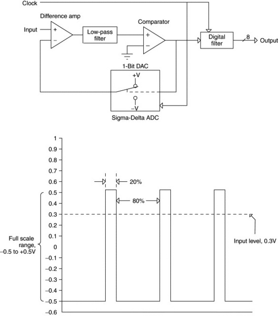
The output of the low-pass filter drives one side of the comparator, and the other side of the comparator is grounded. So any time the filter output is above ground, the comparator output will be high, and any time the filter output is below ground, the comparator output will be low. The thing to remember is that the circuit tries to keep the filter output at 0V.
As shown in Figure 3.6, the duty cycle of the DAC output represents the input level; with an input of 0.3V (80% of the −0.5 to 0.5V range), the DAC output has a duty cycle of 80%. The digital filter converts this signal to a binary digital value.
The input range of the sigma-delta converter is the plus-and-minus DAC voltage. The example in Figure 3.6 uses 0.5 and −0.5V for the DAC, so the input range is −0.5V to 0.5V, or 1V total. For ±1-V DAC outputs, the range would be ±1V, or 2V total.
The primary advantage of the sigma-delta converter is high resolution. Because the duty cycle feedback can be adjusted with a resolution of one clock, the resolution is limited only by the clock rate. Faster clock equals higher resolution.
All of the other types of ADCs use some type of resistor ladder or string. In the flash ADC the resistor string provides a reference for each comparator. On the tracking and successive approximation ADCs, the ladder is part of the DAC in the feedback path. The problem with the resistor ladder is that the accuracy of the resistors directly affects the accuracy of the conversion result. Although modern ADCs use very precise, laser-trimmed resistor networks (or sometimes capacitor networks), there are still some inaccuracies in the resistor ladders. The sigma-delta converter does not have a resistor ladder; the DAC in the feedback path is a single-bit DAC, with the output swinging between the two reference end points. This provides a more accurate result.
The primary disadvantage of the sigma-delta converter is speed. Because the converter works by oversampling the input, the conversion takes many clocks. For a given clock rate, the sigma-delta converter is slower than other converter types. Or, to put it another way, for a given conversion rate, the sigma-delta converter requires a faster clock.
Another disadvantage of the sigma-delta converter is the complexity of the digital filter that converts the duty cycle information to a digital output word. Single-IC sigma-delta converters have become more commonly available, with the ability to add a digital filter or DSP to the IC die.
3.2.6. Half-Flash
Figure 3.7 shows a block diagram of a half-flash converter. This example implements an 8-bit ADC with 32 comparators instead of 256. The half-flash converter has a 4-bit (16 comparators) flash converter to generate the MSB of the result. The output of this flash converter then drives a 4-bit DAC to generate the voltage represented by the 4-bit result. The output of the DAC is subtracted from the input signal, leaving a remainder that is converted by another 4-bit flash to produce the four LSBs of the result.
Figure 3.7. Half-flash converter.

If the converter shown in Figure 3.7 were a 0–5-V converter converting a 3.1-V input, then the conversion would look like this:
- Upper flash converter output = 9
- DAC output = 2.8125V(9 × 16 × 19.53 mV)
- Subtracter output = 3.1V − 2.8125V = 0.2875V
- Lower flash converter output = E (hex)
- Final result = 9E (hex), 158 (decimal)
Half-flash converters can also use three stages instead of two; a 12-bit converter might have three stages of 4 bits each. The result of the four MSBs is subtracted from the input voltage and applied to the middle 4-bit state. The result of the middle stage is subtracted from its input and applied to the least significant 4-bit stage. A half-flash converter is slower than an equivalent flash converter, but uses fewer comparators, so it draws less current.
3.3. ADC Comparison
Figure 3.8 shows the range of resolutions available for integrating, sigma-delta, successive approximation, and flash converters. The maximum conversion speed for each type also is shown. As you can see, the speed of available sigma-delta ADCs reaches into the range of the SAR ADCs, but is not as fast as even the slowest flash ADCs. What these charts do not show is trade-offs between speed and accuracy. For instance, although you can get SAR ADCs that range from 8 to 16 bits, you will not find the 16-bit version to be the fastest in a given family of parts. The fastest flash ADC will not be the 12-bit part, it will be a 6- or 8-bit part.
Figure 3.8. ADC comparison.

These charts are snapshots of the current state of the technology. As CMOS processes have improved, SAR conversion times have moved from tens of microseconds to microseconds to tens of nanoseconds. Not all technology improvements affect all types of converters; CMOS process improvements speed up all families of converters, but the ability to put increasingly sophisticated DSP functionality on the ADC chip does not improve SAR converters. It does improve sigma-delta types.
3.4. Sample and Hold
ADC operation is straightforward when a DC signal is being converted. What happens when the signal is changing? Figure 3.9 shows a successive-approximation ADC attempting to convert a changing input. When the ADC starts the conversion, the input voltage is 2.3V. This should result in an output code of 117 (decimal) or 75 (hex). The SAR register sets the MSB, making the internal DAC voltage 2.5V. Because the signal is below 2.5V, the SAR resets bit 7 and sets bit 6 on the next clock. The ADC ‘‘chases’’ the input signal, ending up with a final result of 12710(7F16). The actual voltage at the end of the conversion is 2.8V, corresponding to a code of 14310(8F16).
Figure 3.9. ADC inaccuracy caused by a changing input.
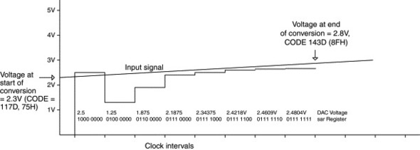
The final code out of the ADC (127d) corresponds to a voltage of 2.48V. This is neither the starting voltage (2.3V) nor the ending voltage (2.8V). This example used a relatively fast input to show the effect; a slowly changing input has the same effect, but the error is smaller. One way to reduce these errors is to place a low-pass filter ahead of the ADC. The filter parameters are selected to ensure that the ADC input does not change appreciably within a conversion cycle.
Another way to handle changing inputs is to add a sample-and-hold (S/H) circuit ahead of the ADC. Figure 3.10 shows how a sample-and-hold circuit works. The S/H circuit has an analog (solid state) switch with a control input. When the switch is closed, the input signal is connected to the hold capacitor and the output of the buffer follows the input. When the switch is open, the input is disconnected from the capacitor.
Figure 3.10. Sample-and-hold circuit.

Figure 3.10 shows the waveform for S/H operation. A slowly rising signal is connected to the S/H input. While the control signal is low (sample), the output follows the input. When the control signal goes high (hold), disconnecting the hold capacitor from the input, the output stays at the value the input had when the S/H switched to hold mode. When the switch closes again, the capacitor charges quickly and the output again follows the input. Typically, the S/H will be switched to hold mode just before the ADC conversion starts, and switched back to sample mode after the conversion is complete.
In a perfect world, the hold capacitor would have no leakage and the buffer amplifier would have infinite input impedance, so the output would remain stable forever. In the real world, the hold capacitor will leak and the buffer amplifier input impedance is finite, so the output level will slowly drift down toward ground as the capacitor discharges.
The ability of an S/H to maintain the output in hold mode is dependent on the quality of the hold capacitor, the characteristics of the buffer amplifier (primarily input impedance), and the quality of the sample-and-hold switch (real electronic switches have some leakage when open). The amount of drift exhibited by the output when in hold mode, called the droop rate, is specified in millivolts per second, microvolts per microsecond, or millivolts per microsecond.
A real S/H also has finite input impedance, because the electronic switch is not perfect. This means that, in sample mode, the hold capacitor is charged through some resistance. This limits the speed with which the S/H can acquire an input. The time that the S/H must remain in sample mode in order to acquire a full-scale input, called the acquisition time, is specified in nanoseconds or microseconds.
Because there is some impedance in series with the hold capacitor when sampling, the effect is the same as a low-pass R-C filter. This limits the maximum frequency the S/H can acquire. This is called the full power bandwidth, specified in kilohertz or megahertz.
As mentioned, the electronic switch is imperfect and some of the input signal appears at the output, even in hold mode. This is called feedthrough, and is typically specified in decibles.
The output offset is the voltage difference between the input and the output. S/H data sheets typically show a hold mode offset and sample mode offset, in millivolts.
3.5. Real Parts
Real ADC ICs come with a few real-world limitations and some added features.
3.5.1. Input Levels
The examples so far have concentrated on ADCs with a 0–5-V input range. This is a common range for real ADCs, but many of them operate over a wider range of voltages. The Analog Devices AD570 has a 10-V input range. The part can be configured so that this 10-V range is either 0 to 10V or −5V to +5V, using one pin. Of course, having a negative input voltage range implies that the ADC will need a negative voltage supply. Other common input voltage ranges are ±2.5V and ±3V.
With the trend toward lower-powered devices and small consumer equipment, the trend in ADC devices is to lower-voltage, single-supply operation. Traditional single-supply ADCs have operated from +5V and had an input range between 0 and 5V. Newer parts often operate at 3.3 or 2.7V and have an input range somewhere between 0V and the supply.
3.5.2. Internal Reference
Many ADCs provide an internal reference voltage. The Analog Devices AD872 is a typical device with an internal 2.5-V reference. The internal reference voltage is brought out to a pin and the reference input to the device is also connected to a pin. To use the internal reference, the two pins are connected together. To use your own external reference, connect it to the reference input instead of the internal reference.
3.5.3. Reference Bypassing
Although the reference input is usually high impedance with low DC current requirements, many ADCs will draw current from the reference briefly while a conversion is in process. This is especially true of successive approximation ADCs, which draw a momentary spike of current each time the analog switch network is changed. Consequently, most ADCs require that the reference input be bypassed with a capacitor of 0.1 μf or so.
3.5.4. Internal S/H
Many ADCs, such as the Maxim MAX191, include an internal S/H. An ADC with an internal S/H may have a separate pin that controls whether the S/H is in sample or hold mode, or the switch to hold mode may occur automatically when a conversion is started.
3.6. Microprocessor Interfacing
3.6.1. Output Coding
The examples used so far have been based on binary codes, where each bit in the result represents a voltage value and the sum of these voltages in the output word is the analog input voltage value. Some ADCs produce two's complement outputs, where a negative voltage is represented by a negative two's complement value. A few ADCs output values in BCD. Obviously this requires more bits for a given range; a 12-bit binary output can represent values from 0 to 4095, but a 12-bit BCD output can only represent values from 0 to 999.
3.6.2. Parallel Interfaces
ADCs come in a variety of interfaces, intended to operate with multiple processors. Some parts include more than one type of interface to make them compatible with as many processor families as possible.
The Maxim MAX151 is a typical 10-bit ADC with an 8-bit “universal” parallel interface. As shown in Figure 3.11, the processor interface on the MAX151 has 8 data bits, a chip select (–CS), a read strobe (–RD), and a –BUSY output. The MAX151 includes an internal S/H. On the falling edge of –RD and –CS, the S/H is placed into hold mode and a conversion is started. If –CS and –RD do not go low at the same time, the last falling edge starts a conversion. In most systems, –CS is connected to an address decode and will go low before –RD. As soon as the conversion starts, the ADC drives –BUSY low (active). –BUSY remains low until the conversion is complete.
Figure 3.11. Maxim MAX151 interface.
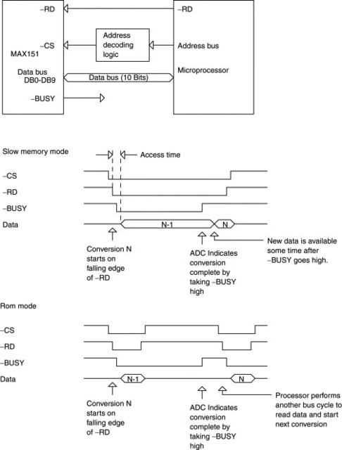
In the first mode of operation, which Maxim calls Slow Memory Mode, the processor waits, holding –RD and –CS low, until the conversion is complete. In such a system, the –BUSY signal would typically be connected to the processor –RDY or –WAIT signal. This holds the processor in a wait state until the conversion is complete. The maximum conversion time for the MAX151 is 2.5 μs.
The second mode of operation is called ROM mode. In this mode, the processor performs a read cycle, which places the S/H in hold mode and starts a conversion. During this read the processor reads the results of the previous conversion. The –BUSY signal is not used to extend the read cycle. Instead, –BUSY is connected to an interrupt or is polled by the processor to indicate when the conversion is complete. When –BUSY goes high, the processor does another read to get the result and start another conversion. Although the data sheets refer to two different modes of operation, the ADC works the same way in both cases:
- Falling edge of –RD and –CS starts a conversion
- Current result is available on bus after read access time has elapsed
- As long as –RD and –CS stay low, current result remains available on bus
- When conversion completes, new conversion data is latched and available to the processor; if –RD and –CS are still low, this data replaces result of previous conversion on bus
The MAX151 is designed to interface to most microprocessors. Actually interfacing to a specific processor requires analysis of the MAX151 timing and how it relates to the microprocessor timing.
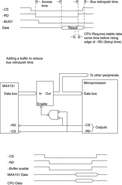
3.6.3. Data Access Time
The MAX151 specifies a maximum access time of 180 ns over the full temperature range (see Figure 3.12). This means that the result of a conversion will be available on the bus no more than 180 ns after the falling edge of –RD (assuming –CS is already low when –RD goes low). The processor will need the data to be stable some time before the rising edge of –RD. If there is a data bus buffer between the MAX151 and the processor, the propagation delay through the buffer must be included. This means that the processor bus cycle (the time that –RD is low) must be at least as long as the access time of the MAX151, plus the processor data setup time, plus any bus buffer delays.
Figure 3.12. MAX151 data access and bus relinquish timing.
3.6.4. –BUSY Output
The –BUSY output of the MAX151 goes low a maximum of 200 ns after the falling edge of –RD. This is too long for the signal to directly drive most microprocessors if you want to use the slow memory mode. Most microprocessors require that the –RDY or –WAIT signal be driven low earlier than this in the bus cycle. Some require the wait request signal to be low one clock after –RD goes low. The only solution to this problem is to artificially insert wait states to the bus cycle until the –BUSY signal goes low. Some microprocessors, such as the 80188 family, have internal wait-state generators that can add wait states to a bus cycle. The 80188 wait-state generator can be programmed to add zero, one, two, or three wait states.
As shown in Figure 3.12, in slow memory mode, the –BUSY signal goes high just before the new conversion result is available; according to the data sheet, this time is a maximum of 50 ns. For some processors, this means that the wait request must be held active for an additional clock cycle after –BUSY goes high to ensure that the correct data is read at the end of the bus cycle.
3.6.5. Bus Relinquish
The MAX151 has a maximum bus relinquish time of 100 ns. This means that the MAX151 can drive the data bus up to 100 ns after the –RD signal goes high. If the processor tries to start another cycle immediately after reading the MAX151 result, this may result in bus contention. A typical example would be the 80186 processor, which multiplexes the data bus with the address bus; at the start of a bus cycle, the data bus is not tristated, but the processor drives the address onto the data bus. If the MAX151 is still driving the bus, this can result in an incorrect bus address being latched. The solution to this problem is to add a data bus buffer between the MAX151 and the processor. The buffer inputs are connected to the MAX151 data bus outputs, and the buffer outputs are connected to the processor data bus. The buffer is turned on when –RD and –CS are both low and turned off when either goes high. Although the MAX151 will continue to drive the buffer inputs, the outputs will be tristated and so will not conflict with the processor data bus. A buffer may also be required if you are interfacing to a microprocessor that does not multiplex the data lines but does have a very high clock rate. In this case, the processor may start the next cycle before the MAX151 has relinquished the bus. A typical example would be a fast 80960-family processor, which we look at later in the chapter.
3.6.6. Coupling
The MAX151 has an additional specification, not found on some ADCs, that involves coupling of the bus control signals into the ADC. Because modern ADCs are built as monolithic ICs, the analog and digital portions share some internal components such as the power supply pins and the substrate on which the IC die is constructed. It is sometimes difficult to keep the noise generated by the microprocessor data bus and control signals from coupling into the ADC and affecting the result of a conversion. To minimize the effect of coupling, the MAX151 has a specification that the –RD signal be no more than 300 ns wide when using ROM mode. This prevents the rising edge of –RD from affecting the conversion.
3.6.7. Delay between Conversions
When the MAX151 S/H is in sampling mode, the hold capacitor is connected to the input. This capacitance is about 150 pf. When a conversion starts, this capacitor is disconnected from the input. When a conversion ends, the capacitor is again connected to the input, and it must charge up to the value of the input pin before another conversion can start. In addition, there is an internal 150-Ω resistor in series with the input capacitor. Consequently, the MAX151 specifies a delay between conversions of at least 500 ns if the source impedance driving the input is less than 50Ω. If the source impedance is more than 1 KΩ, the delay must be at least 1.5 μs. This delay is the time from the rising edge of –BUSY to the falling edge of –RD.
3.6.8. LSB Errors
In theory, of course, an infinite amount of time is required for the capacitor to charge up, because the charging curve is exponential and the capacitor never reaches the input voltage. In practice, the capacitor does stop charging. More important, the capacitor only has to charge to within 1 bit (called one LSB) of the input voltage; for a 10-V converter with a ±4-V input range, this is 8V/1024, or 7.8 mV. To simplify the concept, errors that fall within one bit of resolution have no effect on conversion accuracy. The other side of that coin is that the accumulation of errors (op-amp offsets, gain errors, etc.) cannot exceed one bit of resolution or they will affect the result.
3.7. Clocked Interfaces
Interfacing the MAX151 to a clocked bus, such as that implemented on the Intel 80960 family, is shown in Figure 3.13. Processors such as the 960 use a clock-synchronized bus without an –RD strobe. Data is latched by the processor on a clock edge, rather than on the rising edge of a control signal such as –RD. These buses are often implemented on very fast processors and are usually capable of high-speed burst operation.
Figure 3.13. Interfacing to a clocked microprocessor bus.
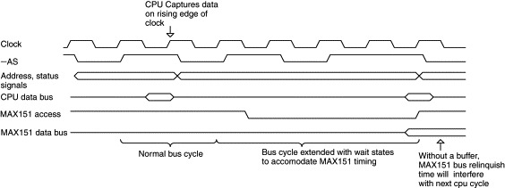
Shown in Figure 3.13 is a normal bus cycle without wait states. This bus cycle would be accessing a memory or peripheral able to operate at the full bus speed. The address and status information are provided on one clock, and the CPU reads the data on the next clock.
Following this cycle is an access to the MAX151. As can be seen, the MAX151 is much slower than the CPU, so the bus cycle must be extended with wait states (either internally or externally generated). This diagram is an example; the actual number of wait states that must be added depends on the processor clock rate. The bus relinquish time of the MAX151 will interfere with the next CPU cycle, so a buffer is necessary. Finally, because the CPU does not generate an –RD signal, one must be synthesized by the logic that decodes the address bus and generates timing signals to memory and peripherals. The normal method of interfacing an ADC like this to a fast processor is to use the ROM mode. Slow memory mode holds the CPU in a wait state for a long time—the 2.5 μs conversion time of the MAX151 would be 82 clocks on a 33-MHz 80960. This is time that could be spent executing code.
3.8. Serial Interfaces
Many ADCs use a serial interface to connect to the microprocessor. This has the advantage of providing a processor-independent interface that does not affect processor wait states, bus hold times, or clock rates. The primary disadvantage is speed, because the data must be transferred one bit at a time.
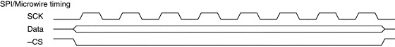
3.8.1. SPI/Microwire
SPI is a serial interface that uses a clock, chip select, data in, and data out bits. Data is read from a serial ADC a bit at a time (Figure 3.14). Each device on the SPI bus requires a separate –CS signal.
Figure 3.14. SPI bus.
The Maxim MAX1242 is a typical SPI ADC. The MAX1242 is a 10-bit successive approximation ADC with an internal S/H, in an eight-pin package. Figure 3.15 shows the MAX1242 interface timing. The falling edge of −CS starts a conversion, which takes a maximum of 7.5 μs. When –CS goes low, the MAX1242 drives its data output pin low. After the conversion is complete, the MAX1242 drives the data output pin high. The processor can then read the data a bit at a time by toggling the clock line and monitoring the MAX1242 data output pin. After the 10 bits are read, the MAX1242 provides two subbits, S1 and S0. If further clock transitions occur after the 13 clocks, the MAX1242 outputs zeros.
Figure 3.15. Maxim MAX1242 interface.

Figure 3.15 shows how a MAX1242 would be connected to a microcontroller with an on-chip SPI/Microwire interface. The SCLK signal goes to the SPI SCLK signal on the microcontroller, and the MAX1242 DOUT signal connects to the SPI data input pin on the microcontroller. One of the microcontroller port bits generates the –CS signal to the MAX1242. Note that the –CS signal starts the conversion and must remain low until the conversion is complete. This means that the SPI bus is unavailable for communicating with other peripherals until the conversion is finished and the result has been read. If there are interrupt service routines that communicate with SPI devices in the system, they must be disabled during the conversion. To avoid this problem, the MAX1242 could communicate with the microcontroller over a dedicated SPI bus. This would use three more pins on the microcontroller. Since most microcontrollers that have on-chip SPI have only one, the second port would have to be implemented in software.
Finally, it is possible to generate an interrupt to the microcontroller when the ADC conversion is complete. An extra connection is shown in Figure 3.15, from the MAX1242 DOUT pin to an interrupt on the microcontroller. When –CS is low and the conversion is completed, DOUT will go high, interrupting the microcontroller. To use this method, the firmware must disable or otherwise ignore the interrupt except when a conversion is in process.
Another ADC with an SPI-compatible interface is the Analog Devices AD7823. Like the MAX1242, the AD7823 uses three pins: SCLK, DOUT, and –CONVST. The AD7823 is an 8-bit successive approximation ADC with internal S/H. A conversion is started on the falling edge of –CONVST and takes 5.5 μs. The rising edge of –CONVST enables the serial interface.
Unlike the MAX1242, the AD7823 does not drive the data pin until the microcontroller reads the result, so the SPI bus can be used to communicate with other devices while the conversion is in process. However, there is no indication to the microprocessor when the conversion is complete—the processor must start the conversion, then wait until the conversion has had time to complete before reading the result. One way to handle this is with a regular timer interrupt; on each interrupt, the result of the previous conversion is read and a new conversion is started.
3.8.2. I2C Bus
The I2C bus uses only two pins: SCL (SCLock) and SDA (SDAta). SCL is generated by the processor to clock data into and out of the peripheral device. SDA is a bidirectional line that serially transmits all data into and out of the peripheral. The SDA signal is open collector, so several peripherals can share the same two-wire bus.
When sending data, the SDA signal is allowed to change only while SCL is in the low state. Transitions on the SDA line while SCL is high are interpreted as start and stop conditions. If SDA goes low while SCL is high, all peripherals on the bus will interpret this as a START condition. SDA going high while SCL is high is a STOP or END condition. Figure 3.16 illustrates a typical data transfer. The processor initiates the START condition and then sends the peripheral address, which is 7 bits long, and tells the devices on the bus which one is to be selected. This is followed by a read/write bit (1 for read, 0 for write).
Figure 3.16. I2C timing.

After the read/write bit, the processor programs the I/O pin connected to the SDA bit to be an input and clocks an acknowledge bit in. The selected peripheral will drive the SDA line low to indicate that it has received the address and read/write information.
After the acknowledge bit, the processor sends another address, which is the internal address within the peripheral that the processor wants to access. The length of this field varies with the peripheral. After this is another acknowledge, then the data is sent. For a write operation, the processor clocks out 8 data bits, and for a read operation, the processor treats the SDA pin as an input and clocks in 8 bits. After the data comes another acknowledge.
Some peripherals permit multiple bytes to be read or written in one transfer. The processor repeats the data/acknowledge sequence until all the bytes are transferred. The peripheral will increment its internal address after each transfer.
One drawback to the I2C bus is speed—the clock rate is limited to about 100 KHz. A newer fast-mode I2C bus that operates to 400 Kbits/s is also available, and a high-speed mode that goes to 3.4 Mbits/s is also available. High-speed and fast-mode buses both support a 10-bit address field, so up to 1024 locations can be addressed. High-speed and fast-mode devices are capable of operating in the older system, but older peripherals are not useable in a higher-speed system. The faster interfaces have some limitations, such as the need for active pull-ups and limits on bus capacitance. Of course, the faster modes of operation require hardware support and are not suitable for a software-controlled implementation.
A typical ADC that uses I2C is the Philips PCF8591. This part includes both an ADC and a DAC. Like many I2C devices, the 8591 has three addressing pins: A0, A1, and A2. These can be connected to either “1” or “0” to select which address the device responds to. When the peripheral address is decoded, the PCF8591 will respond to address 1001xxx, where xxx matches the value of the A2, A1, and A0 pins. This allows up to eight PCF8591 devices to share a single I2C bus.
3.8.3. SMBus
SMBus is a variation on I2C, defined by Intel in 1995. I2C is primarily defined by hardware and varies somewhat from one device to the next, but SMBus defines the bus as more of a network interface between a processor and its peripherals. The SMBus specification defines things such as power-down operation of devices (no bus loading) and operating voltage range (3–5V) that all devices must meet. The primary difference between SMBus and I2C is that SMBus defines a standard set of read and write protocols, rather than leaving these specifics up to the IC manufacturers.
3.8.4. Proprietary Serial Interfaces
Some ADCs have proprietary interfaces. The Maxim MAX1101 is a typical device. This is an 8-bit ADC that is optimized for interfacing to CCDs. The MAX1101 uses four pins: MODE, LOAD, DATA, and SCLK. The MODE pin determines whether data is being written or read (1 = read, 0 = write). The DATA pin is a bidirectional signal, the SCLK signal clocks data into and out of the device, and the LOAD pin is used after a write to clock the write data into the internal registers. The clocked serial interface of the MAX1101 is similar to SPI, but because there is no chip select signal, multiple devices cannot share the same data/clock bus. Each MAX1101 (or similar device) needs four signals from the processor for the interface.
Many proprietary serial interfaces are intended for use with microcontrollers that have on-chip hardware to implement synchronous serial I/O. The 8031 family, for example, has a serial interface that can be configured as either an asynchronous interface or as a synchronous interface. Many ADCs can connect directly to these types of microprocessors. The problem with any serial interface on an ADC is that it limits conversion speed. In addition, the type of interface limits speed as well. Because every I2C exchange involves at least 20 bits, an I2C device will never be as fast as an equivalent SPI or proprietary device. For this reason, many more ADCs are available with SPI/Microwire than with I2C interfaces.
The required throughput of the serial interface drives the design. If you need a conversion speed of 100,000 8-bit samples per second and you plan to implement an SPI-type interface in software, then your processor will not be able to spend more than 1/(100,000 × 8) or 1.25 μs transferring each bit. This may be impractical if the processor has any other tasks to perform, so you may want to use an ADC with a parallel interface or choose a processor with hardware support for the SPI.
As mentioned in Section 3.1, the bandwidth of the bus must be considered as well as the throughput of the processor. If there are multiple devices on the SPI bus, then you have to be sure the bus can support the total throughput required of all the devices. Of course, the processor has to keep up with the overall data rate as well.
3.9. Multichannel ADCs
Many ADCs are available with multiple channels, anywhere from two to eight. The Analog Devices AD7824 is a typical device, with eight channels. The AD7824 contains a single 8-bit ADC and an 8-channel analog multiplexer. The microprocessor interface to the AD7824 is similar to the Maxim MAX151, but with the addition of three address lines (A0–A2) to select which channel is to be converted. Like the MAX151, the AD7824 may be used in a mode in which the microprocessor starts a conversion and is placed into a wait state until the conversion is complete. The microprocessor can also start a conversion on any channel (by reading data from that channel), then wait for the conversion to complete and perform another read to get the result. The AD7824 also provides an interrupt output that indicates when a conversion is complete.
3.10. Internal Microcontroller ADCs
Many microcontrollers contain on-chip ADCs. Typical devices include the Microchip PIC167C7xx family and the Atmel AT90S4434. Most microcontroller ADCs are successive approximation because this gives the best trade-off between speed and IC real estate on the microcontroller die.
The PIC16C7xx microcontrollers contain an 8-bit successive approximation ADC with analog input multiplexers. The microcontrollers in this family have from four to eight channels. Internal registers control which channel is selected, start of conversion, and so on. Once an input is selected, there is a settling time that must elapse to allow the S/H capacitor to charge before the A/D conversion can start. The software must ensure that this delay takes place.
3.10.1. Reference Voltage
The Microchip devices allow you to use one input pin as a reference voltage. This is normally tied to some kind of precision reference. The value read from the A/D converter after a conversion is
![]()
The Microchip parts also permit the reference voltage to be internally set to the supply voltage, which permits the reference input pin to be another analog input. In a 5-V system, this means that Vref is 5V. So measuring a 3.2-V signal would produce the following result:
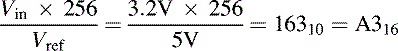
However, the result is dependent on the value of the 5-V supply. If the supply voltage is high by 1%, it has a value of 5.05V. Now the value of the A/D conversion will be
![]()
So a 1% change in the supply voltage causes the conversion result to change by one count. Typical power supplies can vary by 2 or 3%, so power supply variations can have a significant effect on the results. The power supply output can vary with loading, temperature, AC input variations, and from one supply to the next.
This brings up an issue that affects all ADC designs: the accuracy of the reference. TheMaximMAX1242, which we have already looked at, uses an internal reference. The part can convert inputs from 0V to the reference voltage. The reference is nominally 2.5V, but it can vary between 2.47V and 2.53V. Converting a 2-V input at the extremes of the reference ranges gives the following result:
![]()
![]()
(Note: Multiplier is 1024 because the MAX1242 is a 10-bit converter.)
So the variation in the reference voltage from part to part can result in an output variation of 20 counts.
3.11. Codecs
The term codec has two meanings: It is short for compressor/decompressor or for coder/decoder. In general, a codec (either type) will have two-way operation; it can turn analog signals into digital and vice versa, or it can convert to and from some compression standard.
The National Semiconductor LM4546 is an audio codec intended to implement the sound system in a personal computer. It contains an internal 18-bit ADC and DAC. It also includes much of the audio-processing circuitry needed for three-dimensional PC sound. The LM4546 uses a serial interface to communicate with its host processor.
The National TP3054 is a telecom-type codec and includes ADC, DAC, filtering, and companding circuitry. The TP3054 also has a serial interface.
3.12. Interrupt Rates
The MAX151 can perform a conversion every 3.3 μs, or 300,000 conversions per second. Even a 33-MHz processor operating at one instruction per clock cycle can execute only 110 instructions in that time. The interrupt overhead of saving and restoring registers can be a significant portion of those instructions.
In some applications, the processor does not need to process every conversion. An example would be a design in which the processor takes four samples, averages them, and then does something with the average. In cases like this, using a processor with DMA capability can reduce the interrupt overhead. The DMA controller is programmed to read the ADC at regular intervals, based on a timer (the ADC has to be a type that starts a new conversion as soon as the previous result is read). After all the conversions are complete, the DMA controller interrupts the processor. The accumulated ADC data is processed and the DMA controller is programmed to start the sequence over. Processors that include on-chip DMA controllers include the 80186 and the 386EX.
3.13. Dual-Function Pins on Microcontrollers
If you work with microcontrollers, you sometimes find that you need more I/O pins than your microcontroller has. This is most often a problem when working with smaller devices, such as the 8-pin Atmel ATtiny parts or the 20- and 28-pin Atmel AVR and Microchip PIC devices. In some cases, you can make an analog input double as an output or make it handle two inputs. Figure 3.17A shows how an analog input can also control two outputs. In this case, the analog input is connected to a 2.5-V reference diode. A typical use for this design would be in an application where you are using the 5-V supply as the ADC reference, but you want to correct the readings for the actual supply value. A precise 2.5-V reference permits you to do this, because you know that the value of the reference should read as 80 (hex) if the power supply is exactly 5V.
Figure 3.17. Dual-function pins.

The pin on the microcontroller is also tied to the inputs of two comparators. A voltage divider sets the noninverting input of comparator A at 3V and the inverting input of comparator B at 2V. By configuring the pin as an analog input, the reference value can be read. If the pin is then configured as a digital output and set low, the output of comparator A will go low. If the pin is configured as a digital output and set high, the output of comparator B will go low. Of course, this scheme works only if the comparator outputs drive signals that never need to both be low at the same time. The resistor values must be large enough that the microcontroller can source enough current to drive the pin high. This technique will also work for a digital-only I/O pin; instead of a 2.5-V reference, a pair of resistors is used to hold the pin at 2.5V when it is configured as an input.
Figure 3.17B shows how a single analog input can be used to read two switches. When both switches are open, the analog input will read 5V. When switch S1 is closed, the analog input will read 3.9V. When switch S2 is closed, the input will read 3.4V, and when both switches are closed, the input will read 2.9V. Instead of switches, you could also use this technique to read the state of open-collector or open-drain digital signals.
Figure 3.17C shows how a thermistor or other variable-resistance sensor can be combined with an output. The microcontroller pin is programmed as an analog input to read the temperature. When the pin is programmed as an output and driven high, the comparator output will go low. To make this work, the operating temperature range must be such that the voltage divider created by the thermistor and the pull-up resistor never brings the analog input above 3V. Like the example shown in Figure 3.17A, this circuit works best if the output is something that periodically changes state, so the software has a regular opportunity to read the analog input.
3.14. Design Checklist
- Be sure ADC bus interface is compatible with microprocessor timing. Pay particular attention to bus setup, hold, and min/max pulse width timings.
- If using SPI and an ADC that requires the bus to be inactive during conversion, ensure that the system will work with this limitation or provide a separate SPI bus for the ADC.
- If using an ADC that does not indicate when conversion is complete, ensure that software allows conversion to complete before reading result.
- Be sure reference accuracy meets requirements of the design.
- Bypass reference input as recommended by ADC manufacturer.
- Be sure the processor can keep up with the conversion rate.