Topic I: Overview of VLSI Design Methodology
“There is no single right way to design a chip, but there sure are many wrong ways.”
—Anonymous
This book describes the breadth of design, validation, and analysis steps associated with the development of an integrated circuit chip. Collectively, these steps are typically described as the overall methodology to be applied by the engineering teams throughout a chip design project. Some steps can be pursued concurrently, whereas others require successful completion of preceding steps as a project milestone before proceeding.
The design methodology encompasses more than just the steps to be followed. It also includes the policies in effect for chip hierarchy data management and the description of the model build configuration to represent the full chip logical and physical definitions. Each instance in the overall design configuration will be associated with a revision control system, with related version identifiers.
A key element of the design methodology is the application of electronic design automation (EDA) software tools used for each step, plus the software employed for design data management and revision control. Each step that invokes an EDA tool commonly executes a flow script, which ensures that the appropriate input files are available and requests the corresponding IT resources for job submission.
The design methodology includes specification of the various logical and physical data representations of the design, specifically the persistent file storage format(s) used for model input and output prior to and after tool execution. The design methodology is heavily dependent upon additional software scripts and utilities that transform the output data of one tool to be used as input to a subsequent tool. There are de facto and IEEE-sponsored file format standards that have been promoted by the EDA industry to simplify these tool interfaces.
An increasing trend is for an EDA vendor to provide multiple tools that share a common data model schema to represent the logical and physical design database. The EDA vendor typically offers a software application programming interface (API), consisting of a set of functions to query and update the model. The EDA vendor is also focused on optimizing the in-memory model data structures, especially for tools that execute in either a multi-threaded or distributed mode on large datasets.
An integrated EDA platform incorporating a data model with associated tools, an API, and a user interface for interactive steps offers considerable productivity improvements. For example, consider the methodology flow that analyzes I*R voltage drop on the supply and ground power distribution network, using estimates for the (static and dynamic) circuit currents throughout the chip (see Chapter 14, “Power Rail Voltage Drop Analysis”). The results of that analysis could be displayed in the interactive layout editor tool as a graphical overlay on the physical design, highlighting the layout coordinates where the voltage drop exceeds design margins. The layout engineer is thus able to more quickly identify where physical design updates are required. The EDA platform promotes tighter integration between tools and enables faster design optimization.
An important facet of the methodology is the management of the output result file(s) from exercising a flow. The suitability to move to the next step and the readiness to submit the final chip design for fabrication depend upon a review of the status of these results, especially any error and/or warning messages.
Methodologies are not static by any means. The general chip development project phases—design capture, functional validation, physical design, electrical analysis, and preparation for fabrication—have not changed substantially over the years. The aspects of the methodology that have evolved significantly are the specific tools and data model features used for each step, in response to new fabrication requirements and/or to improve flow throughput and designer productivity. For example, advanced fabrication processes require the photolithographic patterning of the most aggressive dimensions on the silicon wafer using multiple mask exposures per layer (see Section 1.2 in Chapter 1, “Introduction”). Thus, it is necessary to decompose the full set of layout shapes data for that layer into separate subsets that could be independently resolved with the photolithography exposure wavelength, as depicted in Figure I.1.
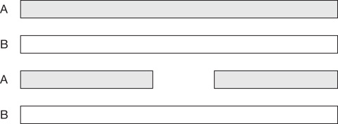
Figure I.1 Illustration of the multipatterning decomposition requirement for shapes data on a mask layer into A and B subsets. Fabrication of the design layer is implemented with multiple lithographic patterning and etch steps. For example, metal layer M1 could be fabricated using an “LELE” sequence, with two mask layer subsets.
New tools for multipatterning decomposition needed to be developed. New flows were scripted and added to the methodology to support the mask subset assignment to satisfy the optical resolution constraints. The increasing adoption of multiple power states during chip operation is another example of a requirement to be addressed by the methodology. Different power domains within the chip may change between active and sleep states at different times. There was a growing need for new tools to efficiently represent and validate the logical design of the power state sequences, especially across domain interfaces; implement and verify the unique (gated) power distribution to each of the domains; and analyze the electrical response to a power state transition. As the realization of power states broadly impacts tools across logical, physical, and electrical flows, the IEEE also engaged in an initiative to establish a new standard, defining the power format description semantics for all EDA vendors to use (see Section 7.6 in Chapter 7, “Logic Synthesis”). Methodologies continue to adapt to new design and fabrication requirements.
To address designer productivity and flow throughput concerns when faced with chip designs of increasing complexity, many tools are also being re-architected. A tool may support a shared-memory multi-threaded mode (e.g., to execute on a multi-core server) or a fully distributed mode (e.g., where the model data and/or tool algorithms are partitioned across multiple servers and execute under the coordination of a master process on a host server). A methodology team is often faced with decisions related to how to incorporate a completely new flow step or insert a new tool for an existing step when preparing for a chip design project.
Another area where the design methodology is changing relates to the increasing importance of chip-package co-design, a collaborative effort among chip and package technology engineering teams. The teams collectively develop the connectivity of power/ground distribution and high-performance signals through the package to the chip and analyze input/output signal behavior between the chip and the overall system.
The most important characteristic of a successful design methodology is planning. The resources and cost expenses allocated to a chip design project are fundamentally linked to the chosen methodology. In addition to addressing new requirements imposed by the fabrication process or supporting new design features, the methodology and project plan need to be in sync relative to the estimated time required to complete each flow step. That project schedule strongly depends on the following:
Engineering resources available
EDA tool license quantities available
IT resources available
Opportunities for the reuse of existing (logical and physical) functionality from previous designs (often described as reuse of intellectual property [IP])
The complexity associated with mapping existing IP functionality into new implementations to meet new specifications
These measures are linked to the hierarchical representation of the chip’s logical and physical models. The complete chip design is composed of an integration of hierarchical blocks, both a logical partitioning and a physical partitioning (see Chapter 3, “Hierarchical Design Decomposition”). The validation and analysis of the full chip is typically performed in a bottom-up manner. Individual blocks are functionally validated and analyzed separately (and, ideally, concurrently if sufficient resources are available). Upon successful exit of block-level flows and promotion of the block model, full-chip integration is pursued. The chip logic model is exercised against an extensive set of simulation testcases. Electrical analysis is also pursued, potentially using block abstracts to reduce the data volume of the full chip model.
The design methodology needs to provide the project team with resource estimates for tool/flow runtime and compute resources required to assist with the trade-offs on hierarchical partition size and complexity. Small blocks will individually be completed more quickly but may be more logistically difficult to manage across an engineering team, and the volume of electrical abstract data to analyze at full chip is greater. Larger blocks may be more difficult to functionally validate before promotion and/or may stress the IT compute server resources available.
In addition, a significant interdependence between the methodology and design hierarchy relates to the block’s clocking, power delivery, and manufacturing test strategy. Current chip designs often have numerous distinct clock domains, with synchronization circuitry at domain interfaces. As mentioned earlier, there are likely separate power supply domains. In addition to support for different power states, there will be optimum active power and performance characteristics per domain, with appropriate signal voltage level-shifting circuits at interfaces. To expedite flow setup and runtime execution, the methodology may impose guidelines (or restrictions) on how these domains relate to the block hierarchy:
Where distinct clocks are sourced in the chip model
Where signal interfaces at clock domain crossings should reside in the hierarchy (see Figure I.2)
How power domains and domain isolation are modeled
Where manufacturing test control signals are inserted into the model

Figure I.2 Examples of clock domain crossing signal interfaces between block boundaries. Specific synchronizer flop cells are used at clock domain crossings, typically residing at hierarchical block inputs.
The simplest block-level methodology would restrict the partitioning to a single clock and a single power domain; for example, no generated clocks within the block and all required synchronization circuitry at block inputs. Yet, the overall chip design hierarchy may not easily fit this restriction, necessitating a more robust methodology that can verify intra-block circuit timing paths sourced and captured by multiple clocks.
There are two key considerations, when finalizing the methodology and design project plan:
What methodology guidelines are imposed for correspondence points between the logical and physical design hierarchies?
How is the inter-block glue logic to be managed by the methodology?
I.1 Methodology Guidelines for Logical and Physical Design Hierarchy Correspondence
Two separate hierarchies are maintained throughout the design project: a logical hierarchy developed for functional validation and a physical hierarchy of circuits and layout data that implement the logic, as illustrated in Figure I.3. These two models evolve (somewhat) independently.
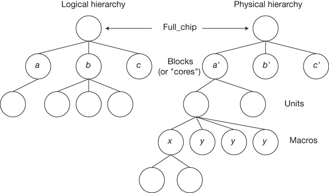
Figure I.3 Logical and physical hierarchical models for an SoC design. Nodes a and a′ are examples of “correspondence points” between the two hierarchies. Physical design reuse is a key productivity goal.
The logical model relates to the optimum functional blocks for sub-chip validation. For full-chip logic simulation, testcase development seeks to exercise block interfaces and interrogate the values of internal register and memory array values. The stability of these control/observe signal definitions in the logic hierarchy is paramount to expediting testcase preparation and maintenance. A relatively shallow logical hierarchy is common, to keep the number of sub-chip validation tasks in check.
Conversely, the physical hierarchy is typically much deeper. Clock and power domains strongly influence the physical definition. In addition, there is a goal to leverage any opportunities for circuit and layout design reuse due to the intensive engineering resources needed for a new custom implementation. As a result, the physical design typically consists of a hierarchy of cells instanced in macros, units, and blocks. (These are common terms for the levels of the physical hierarchy; a microprocessor- or microcontroller-level block is also typically denoted as a core.)
The project team must define the correspondence points between the two hierarchies to ensure that the final chip design is fully consistent. The choice of correspondence points requires an intricate trade-off. Deferring logical-to-physical equivalence checking to the full chip model introduces a significant risk late in the project schedule. Requiring correspondence deep in the hierarchies may be more expeditious but may also impose undue influence on how the logical/physical signal interfaces are defined and maintained. Ideally, the physical implementation should have minimum impact on the definition of logical functionality and vice versa. The typical project decision is to enforce and verify correspondence at the block (or core) level.
As an aside, an increasingly important design flow utilizes synthesis of a logic block to an equivalent model of interconnected basic logic functions from a cell library (see Chapter 7). Each library function has a physical implementation that has been previously qualified. These physical layouts are then automatically placed and interconnect routes generated from the synthesized netlist. This automated flow effectively generates correct logical-to-physical correspondence for the block.
I.2 Managing Inter-Block Glue Logic
Inevitably, logic functionality and physical circuitry reside between the hierarchical blocks. The most common example is the need to insert signal repowering buffers or sequential circuit repeaters between the output of one block and the input to another (see Figure I.4).
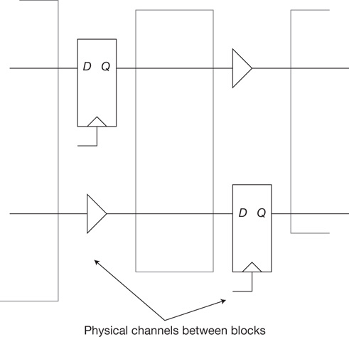
Figure I.4 Functionality present between blocks is typically denoted as “glue logic.” The figure illustrates both signal repowering (buffering) and insertion of a sequential “repeater” for a global signal between blocks.
These circuits prevent poor electrical characteristics on a signal transition due to the effects of a long signal wire or, in the case of a sequential repeater, to maintain synchronous timing between blocks. The cycle latency of a repeated signal is part of the chip functional model and needs to be validated. The physical circuits for the glue logic require allocated chip area between blocks, corresponding signal wiring tracks, and connectivity to power/ground (see Section 8.1 in Chapter 8, “Placement”). Another example of glue logic would be any manufacturing test multiplexing logic to toggle between functional operation and specific test modes for individual blocks.
The full chip methodology is likely to impose restrictions on how these glue functions are represented. It may be suitable (albeit perhaps unwieldy) to simply add these functions to the top of the chip hierarchy as a large collection of flat cell instances; however, these cells will be physically scattered, necessitating electrical analysis with these cells merged with all block abstracts. Alternatively, cells located in a physical channel between blocks could be grouped into a single hierarchical instance in the full chip model and analyzed as just another block. However, this second approach directly ties the physical implementation to the logical model of the chip functionality. As the physical design evolves, the inter-block signals buffered and/or repeated through a specific channel will likely change. With this alternative approach, the input/output pins and internal signal names within these glue blocks will be in flux, disrupting the logical validation testcases that may refer to these (hierarchically qualified) signals.
The most aggressive approach for managing global glue logic cells would be to allow them to be placed and connected within the physical boundary of a design block, perhaps to provide a more optimum buffer/repeater cell location along the length of the global connection. This “channel-less” design methodology is depicted in Figure I.5.
This would require the most intricate methodology for maintaining logical and physical models. Blocks would need to be analyzed, including the electrical and thermal influence of the embedded global circuits, introducing interdependence between block and full-chip design closure in the methodology.

Figure I.5 Physical placement of glue logic within blocks in a “channel-less” design methodology.
As mentioned at the beginning of this overview discussion, no single set of methodology flows and data management policies is best suited to all chip design projects. Cost, resource, and schedule constraints will necessitate trade-off decisions on what project milestones are established. Checkpoints will be defined that gate the integration of individual logical and physical blocks to the full-chip model, with criteria for the sufficiency of block-level functional validation and electrical analysis. This text describes the characteristics of individual flow steps, focusing on the key features and options that are pertinent to the methodology choices to be made.
One additional cautionary note is worth highlighting: As a new chip product proposal is being evaluated for funding and assignment of engineering resources, so must the methodology be incorporated into the review, including related EDA software and IT cost estimates. It is tempting to begin the design activity to meet project schedules, deferring any open methodology issues until nearer the project milestone associated with the issue. However, such a strategy simply shifts the schedule pressure to the methodology team, which must then ensure delivery of EDA tools and flows with the requisite functionality (and testing) on a project-critical deadline. Commencing a design with major open flow requirements will almost assuredly result in project delays and unforeseen resource impacts.
A successful chip project employs a well-defined, documented methodology that has been finalized prior to (or at least during) the project kickoff phase. Ideally, a trial design could be accelerated through block-level flows. This trailblazing design would be representative of the clocking, power delivery, and test micro-architecture prevalent throughout the full chip so that any lacking tool/flow functionality could be identified and promptly addressed. An early collaboration among the methodology team, the chip design lead engineers, the chip project manager(s), the EDA tool/flow support team, and the IT resource management staff on an appropriate methodology will result in more predictable project execution and milestone completion.