
Chapter 1. Introduction
1.1 Definitions
1.1.1 Very-Large-Scale Integration (VLSI)
The amount of functionality that can be integrated on a single chip in current fabrication processes is associated with the term very-large-scale integration (VLSI). Preceding chip design generations were known as small-scale integration (SSI), medium-scale integration (MSI), and large-scale integration (LSI). Actually, VLSI has been used to refer to a succession of several manufacturing process technologies, each providing improved transistor and interconnect dimension scaling. A proposal was made to refer to current designs as ultra-large-scale integration, but the term ULSI has never really gained traction.
The complexity of a new VLSI design project is used to estimate the engineering resources required. However, it is not particularly straightforward to provide a single metric for describing the complexity of a VLSI design and its associated manufacturing technology. The previous fabrication technology generations were predominately dedicated to either digital or analog circuitry. For digital designs, the number of equivalent NAND logic gates was typically applied as the measure of design complexity, and the logic density, measured in gates/mm**2, was the corresponding technology characteristic. The succession of VLSI manufacturing processes has enabled a much richer diversity of digital, analog, and memory functions to be integrated, making a logic gate estimate less applicable to the design and making gates/mm**2 less representative of the process. The embedded memory technologies available from the fabrication process have a major impact on the physical complexity of the chip design, with options for volatile (e.g., SRAM) and non-volatile (e.g., flash) array circuits. For designs with significant on-chip memory requirements, the specific memory cell implementation is a strong factor in estimating the final chip layout area (and, thus, cost). The number of metal interconnect layers available in the VLSI process—especially the electrical resistance and capacitance of each layer—also has a tremendous influence on the engineering resources needed to achieve design targets.
In summary, the complexity of a VLSI design is not easy to define when estimating project difficulty. Comparisons to the resources needed for previous designs are often insightful if a comparable methodology was used. As will be discussed shortly, the ability to reuse existing logical and physical intellectual property is a major consideration when preparing a project plan.
1.1.2 Power, Performance, and Area (PPA)
The high-level objectives for any new design are typically the power, performance, and full-chip area, typically referred to as the “PPA targets.”
The chip power dissipation target is an integral specification for any product market, from the battery life of a mobile application to the electrical delivery (and cooling) for racks of equipment in a data center. The methodology includes a power calculation flow; actually, multiple flows are used to calculate a power dissipation value. Initially, signal switching activity from functional simulation testcases provides a (relative) measure of active power dissipation, using estimates for signal loading. Subsequently, a more detailed measure is calculated using the physical circuit implementation with resistive losses. Multiple modes of chip operation may require power dissipation data as well. For example, a standby/sleep mode requires a calculation of (inactive) transistor leakage currents rather than the active power associated with switching transients.
The performance targets of a design may involve many separate specifications, and analyzing each of them requires methodology flow steps. The most common performance target is the clock frequency (or, inversely, the clock period) applied to the functional logic timing paths between flops receiving a common clock domain signal. Logic path evaluation must complete in the allocated time period. In addition, a myriad of other (internal and external) design performance specifications are covered by the timing analysis flow, including the following:
(Maximum) clock distribution arrival skew between different flops
(Minimum) test logic clock frequency for the application of test patterns
Chip output signal timing constraints, relative to either an internally sourced clock sent with the data or an applied external clock reference
The area of the chip design is a factor in determining the final product cost. The larger the area, the fewer die sites available on the fabricated silicon wafer. A larger die likely requires a more expensive chip package, as well. The manufacturing production yield is strongly dependent upon the die area due to the probabilistic nature of an (irreparable) defect present on a die site. The accuracy of the chip area estimate prepared as part of the initial project proposal is crucial to achieving production cost targets. The methodology does not have a direct influence on this estimate, perhaps, but it may still play an important role. As mentioned earlier, a trial block design exercise may be useful to test the flow steps and provide data for representative block area estimates. It will also provide insights into the number and type of interconnect layers needed to complete block signal routes and achieve performance targets. The specific metallization stack selected for the block and global signal routes will impact fabrication costs, with each metal layer providing particular signal delay characteristics and signal route capacity (measured in wiring tracks-per-micron on the preferred route direction for the layer).
1.1.3 Application-Specific Integrated Circuits (ASICs)
Electronic products were traditionally designed with commodity part numbers, using SSI, MSI, LSI, microprocessor, memory, and analog (including radio-frequency) packages on printed circuit boards (PCBs). Unique fabrication process technologies were introduced to add commodity programmable logic and programmable (non-volatile) memory parts to provide greater product differentiation. With the transition to VLSI chip designs and processes, a number of factors led to the development of entirely new design methodologies:
The markets for electronic products grew tremendously and became much more diverse. Mobile products required intense focus on reducing power dissipation. Product enclosures pursued unique form factors, minimizing the overall volume. Both trends necessitated maximizing the integration of digital, memory, and analog functions. (Packaging technologies were also driven toward much higher pin counts and areal pin densities for PCB attach.)
Product differentiation became increasingly important to capture market share from competitors.
The advances in EDA tool algorithms were being transferred from academia and corporate research labs to the broader microelectronics industry, providing vastly improved productivity for designers to represent and validate functionality and implement and analyze the physical layout. Hardware description language semantics were introduced to allow functionality to be described at a much higher level of abstraction than the Boolean logic gate schematics used for MSI/LSI designs. For physical design, algorithms for automated circuit placement and signal routing were introduced. The circuits to be placed were selected from a previously released cell library, whose individual layouts had been verified to their logical equivalent and whose circuit delays had been characterized. The complexity of these library elements typically covered a wide range of SSI and MSI logic functions, small memory arrays and register files, input receiver and output driver pad circuits, and (potentially) simple analog blocks (e.g., phased-lock loop, ADC/DAC data converters).
These factors led to the adoption of a new set of products known as application-specific integrated circuits (ASICs).
A number of companies began to offer a full suite of ASIC services, such as developing cell libraries, releasing EDA tool software suites, assisting with PPA estimation, performing cell placement and routing, generating test patterns, releasing product data to manufacturing, executing package assembly and final test, and completing product qualification. Design teams were to follow the ASIC company’s documented methodology. The handoff from design to services consisted of the final logical description, including a netlist of interconnected cells plus performance targets. The detailed netlist was synthesized from the hardware description language functional model, either manually or with the aid of logic synthesis algorithms. In return, the ASIC company provided an upfront services and production cost quote for completing the physical implementation and release to manufacturing, simplifying the budgetary planning overall.
There were still many integrated circuits (ICs) developed using a full custom methodology, where all functional blocks consisted of unique logic circuits and manually drawn physical layouts, without utilizing automated placement and routing of library cells. This custom methodology was used only for high-volume parts, where the intensive engineering resources required could be amortized over the sales volume. (As ASIC designs typically were between commodity LSI parts and custom VLSI designs in terms of complexity, with functionality implemented using an existing cell library, these designs were also referred to as semi-custom.)
1.1.4 System-on-a-Chip (SoC)
As VLSI process technologies continued to evolve, offering increasingly scaled transistor and interconnect dimensions, there were several shifts in the ASIC market:
The complexity of physical library content required to meet application requirements grew—for example, larger and more diverse memory types (caches, tertiary arrays); programmable fuse arrays; high-speed external serial interfaces with serializer/deserializer (SerDes) physical units; and, especially, larger functional blocks (microcontrollers and processor cores for industry standard architectures).
Design teams were seeking multiple, competitive sources of these new library requirements. Rather than relying solely on the library available from the ASIC services provider, design teams sought sourcing of IP from other suppliers. This initiative was either out of financial interests (specifically, lower licensing costs) or technical necessity (e.g., if the ASIC provider did not offer a suitable PPA solution for the IP required).
Design teams sought to be more directly involved in the selection of the silicon fabrication and package assembly/test suppliers. Much as with the negotiations with IP suppliers for library features, design teams were willing to invest additional internal resources to investigate and select production sources. The goal was to more closely manage operational costs and balance supply/demand order forecasts rather than to work through the ASIC services company interface.
EDA software tools began to be marketed independently from the ASIC services company, allowing design teams to develop their own internal methodologies. The breadth of responsibilities for the internal EDA tool support team grew. The design engineers providing (part-time) EDA software support for the ASIC design methodology were consolidated into a single “CAD department.” This new and larger organization was established with the mission to provide comprehensive EDA software support for the internal methodology to all design teams. Comparable tools from different EDA vendors were subjected to benchmark evaluations to ensure suitability with the proposed methodology, confirm PPA results on representative blocks, and measure the tool runtime and IT resources required. These benchmarks also helped the CAD team assess the task of developing flow scripts and utilities around the tool to integrate into the methodology. Software licensing costs from the EDA tool vendor were also a major factor in the final competitive benchmark recommendations.
These shifts in the ASIC market resulted in the growth of several new semiconductor businesses and organizations:
Semiconductor foundries—These companies offer silicon fabrication support to customers submitting designs that have been verified using their process design kit (PDK) of manufacturing layout design rules and transistor/interconnect electrical models.
Outsourced assembly and test vendors (OSATs)—These specialty companies provide a broad set of services, including good die separation from the silicon wafer, die-to-package assembly, and final product test/qualification.
EDA tool vendors—The EDA vendors vary in terms of their software tool offerings. Some focus on point tool applications for a specific methodology flow step. The larger firms have worked to integrate multiple tools into an integrated platform, encompassing multiple flow steps.
Industry standards organizations—To facilitate the use of EDA tools from multiple suppliers in a design methodology, a set of industry-standard data formats were developed for tool input/output at various common step interfaces. For high-impact flow steps, the Institute of Electrical and Electronics Engineers (IEEE) has taken ownership of these evolving standards. For example, the syntax and semantics of the hardware description languages Verilog (and its successor, SystemVerilog) and the VHSIC Hardware Description Language (VHDL) are IEEE standards, subject to periodic updates. The format for representing the electrical characteristics of signal interconnects extracted from a physical circuit layout is the Standard Parasitic Exchange Format (SPEF), another IEEE standard. Other data format standards are maintained by industry consortia, with approval committees comprised of member company representatives. The Open Artwork System Interchange Standard (OASIS) definition for the file-based representation of physical layout data is maintained by the Semiconductor Equipment and Materials International (SEMI) organization.
De facto standards—There are some de facto data representation standards that are not formally approved and maintained. Their use became so widespread, often because of market-leading tools, that most EDA vendors support the adoption of the format to prevent their own products from being at a disadvantage to integrate into a flow step. The Simulation Program with Integrated Circuit Emphasis (SPICE) circuit simulation program reads in a netlist of interconnected transistor models and electrical primitives. After the transient circuit simulation completes, the signal waveform results are written. Both the SPICE netlist and output waveform file formats are de facto standards. The predecessor format to OASIS for layout description, the Graphic Database System (GDS)—along with its long-used successor, GDS-II—is another de facto standard. The Fast Signal Database (FSDB) format is a de facto standard for representing functional logic simulation results.
When evaluating a tool to integrate in the methodology flow, specific attention must be given to the consistency of the input and output file formats between steps. Data translation utilities added into a flow introduce the risk of data integrity loss if the utility does not recognize—or, worse, misinterprets—a data file record. This is especially important for de facto data formats. (It is also crucial to examine an EDA vendor’s tool errata documentation for any semantics included in a standard specification that are not fully supported to determine the potential impact to the design team.)
Intellectual property suppliers—The ASIC shift is perhaps best illustrated by the importance of companies that have focused on the development of complex intellectual property licensed to design companies for integration. Design teams (and/or their ASIC services provider) may not have the expertise or financial and schedule resources to develop all the diverse functionality required for an upcoming project. A separate IP vendor, often working in close collaboration with the foundries during initial development of a new process technology, could fabricate and qualify a large IP block. The emergence of standard (external) bus interface definitions (e.g., DDRx, PCIe, USB, InfiniBand) has accelerated this IP adoption method. Design teams need not be experts in the functional and electrical details of these protocols but can leverage the availability of existing IP for reuse. (Note that this discussion refers to IP functions that include a physical implementation, in a specific foundry’s process technology; there are also functional model-only IP offerings, described shortly.)
Several EDA vendors have also recently expanded their product offerings to include IP libraries. There is a natural synergy between advanced EDA tool development and IP design for a new fabrication process. The EDA team collaborates with the foundry during process development to identify new tool features that are required. The IP team also has an early collaboration with the foundry to prepare designs for fabrication and testing so that the IP is available for leading customers when the process qualification is complete. As part of the EDA vendor engineering staff, the IP team also helps test and qualify the new software (with software licenses for free, to be sure). This synergistic relationship between tool and IP development is proving to be financially successful for the EDA vendor and also to improve the quality of new EDA software version releases.
For similar reasons, the foundries are also increasingly offering IP libraries. The foundries have internal process development teams focused on specific circuit requirements (e.g., device characterization and reliability, memory bit cell technology, fuse programmability). As with the EDA vendors, the foundries are also investing in enhancing internal circuit design expertise. It is a natural extension of these process development areas for the foundry to offer customers IP libraries consisting of diverse sets of functionality, including a base cell library, I/O pad circuits, memory (and fuse) arrays, and so on. The foundry may offer the IP library at an aggressive licensing price as a means of attracting more customer “design wins” to secure the corresponding manufacturing volume and revenue.
In summary, VLSI designs have evolved in complexity from the earlier ASIC approach, both in terms of the diversity of integrated IP and the unique methodologies applied by the design team. A description that better describes the current class of VLSI designs is system-on-a-chip (SoC).
1.2 Intellectual Property (IP) Models
SoC chip designs incorporate a range of physical IP components of varying functional and PPA complexities.
1.2.1 Standard Cells
Basic logic functions are collected into a library of physical layout cells with corresponding electrical models. Design blocks are implemented by the placement and routing of these cells to match the description of a logical netlist. The layout of these standard cells adheres to a template applied throughout the cell library. Specifically, the template defines:
The position and width of (lower-level) metal layer power and ground rails
The number of lower-level metal wiring tracks available for signal connections within the cell implementation
Valid locations for pins to connect to the cells with signal routes
The cell layouts are thus constrained in one dimension (e.g., the vertical dimension in Figure 1.1) and typically span a variable width in the other dimension to complete the layout connections. In Figure 1.1, note that the standard cell template employs a shared power and ground rail design. The orientation of alternating rows of cells would be flipped in the vertical direction to share rail connections with the adjacent row. The width of the rails in the template would be designed to provide a low-resistive voltage drop for the current provided to both adjacent cell rows.
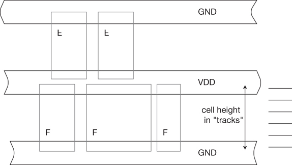
Figure 1.1 Standard cell layout template example, illustrating shared power and ground rails. Logic cell layouts are one (perhaps two) template rows tall and of variable width. The template cell height spans an integral number of horizontal wiring tracks.
The standard cell library content is thus limited to the logic functions that can be successfully connected within the wiring track limit. Typically, flip-flop circuits are the most difficult to complete; their layouts often define the allocation of intra-cell tracks in the template.
Given the wiring track constraint, some cell layouts may add connections on an upper metal layer, which is typically used for inter-cell routes. In these cases, the placement and routing methodology needs to accept a partial route blockage map, honoring the unavailability of these tracks for signal routes due to the cell layouts. Some libraries may also include “two-high” cells, under the assumption that the placement flow can accommodate both one-high and two-high dimensions; this enables a richer set of library logic cells to be available.
Cell Drive Strengths
To assist with PPA optimization during physical implementation, each logic function in the standard cell library is likely to be offered in multiple drive strengths. For example, a function built with minimum-sized transistors may be denoted as 1X. Increasing transistor sizes may enable 2X, 4X, and so on alternatives, as illustrated in Figure 1.2. The template height constraint limits the transistor dimensions in the physical layout; larger drive strength variants need multiple transistor fingers connected in parallel, spanning a greater cell width. (A transistor finger is an individual device with common drain, source, gate, and substrate connections to the other fingers connected in parallel. The total device width is the sum of the individual finger widths. Section 10.2 discusses layout proximity effects, where the surrounding layout topology impacts the device performance. In this case, the device current model for the individual fingers varies, necessitating expansion of the total device width into the individual fingers for detailed circuit analysis.)
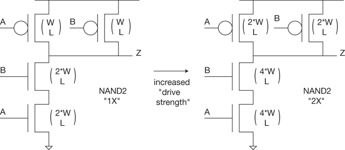
Figure 1.2 Cell library functions are provided in multiple drive strengths. The wider devices used for higher drive strengths may require a layout using parallel fingers. The pin input capacitance is the sum of all device input capacitances, each of which is proportional to the product of device width and length.
The cell layouts must all observe a minimum half-rule space within the template boundary to allow adjacent cell placements to satisfy the process lithography requirements. Although the output impedance of a higher-drive-strength cell is reduced, providing improved signal transition delays, the capacitive loading presented to the circuits sourcing the input pins is increased, adversely impacting their performance and power dissipation. Performance optimization requires an incremental path-oriented algorithm for cell drive strength selection to evaluate the relative trade-offs between improved drive strength and increased loading for cells and interconnects in the path.
Cell Threshold Voltage Variants
Another cell library option is to offer the logic functions with circuit variants using different transistor threshold voltages available in the fabrication process technology. For example, a single drive strength of a cell could be available using standard Vt (SVT), high Vt (HVT), and low Vt (LVT) transistors. The lithographic layout rules from the foundry typically facilitate placing SVT, LVT, and HVT transistors in close proximity; that is, SVT, LVT, and HVT cells could be placed adjacent to each other. (In the most advanced process nodes, there are new lithographic rules impacting the adjacency of different device threshold types, necessitating additional spacing between cell threshold variants.)
The circuit transition delay for an LVT cell is improved over its SVT equivalent, without the cell area and input capacitive loading increase associated with a higher-drive-strength version. The trade-off is that the LVT cell static leakage current power dissipation is greatly increased. Whereas a 2X drive strength transistor size effectively doubles the leakage current over 1X, the leakage current for an SVT-to-LVT cell exchange increases exponentially. (If a circuit timing delay path is far less than the allocated clock period, the positive timing slack could be applied to the substitution of HVT cells for SVT equivalents, reducing leakage power substantially.) A visual representation of this trade-off is provided by the Ion-versus-Ioff curve from the foundry shown in Figure 1.3, which illustrates the process target for transistor on-current drive strength (in saturation mode) versus the off-leakage current, for a reference transistor size.

Figure 1.3 Example of an Ion-versus-Ioff curve from the foundry, illustrating the process target for device currents with different Vt threshold voltages (in saturation mode, for a reference device size). The curve allows a (rough) comparison between processes. The “device current gain at constant leakage power” is depicted for two process targets (with scaled reference device sizes).
Note that the graph axes in Figure 1.3 are log-linear, highlighting the exponential dependence of Ioff on transistor Vt. The line connecting the LVT, SVT, and HVT points is artificial; it simply illustrates the linear Ion and exponential Ioff dependence on Vt. There are no transistor design offerings along the curve; they are strictly at the different Vt fabrication options. Nevertheless, the curve is extremely informative, in case the foundry and its customers opt to evaluate an investment in another transistor Vt offering for specific PPA requirements (e.g., extra high Vt [EHVT]). Such a curve is also often used to compare successive process generations. The horizontal distance between the curves for two processes is a benchmark for performance improvement at constant leakage power (for the reference size transistor in the two processes). The vertical distance estimates the leakage power improvement at constant performance. It should be highlighted that these are transistor-specific data points; to realize these gains between processes, there are also scaling assumptions on interconnect lengths, interconnect R*C parasitics, and power supply values that need to be evaluated. The selection of the optimum combination of drive strengths and Vt offerings for millions of cells in a netlist for PPA optimization is perhaps the most complex set of EDA tool algorithms.
1.2.2 General-Purpose I/Os (GPIOs)
The base cell library also includes input pad receivers and output pad drivers (not integrated into a specific physical IP interface block). These general-purpose input/output (GPIO) cells have numerous variants with different characteristics, such as:
Vin and Vout logic threshold levels (Vout measured with a specific DC load current)
Output driver impedance, for matching to the package impedance to minimize transmission line reflections
Bidirectional driver/receiver circuits (with high-impedance driver enable control), in addition to unidirectional drivers
Receivers with hysteresis feedback to improve noise immunity
Electrostatic discharge (ESD) protection (see Section 16.3)
The I/O cells have their own layout template, which is much larger than the standard cell template. These circuits incorporate very-high-output drive strengths with many parallel transistor fingers and much larger power/ground rails to deliver greater currents at low voltage drop. In addition, the voltage levels connected to these GPIO circuits are typically distinct from the internal IP voltages. For example, external interface voltages may be in the range of 1.2 to 1.8V, while the internal circuitry for current process nodes operates below 1V. The GPIO circuits may also use a different set of thick gate oxide dielectric field-effect transistors to support exposure to higher voltages, with additional layout constraints. Although some methodologies support the placement of GPIO cells scattered throughout the die area, the majority of methodologies allocate the GPIO templates (and related I/O power/ground rails) strictly to the die perimeter.
1.2.3 Macro-cells
The elementary logic circuits in the standard cell library are the components for the physical implementation of larger functional designs. However, additional productivity in generating the logic netlist could be achieved if more complex logic cells were available. A larger set of PPA optimizations would likely be enabled as well. For example, an n-bit register consisting of n flops sharing a common clock is a typical complex logical design element in a library. An n-bit multiplexer sharing common select signal(s) is also common. An n-bit adder is another, with a performance dependence on the specific adder implementation. In all these cases, there is a goal to minimize the delay of a critical timing path by reducing the loading on a high fan-out input connection or optimizing internal (multi-stage) logic circuit delays.
Two types of offerings have been added to cell libraries for these more complex macro-cells: a custom physical implementation and a logic-only representation. As mentioned earlier, physical design methodologies are often required to support larger cell dimensions than a one-high template row standard cell layout. Macro layouts can be added to the library if the methodology supports more varied physical cell dimensions. Within the layout, special focus would be given to ensuring low skew of high fan-out inputs and short delays for critical paths within the macro. (There is also the decision of whether the macro layout would be given the flexibility to discard the template power/ground rail definitions from the standard cell library and employ a unique rail design, with continuity only present at the macro edges for abutted cells.) However, offering these additional custom physical layout components would add to the task of library timing model characterization and electrical analysis.
An alternative would be to add a level of hierarchy to the cell library; in this case, a logical macro would be defined, and it would consist of a specific netlist of base standard cells to implement the function. Figure 1.4 depicts an example of an n-bit multiplexor, consisting of a hierarchy of n single-bit mux cells. Buffer cells could also be judiciously added to the netlist for high fan-out internal signals and, potentially, macro outputs.

Figure 1.4 A logical macro defines a complex function composed of existing standard cells. An n-bit 2:1 multiplexor is depicted. Critical signals within the macro definition would receive specific buffering. Relative cell placements optimize the routing track demand and interconnect loading within the macro.
The unique feature of the logical macro would be the inclusion of relative placement directives with the library model. The placement flow would encounter the logical macro in the netlist, expand to its primitive cell netlist, and apply the relative placement description to treat the constituent cells as a single component that would be moved in unison during placement optimization.
There are several advantages of using logical macros, including the following:
No additional characterization and electrical analysis of the power and timing delays of a complex function are required. The final netlist of expanded (characterized) cell primitives is used.
Subsequent cell-based optimizations are available. Once the logical macro is part of the physical implementation, cell-based power and performance optimizations are applied, such as the substitution of HVT cells to save leakage power. The drive strength of macro output cells could be optimized for the actual loading in the specific context of the larger physical block layout. (The cell dimensions could vary during optimization; the placement algorithm would resolve any cell overlaps while maintaining the relative positioning.)
The relative cell placement should (ideally) guide the router to short connections for critical signals. With alignment of cell pin locations resulting from the relative placement, simple and direct route segments are likely. The risk of a circuitous connection on a critical macro signal can be further reduced by utilizing router features that accept a signal priority and/or preferred route layer setting for specific signals; these router directives could also be added to the logical macro library model.
Layout engineering resources required for library development are reduced. It is typically much easier to develop and verify the logical macro (and relative placement and router directives) than to prepare a custom circuit schematic and layout for the function.
The primary disadvantage of the logical macro approach is that the resulting implementation typically has less optimal PPA characteristics than a custom design. Whereas there is a clear granularity in logic cell drive strengths in the library (e.g., 1X, 2X, 4X), a custom schematic design could utilize greater variability, tuning the drive strength optimally for the loading within the custom macro layout. Also, due to the discrete size of the template in terms of wiring tracks, individual cell layouts may not fully utilize the area of a single-row 1xN (or double-row 2xN) template. A custom layout would likely be more area efficient.
These are complex trade-offs that need to be made by the library development team. The decisions on these trade-offs also have a strong interdependence with the features of the physical flows in the design methodology.
1.2.4 Hard, Soft, and Firm IP Cores
The evolution of SoC design integration has been enabled by the availability of complex IP functions that design teams can quickly integrate. The most prevalent examples are large memory arrays; analog blocks for high-speed external signal interfaces; and (especially) microprocessor, microcontroller, and digital signal processing cores. More recent complex IP examples include cryptographic units, graphics/image processing units (GPUs), and on-chip bus arbitration logic for managing communication between cores, potentially using advanced network communication protocols. (The IP core is also commonly referred to as a specific application “unit,” as in GPU or CPU.)
These IP designs are typically not developed by the design team but are licensed from external suppliers, each of which offers expertise in a specific microprocessor architecture or high-speed interface design standard.
Complex IP may be provided in different formats that have been given a unique terminology. The following sections discuss the various terms.
Hard IP
A hard IP offering is a large, custom physical layout implemented and qualified in a specific foundry technology. The IP vendor has developed the implementation to its own PPA targets, which hopefully align with customer requirements. The IP layout typically fully utilizes internal signal interconnect routes on several metal layers—more than for the standard cell library and macros. The IP vendor has also made an assumption on the appropriate metallization stack choices for the entire SoC, up to the top metal layer used in the hard IP layout. The physical integration of this layout in an SoC design involves providing global power distribution and signal routing to the layout pins (on the corresponding pin metal layers and route wire widths) that satisfy the vendor’s specifications.
The vendor provides a functional model(s) for the IP to use in SoC validation. For microprocessor or microcontroller core IP, a software development kit (SDK) is included for the generation of system firmware. Functional simulation testbench suites may also be provided to the SoC team to assist with validation of the processor bus arbitration logic with other units. The IP vendor will also have implemented a specific manufacturing test strategy for the core. A special test mode may be defined to allow the core to be functionally isolated from the remainder of the SoC, to enable the vendor’s test patterns to be applied and responses observed. Indeed, an industry-standard core wrap architecture has been developed to support isolating a core in an SoC for production testing.[1,2]
The hard IP release provides the vendor with the greatest degree of protection of proprietary information. (Although license agreements include strict policies on unauthorized disclosure of the vendor’s model data, IP leaks are nevertheless a major concern for the vendor.) A special feature that has been incorporated in EDA vendor functional simulation tools is the capability to link a binary executable when building the full SoC model. The IP vendor may thus provide the hard IP simulation model as a compiled executable rather than as a source logical description. A unique programming interface standard has been defined by EDA tool and IP vendors. This code is added to the model to allow the IP vendor to limit access within the simulation environment to selected micro-architectural signal values for query and debug.[3,4]
The main disadvantages of the hard IP release are the direct ties to a specific foundry process and metallization stack (which must be consistent with all the IP on the SoC, of course) and the lack of configurability of micro-architectural features. The other forms of IP release offer greater flexibility in IP core features and production sourcing, with a corresponding reduction in IP vendor information protection.
Memory arrays and register files for SoC integration are a special case of hard IP. The diversity in required array sizes is great, as are specific features that may be desired, such as partial write (read/modify/write). Register files vary widely in size, as do the number of uniquely addressable (and simultaneously accessible) read/write ports. It would not be feasible to release a specific hard IP design for each unique application, nor would it be attractive to SoC design teams to be required to adapt their architectures to a very limited set of array and register file offerings. However, these functions require an aggressive layout style, as their PPA is typically critical to the overall SoC design goals.
IP vendors have addressed these customer requirements by offering array generators. Customers provide array configuration parameters as inputs to the generator. The output is equivalent to a hard IP release—that is, a physical layout (ideally, close to the density of a full custom layout); a functional simulation model; timing models for clock/address/data read-write access operations; and a production test model. The generator infrastructure allows the IP vendor to more easily support multiple foundries for customers. The foundry may offer different, proprietary high-performance or high-density array bit cell designs for use in the generators, enabling a wider range of PPA support.
There are some minor considerations when incorporating an array or a register file generator into the design methodology:
The range of sizes supported by the generator must fit the SoC architecture.
The timing model calculator within the generator must fit the operating temperature and supply voltage ranges of the target SoC application.
The test model from the array generator must fit the overall SoC test architecture for applied patterns and response observability. Specifically, large register files present a trade-off in terms of whether the test model represents an addressable array or expands to individual register bits, with the corresponding test architecture for each bit as a flip-flop.
Soft IP
A soft IP release is strictly a functional model, without a corresponding physical implementation. The model is typically provided using the semantics of a hardware description language (HDL). The common HDLs, SystemVerilog and VHDL, both readily support passing configuration parameters down through the logical model hierarchy, offering considerable flexibility in micro-architecture exploration before finalizing the functional design.
The physical implementation is realized through the synthesis of the HDL model to a target standard cell plus macro library (and the mapping of arrays to a generator). EDA tool vendors provide logic synthesis tools to compile the HDL model and subsequently implement the function as a netlist of cell library components, optimizing to PPA constraints.
The use of soft IP provides an easy path to evaluating multiple foundries, using different libraries when re-exercising logic synthesis and physical design flows. Similarly, it allows for rapid experimentation with different PPA targets. The primary design disadvantage is the larger area and reduced performance compared to a hard IP implementation.
Firm IP
A less common format is for the IP vendor to provide a cell-level netlist rather than an HDL model. The netlist may be in terms of instances of a cell library targeting a specific foundry or consisting of generic Boolean logic primitives. The latter would allow for multiple foundry evaluation by a straightforward, but perhaps suboptimal, synthesis mapping of Boolean primitives to different cell libraries.
This firm IP release resembles the logical macro methodology. The cell-based implementation would enable drive strength and power optimizations during physical design, from the “manually synthesized” firm IP netlist. Some limited configurability may be offered by the vendor providing the firm IP, adapting the output cell netlist to customer input parameters. With the ongoing improvements in logic synthesis algorithms and the increased experience with synthesis in SoC design teams, the release of firm IP formats by vendors has declined in favor of releasing soft IP HDL models.
The soft IP and firm IP approaches provide greater design flexibility in micro-architecture and foundry sourcing. In return, the IP vendor relinquishes some degree of information protection.
1.2.5 “Backfill Cells”
A special class of cells are included in the library and are crucial to all block implementations. These cells are added to complete the physical layout without a corresponding instance in the netlist.
The cell template dimension is typically chosen to enable intra-cell signal connections to be completed on the most complex circuits, on the allocated metal layers for cell layouts. The access points to the cells for inter-cell routing are associated with pin shapes in the cell layout, placed to align with wiring tracks on upper-level metals. The metallization stack utilizes thicker metals for improved electrical characteristics on upper layers, with corresponding increases in the (minimum) wire width and space; thus, the wiring track density is reduced for these layers. In addition, the cell library may include high fan-in logic primitives for efficiency in the total logic gate path length to realize a timing-critical function. For example, wide AND*OR cells are useful in many datapath-centric designs (e.g., a 2-2-2-2 AND*OR with each AND gate receiving a data and select input). Placement of these cell layouts with high fan-in is likely to introduce a high local pin density. The reduced number of available tracks on the inter-cell routing layers combined with a high local pin density may result in routing congestion when attempting to complete the block physical design. The routing tool may be unable to find suitable (horizontal and vertical) segments for all the netlist connections, resulting in incomplete signals (known as overflows).
The physical block layout area allocated to route the complete netlist may thus need to be enlarged. Cell area utilization substantially less than 100% is used to gain confidence in achieving a fully routed solution. The library vendor provides utilization guidelines, based on previous experimentation; for example, a recommendation of ~80% utilization is common. (Placement algorithms evaluate local pin density during cell positioning and space cells apart to reduce route congestion.) The net result is a significant vacant area within the block layout, both within and around the perimeter of the block boundary.
The library contains backfill cells (of varying widths) to insert into vacant locations in the block. These completion cells can be quite varied in content and purpose:
Dummy cells for photolithographic uniformity—The backfill cell may add dummy transistors to maintain a more uniform grid of transistors between functional cells to reduce the variability in lithographic patterning of the critical dimension transistor gate length.
Local decoupling capacitance—Expanding upon the addition of non-functional transistors in vacant cells, a relatively simple connection of devices provides a capacitance between the VDD supply and GND rails (see Figure 1.5). These decap cells can be easily inserted in the unoccupied cell locations after routing and prior to electrical analysis.[5]
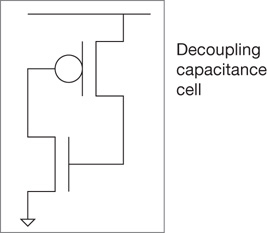
Figure 1.5 Schematic for the “cross-coupled devices” decoupling capacitance cell, inserted in vacant cell locations. Both devices are operating in linear mode, with maximum Cgate-channel.
The switching activity of logic cells draws supply current. Local decoupling can efficiently provide charge to this transient, minimizing the resistive I*R voltage drop along the rails and without the delayed inductive response through package pins. Indeed, a key facet of the power distribution network (PDN) analysis flow step is to calculate the total dynamic switching transients, the local (inherent circuit and explicit decoupling) capacitance, and the PDN electrical response characteristics to ensure rail voltage transients are within design margins (see Section 14.3).
Gate Array Logic ECO Cells
After an SoC design is submitted for initial fabrication, it may become evident that a logic design modification is required. A change in product requirements may arise while awaiting the first-pass prototypes from the foundry and OSAT. Or, more likely, a bug in the functional design may have been discovered during the ongoing system model validation, after release of the design to the foundry. In either case, there is a requirement to apply an engineering change order (ECO) to the (first-pass) netlist.
The simplest approach would be to simply remove any erroneous standard cells (and their routes) from the physical layout, insert the standard cells to fix the bug, and reroute the updated netlist connections. Indeed, physical design tools commonly have an incremental mode, which accepts a unique netlist syntax for cell instance adds/deletes. The goal of this ECO methodology is to leave the existing physical design as unperturbed as possible to minimize new issues arising during electrical analysis. However, adding and deleting standard cells for a second-pass design implies that all lithography layers for the SoC will likely have been edited, starting with transistor fabrication. The cost of a full set of new lithographic masks will be considerable, and the schedule impact of the full fabrication cycle time will be maximum before updated packaged parts are available.
An alternative approach is to backfill some percentage of the vacant block area with uncommitted transistors. A specific ECO logic function would be realized by adding local metal segments between transistors, vias, and pin locations. An array of transistors could be personalized to a logic function, using only metal and via physical layout edits.
The collection of individual logic functions implemented by the metal personalization of uncommitted transistors is known as the gate array library. An IP library provider may include gate array cells with the standard cell release. Typically, the gate array offering will be a small subset of the standard library, with limited drive strengths and transistor Vt variants available. The ECO design with gate array logic inserted (and, likely, signal buffers added) will not be optimized to PPA design targets. There is certainly a risk that the gate array backfill cells will not be able to implement a set of logic ECO changes, due to limited availability, location, or the impact on overall performance that no longer meets design specifications.
If a gate array library is available, the ECO methodology needs to ensure that all flow steps are consistent with incremental design at the cell netlist level (see Chapter 17, “ECOs”):
Placement and routing tools must accept the incremental netlist syntax and restrict additions to unpersonalized gate array locations.
The full-chip SoC data model used for test pattern generation must reflect the incremental updates.
The extraction of signal interconnect parasitics for electrical analysis must (ideally) also be able to recognize the incremental inter-cell route segments and efficiently update the parasitic network.
A complete logical-to-physical equivalence ECO flow step is required; a netlist update applied directly to the physical layout also needs to be reflected in the HDL source model for functional validation. Designers make functional changes to the HDL model related to the ECO netlist adds and deletes and recompile the HDL for functional simulation. The ECO methodology flow needs to verify the logical equivalence of the updated cell netlist to the revised HDL.
The data version management policies adopted by the methodology need to apply a nomenclature that maintains the evolution of the first-pass design and any succession of ECO netlists. When first-pass prototypes are received from the foundry, hardware system bring-up and debug will be referenced to the original release data while ongoing updates for a subsequent fabrication pass are being developed.
Standard Cell Logic ECO Backfill
A couple of methodology considerations regarding backfill in preparation for subsequent ECOs are worth specific mention. If a gate array cell library is not available, an alternative methodology would be to add a small quantity of standard cells throughout the vacant block area. The inputs to the standard cell would initially be routed to a power or ground rail to tie all inputs to a fixed logic value. Unlike the flexibility of the gate array logic function provided by the personalization of uncommitted transistors, a spare standard cell implies a specific logic function available at that location. The number and diversity of spare standard cells added to the block is a judgment choice. There is a risk that an ECO netlist change may not be efficiently realizable with metal-only lithography updates if the spare logic standard cells are limited in location and function.
Another methodology decision pertains to whether spare flip-flop cells would be inserted to support an ECO that adds a sequential state signal. The gate array backfill library offering may not include flip-flop cells; the connections between transistors to implement a flip-flop are the most difficult within the standard cell template and may not be viable for the uncommitted transistor array. Alternatively, flip-flops from the standard cell library could be selected for insertion and judiciously placed in vacant areas.
The more difficult decision pertains to what consideration should be given to the clock input(s) to the spare flops. During physical design, an effort is made to provide clock signal buffering and load balancing to minimize the arrival skew at the clock signal fan-out endpoints—namely flip-flop inputs and clock gating cells. If spare flops are provided, the ECO routing updates to add the clock connection to the flop will perturb the existing balanced skew; previously valid timing paths (unrelated to the logic ECO modification) may now fail due to increased clock arrival skew. To avoid the issue, the spare flop clock inputs could be part of the original physical optimization, so their subsequent use would not adversely impact the clock timing. However, in this case, spare flops that remain unused result in wasted power dissipation due to the additional clock loading. And, for logical-to-physical equivalence verification, these visible spare flop cells would need to be added to the logical model for the block despite having no functional contribution. A potential requirement to include spare flops in the test model for the original design also needs to be assessed. If the test architecture includes unique test mode clocking, the spare flop may need to be included in the functional description.
The methodology approach selected to optimize the cost/schedule impact of ECO updates requires several trade-off assessments with regard to the specific spare cell library chosen, the number and placement of spare cell logic functions, the number of mask layout layers impacted to implement the ECO, and, for the insertion of spare flops, the impact on the (functional and test) clock distribution.
1.2.6 Cell Views and Abstracts
The cell library release includes numerous views for each element for different methodology flow steps:
Functional model for netlist-level validation—Example flows are logic simulation and logical-to-physical equivalency.
Test model—A description of the prevalent circuit-level manufacturing faults is needed to investigate with manufacturing test patterns.
Timing model—The timing model includes cell pin-to-pin delay arcs, with delays represented as a function of supply voltage, temperature, input pin signal slew, output pin loading, and (potentially) conditional arcs based upon the logic values at other input pins; sequential functions have additional timing data, such as clock-to-data setup and hold constraints. Recent timing models also include detailed data on the output pin transient current waveforms for more accurate signal interconnect propagation.
Physical model—A representation of the physical cell layout, used for placement and routing, includes cell size, route blockages, and pin shapes (including either “connect to” or “full cover” route constraints for the large area pins).
Power model—The power model includes the static leakage power and internal power dissipation for arc transitions, with comparable coverage of voltage, temperature, and signal transitions as the timing model.
Electrical and thermal models—A collection of data derived from the physical layout is used for other flows (e.g., pin capacitance, input pin noise pulse rejection, output pin impedance, power and ground rail currents for signal transitions, self-heating thermal energy).
These views are developed by library generation methodologies to provide model abstracts that are most efficient for the cell-based flows. Library model generation is also commonly referred to as characterization (see Section 10.2). EDA vendors have utilized unique abstract data best suited to their tools. The vendors have collaborated with IP providers to prepare these specific formats as part of library generation methods. Due to the critical importance of these models for all tools and SoC methodologies and the costs associated with library generation, the IC industry is increasingly pushing for (de facto) standards for model view abstract data. Several EDA vendors have responded to this trend by releasing their formats into the open source community.[6] Nevertheless, methodology development requires coordination between specific tool requirements and the cell abstracts released by the IP library supplier.
The automated logic synthesis of a cell-based netlist from an HDL functional description employs optimization algorithms that use data from multiple views for initial logic mapping and subsequent PPA optimizations. There are assumptions inherent to these tool optimizations about the relative ordering of the drive strength and Vt cell variants of each logic function in the library release. For example, when seeking to reduce path delay during timing optimization, the algorithms seek to deploy the “next higher” performance entry for the mapped logic function. The methodology team and IP library supplier should review the criteria used to determine the ordering for cell variants of a logic function to ensure that these criteria are consistent with the SoC design goals. If a design is extremely constrained by static leakage power, the relative choice of LVT cell variants could be reduced (or excluded altogether, with a separate “don’t use” directive to the synthesis flow).
1.2.7 Model Constraints and Properties
In addition to the abstract data that describe the cell to the EDA tools, there is a view for some cells that reflect any restrictions on the cell usage in the context of the full netlist. The cell design may have incorporated specific assumptions about its usage, which need to be provided as constraints for subsequent validation. For example, a flip-flop cell with separate clock inputs for functional data and test data capture requires the clocks to be mutually exclusive as the circuit behavior may be indeterminate (“undefined” to a validation tool) if both clocks are active simultaneously. The model constraints view would include this restriction, to be validated against the netlist model.
The number and complexity of IP usage constraints also grows with the size of the IP design. An IP core or memory array release will likely include a set of functional properties, which describe the interface requirements. EDA vendors have developed unique property specification language semantics to efficiently describe the required behavior. The property would commonly be compiled with the functional simulation model. If the property is violated during functional simulation, the simulator tool will be directed to report an error. EDA vendors have also released (static) property prover tools to use in lieu of functional simulation flows. If the prover determines that the logic connected to the IP core or array could potentially violate the interface behavior described in the property in any possible scenario, the tool will flag an error (and derive a functional counter-example for further debug).
The increasing number of discrete power supply domains on current SoC designs has resulted in a significant number of additional cell constraints. An example would be a “level shifter” cell, intended as the logic interface between two different voltage domains on the SoC. The level shifter cell usage is restricted to receiving a lower-voltage signal logic 1 level at the input to a higher-supply-voltage domain.
The addition of power-gated “sleep” functionality to IP cores adds to the usage constraints. As mentioned in the introduction to this chapter, the complexity of power domain management on-chip has motivated the EDA industry to define a unique power format description language to capture the voltage/power states of cores and their interface signals.[7] Tools specifically developed to confirm the power format constraints against the SoC model need to be incorporated into the validation methodology.
1.2.8 Process Design Kit (PDK)
A foundry releases a process design kit (PDK) to IP developers and SoC customers that provides documentation, models, techfiles, and runsets to enable designs to be released for fabrication. Transistor models are used for detailed circuit simulation. The process definition for physical design is provided in techfiles, for use with physical layout, placement/routing, and electrical analysis flows (e.g., lithography mask layer nomenclature, electrical characteristics of interconnect and dielectric layers for parasitic extraction from a layout). A runset refers to a sequence of operations exercised against the physical design. For example, runsets for physical design checking include mask layout geometry operations to identify devices and signal continuity between layers, perform measures on devices, and execute checks to ensure that the layout satisfies photolithography rules and manufacturing yield guidelines. In addition, the foundry may provide software scripts and utilities to enhance layout productivity (e.g., device layout generation from a schematic instance, the insertion of dummy fill shapes for improved lithography uniformity).
The formats for the physical and electrical techfiles are specific to the EDA vendor tool. Multiple formats are actively used to represent the process cross-section and resistance/capacitance layer data for parasitic extraction. (There is an effort under way to promote a de facto standard interoperable PDK format [iPDK] and adopt a common representation for this process data.[8]) Similarly, there are different runset formats for layout operations, measures, and checks. EDA vendors regard their runset language semantics and geometric algorithm optimizations as highly proprietary and as being product differentiators. As a result, a foundry’s PDK and design enablement teams release design kits that are qualified for multiple reference EDA tools. The SoC methodology team needs to work closely with the foundry to ensure that flows utilize the EDA vendor tools for which foundry support is provided.
The foundry may engage early SoC customers for a new process still in development and provide preproduction PDK data prior to the version 1.0 process qualification release; for example, PDK v0.1, v0.5, v0.9, and so on could be made available to key customers. Certainly, IP providers may also want to engage with the foundry using these early process descriptions to have silicon test chip hardware measured and qualified in time for SoC designs using the v1.0 PDK. For these early adopter customers, in addition to addressing the risks associated with designing to preliminary process models, the schedule availability of preproduction PDK techfiles and runsets for a specific EDA tool needs to be reviewed by the methodology team.
As mentioned earlier, a foundry is typically also a provider of cell libraries to IP vendors and SoC customers (e.g., memory array bit cells, ESD structures to integrate with I/O circuits, process control monitoring and metrology structures to add within the die area [used during fabrication], perhaps even a base standard cell logic IP library). These foundry libraries are distinct from the PDK releases and are covered by separate license agreements.
The v1.0 production PDK is also likely to be superseded by subsequent releases (e.g., v1.1, v2.0). After achieving production status with v1.0, the foundry will pursue continuing process improvement (CPI) experiments to optimize performance, power, or, especially, manufacturing yields. New materials and/or process equipment may be introduced to enhance electrical characteristics and/or reduce statistical variations in the fabricated devices, interconnects, and dielectrics. The transition of these ongoing process improvements to the production fabrication lines will result in subsequent PDK releases.
An SoC design underway using a specific PDK release may need to assess the impact of moving to a new PDK version in terms of project schedule, resource, and anticipated manufacturing costs. Discussions with the foundry will indicate whether an existing PDK release will continue to be supported (and for how long) or whether the transition to a new PDK is required. The methodology team is an integral part of this review, to evaluate the impact of a new PDK on existing tools/flows—specifically whether any new EDA tool features are also required to be supported. If the new PDK is accepted, the methodology and CAD teams will coordinate the transition to this PDK release. The release update involves qualifying EDA tools (especially any new features), releasing the new PDK, and recording PDK version information as part of the flow step output to verify consistency across the design project.
1.3 Tapeout and NRE Fabrication Cost
The culmination of an SoC design project is the release of the physical design and test pattern data to the foundry for fabrication, a project milestone known as tapeout (see Chapter 20, “Preparation for Tapeout”). Fabrication data used to be written on magnetic tape and sent to the foundry. Today, although encrypted data is sent electronically to the customer dropbox maintained by the foundry, the tapeout name continues to be used.
Tapeout is a major milestone for any project. SoC design data has been previously frozen. A snapshot configuration of design data, flows, and PDK releases is recorded so that all full-chip electrical and physical verification steps can be performed on the database targeted for tapeout release. Often, special IT compute resources are allocated prior to tapeout to ensure that the requisite servers with suitable memory capacity are readily available for these steps. Full-chip flows may utilize parallel and/or distributed algorithms for improved throughput; appropriate servers from the data center may need to be reserved.
A number of tapeout-specific methodology checks are performed to collect the results of the full-chip flows exercised on the tapeout database. Any error/warning messages from electrical analysis and physical verification flows that are highlighted by the tapeout checks need to be reviewed by key members of the design engineering and methodology teams to assess whether the PPA impact can be waived. These final full-chip checks (with the documented review team’s recommendations) are collectively denoted as the “signoff flow.”
Any errors/warnings from physical verification flows using PDK runset data also need to be reviewed with the foundry customer support team to determine if they can be waived (e.g., a minor yield impact) or whether a design modification prior to tapeout is indeed mandatory.
Tapeout is also a key project milestone for financial considerations. The SoC project manager communicates the tapeout date to the foundry, with sufficient advance notification to reserve a slot in the mask generation and wafer fabrication pipeline. This tapeout slot is associated with payment to the foundry for lithographic masks and a quantity of wafers suitable to provide an adequate number of parts for product bring-up and stress-testing qualification. This payment to the foundry is often denoted as a non-recurring expense (NRE) when preparing the initial project cost estimates. The NRE amount is dominated by the foundry quote for a set of masks rather than the subsequent wafer fabrication costs. The OSAT is also notified of the “expected wafers out” date, based on the target tapeout date plus wafer fabrication turnaround time. The NRE payment to the OSAT is another project cost estimate line item.
A yield estimate provided by the foundry based on manufacturing defect densities (not a circuit design yield detractor based on power/performance targets) is used to determine the number of wafers in the prototype tapeout fabrication lots. Multiple lots may be started in succession to provide enough parts and/or to provide a reserve of wafers for subsequent ECO design submission. Assuming that a second-pass ECO design submission could indeed be implemented with physical layout changes limited to only metal and via layers using a cell backfill approach, a number of first-pass wafers could be held after initial processing prior to metallization. The second NRE would be limited to only the new masks, and the reduced wafer cost to re-commence fabrication of the wafers that have been held in reserve during first-pass fabrication.
The foundry is likely to offer engineering prototype lot fabrication on a unique manufacturing line, different from the volume production facility. Foundries promote the feature that multiple lines for the same process use a “copy exact” approach to allow the customer to confidently assume that prototype evaluations are directly applicable to production parts.
The prototype-focused line allows for some experimentation that would not easily be supported in high-volume production. Specifically, the design team may request split lot processing, in which a set of intentional variations are introduced. A relatively small number of prototype wafers would normally not provide a statistically significant sample that would be representative of volume production parts. The foundry may offer a split lot option with intentional process variations to provide a wider range of slow-to-fast parts for the design team to better assess any circuit sensitivities.
The prototype line may also offer expedited processing, which would not typically be available in production. The fabrication line may support a limited number of customer designs that receive priority scheduling at each process module station. There is a considerable NRE surcharge to the customer for a “hot lot” turnaround schedule.
The IP vendor has a different set of tapeout criteria. The IP will be much smaller than for a full SoC and may only need wafer probe-level testing for characterization rather than requiring the full package assembly and final test services from an OSAT. The foundry may offer an option for a multi-project wafer (MPW) fabrication slot. A number of different IP-level designs could be merged together into a single set of mask data. Each IP submission would be allocated an area on the MPW die site and would use an array of pads added to the IP layout matching the test probe fixture(s) available at the foundry. The MPW provides a cost-effective option for the IP vendor, as the NRE costs are apportioned among the IP contributors. The disadvantage is that the foundry is likely to offer only limited MPW slots (also known as “shuttles”), scheduled infrequently. In addition, the foundry may have limited test engineering resources available to exercise the IP test specification and collect characterization data. As a result, the IP vendor may need to seek additional external test engineering services. The IP vendor needs to collaborate closely with the foundry support team on the MPW area allocation and test strategy and then work aggressively to meet the committed MPW shuttle date.
1.4 Fabrication Technology
1.4.1 Definitions
VLSI Process Nodes and Scaling
Although each silicon foundry offers a unique set of fabrication processes and features, a foundry generally follows a lithography roadmap, as outlined by the (evolving) International Technology Roadmap for Semiconductors (ITRS). As a result, VLSI technologies are commonly associated with a process node from the roadmap. The succession of nodes in recent history has been 0.5um, 0.35um, 0.25um, 180nm, 130nm, 90nm, 65nm, 45/40nm, 32/28nm, 22/20nm, 16/14nm, 10nm, 7nm, and 5nm. The duration between the availability of these processes (in high-volume production) has typically been on the order of two years, following a trend forecasted by Gordon Moore over 50 years ago, in what has become known as Moore’s law.[9]
Note that there is a consistent scaling factor of 0.7X between successive process nodes. The goal of each new technology offering has been to provide a physical layout dimensional scaling of 0.7X linear, or equivalently 0.5X areal, effectively doubling the transistor density (per mm**2) with each new node. The PPA benefits of scaling were captured in a landmark technical paper by Robert Dennard; project teams have applied “Dennard’s rules” when planning product specifications for the next process node.[10,11]
Indeed, for older process nodes, where the light wavelength used for photolithographic exposure was significantly smaller than the minimum dimension on the mask plate, scaling of (essentially) all layout design rules was the fabrication goal. The focus for process scaling was to improve material deposition and etch process steps, and to reduce defect densities; photolithographic scaling was readily achievable. IP development in these older process nodes was rather straightforward. Existing IP physical layout data were easily scaled by 0.7X, and electrical analysis was performed using the new process node techfiles. The Dennard scaling of interconnects resulted in an increase in wire current density, necessitating a materials transition in the late 1990s from aluminum to copper as the principal metallurgy due to electromigration issues (see Chapter 15, “Electromigration Reliability Analysis”).
More recent process nodes utilize wavelengths longer than the mask plate dimensions. The drawn layout must undergo sophisticated algorithmic modifications prior to mask manufacture, applying optical diffraction and interference principles to the light transmission path from mask to wafer. As illustrated in Figure I.1, the most recent process nodes and exposure wavelengths necessitate decomposition of the layout data for a dense design layer into multiple masks prior to optical optimizations. In addition, the scaling of interconnect wires and via openings in dielectrics has required greater diversity in metals (and the use of multiple metals in the wire cross-sections) for both electromigration and resistivity control. As a result, although the ITRS node designation continues to use a 0.7X factor, the actual scaling multiplier between process nodes for individual layer layout design width, spacing, and overlap rules varies significantly, from 0.7X to 1.0X (i.e., no scaling). Some layers will continue to use fabrication process modules and materials unchanged from the previous node, with no dimensional scaling; this is especially true for the upper metal interconnect layers.
The engineering effort to prepare an IP design in a new node has thus increased, as the physical layout needs to be re-implemented. The quantization of allowed transistor dimensions for new VLSI technologies also necessitates a design re-optimization. (FinFET devices are discussed later in this section.)
Shrink Nodes and Half Nodes
In addition to the ITRS scaling roadmap on the Moore’s law cadence, some foundries offered an intermediate offering, a layout “shrink” of 0.9X applied to design data. The production process steps for the base process node needed to have sufficient latitude and variation margins to use the same materials and fabrication equipment for lateral dimensions scaled by a 0.9X factor.
This “half-node” offering was achieved by adjusting the optical lens reduction in the photolithography exposure equipment (nominally, a 5X reduction). As a result, new mask plates were not required. This option was extremely attractive to design teams. An improvement to the PPA specifications was provided at minimum NRE expense. Typically, the cost of transitioning an existing design to a half-node consisted of fabrication of a small quantity of wafers to complete an updated qualification of the new silicon before ramping production. This allowed an existing part in volume production to be offered with a “mid-life kicker” in performance and/or reduced customer cost (or improved profit margins) from the reduced die size. The half-node process introduction occurred on a production schedule between the major node transitions.
More recently, half-node introduction has not been viable. There is insufficient process latitude at current nodes to apply a 0.9X scale across all existing fabrication modules without new optical mask data generation and additional process engineering. There has been some confusion introduced in the nomenclature used by foundries when describing their fabrication process capabilities, especially since lithographic scaling is much more constrained. Some foundries chose to focus solely on half-node process transitions without offering an ITRS base node (e.g., 40nm, 28nm, 20nm, 14nm, 10nm). Some foundries describe their process using a general ITRS process node designation but diverge from detailed lithography dimension targets in the ITRS specification. Process comparisons currently require much more detailed technical evaluations, using transistor and wiring density estimates, materials selection and dimensional cross-section data, and Ion-versus-Ioff device measures (refer to Figure 1.3).
“Second Sourcing”
At older VLSI nodes, it was not uncommon for customers to expect a foundry to accept tapeout data developed for a different manufacturer. Customers were seeking a “second source” of silicon wafers, both for competitive cost comparison and as a continuous supply chain if a specific foundry experienced an unforeseen interruption in production. Foundries were expected to have sufficient process latitude to accommodate a design completed to layout rules from another manufacturer. At current design nodes, layout design rule compatibility between foundries is no longer the norm. Although multiple foundries offer a 7nm process, for example, there is an increasing diversity on layout design rules and power/performance targets. The SoC design project decision to select a specific foundry involves an early and thorough assessment of the PPA, available IP, and production cost; it is no longer straightforward to redirect a project to a different foundry at the same node. Concerns about continuity of production supply are typically covered by the multiple production lines available for each process at a single foundry, ideally manufacturing at geographically separate fabrication facilities, or “fabs.”
Process Variants at a Single Node
The application markets for current SoCs are increasingly diverse. Consumer, mobile, automotive, military/aerospace, and medical equipment products span the gamut of performance, power, and reliability specifications. Foundries may offer several process variants at the same lithographic node, specifically addressing these different markets. For example, a low-leakage mobile process would set transistor Ion-versus-Ioff targets to minimize leakage for SVT and HVT devices, whereas a process variant targeting high-performance computing customers may establish different targets for SVT and LVT devices.
In addition, there may be different IP library offerings for these market segments. For example, a standard cell library for aggressive cost, lower-performance applications may use a smaller number of wiring tracks in the template definition. A high-performance library would benefit from larger devices in the circuit design (e.g., for 1X and 2X drive strengths) and thus might incorporate a taller standard cell template definition.
The diversity of the product application requirements across these markets is driving the need for additional process and library options at each advanced process node. The engineering resource investment required from the foundry and IP providers is certainly greater, to capture a broader set of customer design wins.
1.4.2 Front-End-of-Line (FEOL) and Back-End-of-Line (BEOL) Process Options
The fabrication process steps are typically divided into two subsets, denoted as the front-end-of-line (FEOL) and back-end-of-line (BEOL). The front-end steps correspond to the fabrication of all devices. The back-end steps fabricate the metal interconnects, dielectrics, and vias, through the metallization stack up to the pad metallurgy. A fraction of prototype wafers may be held after FEOL steps are completed, while the remainder complete all BEOL steps. The held wafers could subsequently be used for a second-pass, metal-only ECO submission. Each foundry process includes optional FEOL and BEOL process modules (at additional cost), which are selected by the design team to satisfy the set of structures used by the SoC and its constituent IP.
The BEOL metallization stack defines the number of metal/via layers, as depicted in Figure 1.6.
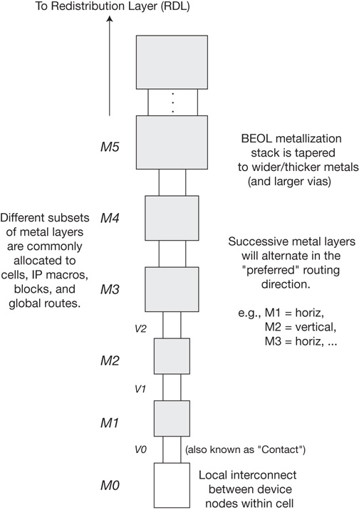
Figure 1.6 Illustration of a BEOL metallization stack, consisting of a specific sequence of metal layers (with corresponding via definitions between layers).
Typically, several metal wire thicknesses are available from the foundry, each with unique electrical characteristics. Thicker metals have larger minimum width and spacing dimensions (and, more recently, are embedded in insulators with lower dielectric constants). Thus, the metallization stack is “tapered.” The foundry provides guidelines on the required and optional number of layers of each thickness type and the appropriate transitions between types. The design team needs to collaborate with the foundry to choose an optimal stack corresponding to the PPA requirements (e.g., 3Mx_3My_2Mz_1Mr for an eight-layer metal design with a top pad metal redistribution layer). The PDK techfile from the foundry is adapted to support this cross-section.
The circuits used for I/O cells are likely to use different transistors to support the higher applied voltages. The FEOL process definition includes the “thick gate oxide” device process module.
All field-effect devices receive a substrate voltage through contacts to the bulk (for nFETs) and n-well regions (for pFETs), using a p-type wafer substrate. A “triple-well” option in the FEOL process allows n-channel field-effect transistors (nFETs) to receive a unique substrate voltage, which is electrically isolated from the voltage applied to the volume bulk substrate of the die.
Analog IP designs may incorporate a variety of optional FEOL process modules:
p-n junction diodes
Resistors, with both (area-efficient) high-resistivity layers and high-precision resistive layers
Bipolar junction transistors (SoC processes are based on field-effect transistors.)
Voltage-dependent capacitors (“varactors”)
Memory array IP layouts are extremely dense and thus are especially sensitive to manufacturing process defects. For SoC designs that utilize large amounts of memory, there is a significant yield risk of a killer defect located in the arrays. The IP vendor may include redundant rows and/or columns in the array implementation, which can be switched in to replace an array location found to be defective in a manufacturing test (see Section 19.3). To enable this yield-enhancing feature, the foundry commonly needs to provide a process option that includes FEOL electrically programmable fuses. (In addition, programming fuses at manufacturing test enables a specific set of personalization information to be embedded in each die.)
The process may offer a unique BEOL metal-insulator-metal (MIM) structure, with a thin dielectric and special intermediate metal plate located between interconnect layers, for an area-efficient decoupling capacitor to connect to the power distribution network.
On-chip inductors are typically implemented using annular coil layouts using the top two BEOL (thick, low-resistive-loss) metal layers, below the pad redistribution metal.
1.4.3 Fabrication Design Rules
The foundry PDK includes documentation that describes the physical layout rules—that is, the design rule manual (DRM). The PDK also includes the EDA tool runset, a sequence of geometric operations that check the layout data against the DRM rule dimensions. All design rule measures are described in reference to a base layout grid (e.g., 0.025nm). All circuit layout dimensions are integral multiples of this grid increment.
The complexity of layout rules has increased dramatically in more recent process nodes due to the requirements to resolve wafer-level exposures using a wavelength greater than the mask dimensions. The design rules for older VLSI nodes primarily consisted of the following:
Minimum width and spacing for line segments (transistors and interconnects)
Minimum area for all shapes (especially applicable to device contacts and inter-level vias)
Minimum overlap/enclosure (e.g., metal over vias)
The sum of the minimum width and spacing is commonly denoted as the pitch for the mask layer.
There were typically no (or very few) design rules that imposed a maximum width/space/overlap, and all dimensions greater than the minimum were allowed to be any integral multiple of the base grid dimension. (The main exception to these general rules pertained to the layout of chip pads on the top metal layer. Pads utilized fixed geometries for the size and top dielectric passivation layer opening for die-to-package pin attach metallurgy.)
As process nodes progressed, manufacturing steps were added to provide improved wafer surface planarization after metal deposition/patterning. These chemical-mechanical polishing (CMP) steps led to the introduction of density-based rules (i.e., minimum density, maximum density, and density gradient limits for the shapes on a CMP metal layer, measured over a layout window of interest). EDA tool vendors needed to add algorithms and runset operations to support these additional design rule requirements.
As SoC designs integrated more memory, the array circuit density became an increasingly influential factor in the chip area. The foundry engineering team pursued specific bit cell designs that were typically more aggressive than the general DRM descriptions for transistor dimensions, contact spacing, and local metal segments. (These special cells in the tapeout database receive unique mask data optimizations.) The memory IP supplier works with the foundry PDK runset team to ensure that these special cells are checked against their array-specific rules and excluded from the general checks applicable to the remainder of the design. The most common methodology approach is to add a “cover shape” over the special cells on a non-manufacturing layer designation specific to array checking. Layout data intersecting the cover is checked against a separate set of array design rules from layout data outside the cover.
As the disparity between mask plate dimensions and exposing wavelength increased, design rules became significantly more complex, including the following:
Metal spacing based on the parallel run length (PRL) to adjacent wires—The greater the parallel run length, the greater the required spacing.
Forbidden pitches—Invalid spacing ranges between (minimum width) wires are due to light diffraction from mask edges interfering to create phantom shapes.
Required non-functional “dummy” shapes—These dummy shapes are placed next to isolated design shapes for better (local) mask data uniformity.
At current process nodes, both the photolithographic resolution and material etch process modules exhibit much greater local sensitivity. A regular pattern improves the fidelity of the fabricated result to the drawn shapes. Dummy data may have a distinct set of width/spacing design rules, as they are non-functional and, thus, non-critical. The layout model needs two separate data designations for a single layer (i.e., functional and dummy) so that specific rule checks can be applied accordingly. During tapeout release, these two designations are merged to a single set of mask data for the layer.
The methodology for physical layout assembly needs to provide support for the addition of dummy data for CMP density and isolated-line checks. The points in the physical design hierarchy where non-functional data is added need to be chosen judiciously. Dummy data added at deep levels of the physical hierarchy may be unnecessary if design rules would be satisfied by integrating the IP layout into higher levels. Conversely, deferring the addition of dummy data until the full-chip SoC layout nears completion may result in design rule errors that are difficult to resolve.
Regardless of where the dummy data is added in the physical design hierarchy, the design rule checking flow needs to include a representative context cell around the cell/block being checked to avoid false errors around the perimeter of the design data, as depicted in Figure 1.7. The context cell includes shapes data for each layer at a “half-design rule space” from the context cell boundary. This ensures that a corresponding half-design rule space is present within the cell/block layout itself so that no design rule errors arise when cells are abutted. The context cell may also include dummy data patterns to provide a larger window around the block perimeter for the layout density checks. And, to provide a representative environment for layout dependent effects upon device behavior, the context cell is also used for parasitic extraction of the block layout prior to electrical analysis.
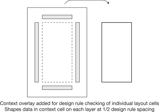
Figure 1.7 Layout design rule verification requires addition of a surrounding layout context cell. The context cell is intended to provide a “representative” environment around the layout to satisfy local spacing checks and minimize the risk of a larger-scale density error when integrating the cell into higher nodes of the physical hierarchy.
Preferred Line Segment Orientations
At current process nodes, the exposing illumination intensity is very non-uniform over the mask field. The illumination pattern (along with the optical corrections applied to the design data when generating the mask) assumes a preferred orientation to the layer data. Design rules are optimized for shapes in the preferred direction, with larger widths and spaces required for any non-preferred “wrong-way” segments. Some layers may not allow any wrong-way segments at all but only rectangles in the preferred direction. EDA tool algorithms thus need to include support for direction specifications in the runset commands.
Multipatterning, Layer Data Decomposition, and Cut Masks
The design rule change with the greatest impact in recent process nodes is the requirement to divide the design data on a single layer into multiple mask plates for fabrication. For example, using 193nm wavelength exposing illumination, with the added resolution benefit of an immersive refracting liquid between lens and wafer, the finest resolvable pitch resolution is ~80nm. A line width plus space less than this dimension would not be printable, necessitating mask data decomposition.
At the most advanced nodes, foundries are working closely with semiconductor equipment and materials manufacturers to transition photolithography for the most critical mask layers to shorter exposing wavelengths, using “extreme ultraviolet” (EUV) sources. This transition involves much more than introducing a new light source and requires significant engineering development focused on new reflective and transmissive mask materials, new mask inspection techniques, new mask data correction algorithms for the source-to-mask-to-wafer optical path, and new EUV-sensitive wafer photoresist coatings, to name but a few. Although shorter exposing wavelengths will help simplify some of the lithographic design rules, multipatterning decomposition will still be required to enable future node scaling.
The scaling of interconnects led to a (lowest-level) metal layer pitch less than 80nm at the ITRS 22nm node. New algorithms were required across the full physical design and checking methodology to decompose layer data into separate masks. Figure 1.8 expands on the data in Figure I.1, illustrating a two-color A/B decomposition and a cyclic layout configuration (at minimum spacing) which is not divisible and is thus a design error.
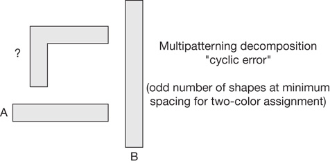
Figure 1.8 The decomposition of mask-layer data into two multipatterning subsets is depicted. A cyclic layout topology is highlighted, which is a layout design rule error.
The number of DRM rules expanded with multipatterning to represent the (min/max) width, (min/max) spacing, (min/max) density, and (min/max) density gradient requirements for each of the layer data decomposition subsets.
Note that the dimensional range of a decomposition algorithm extends well beyond the full size of a shape, unlike the rather limited dimensions associated with all other design rule checks. The color-assignment algorithm needs to verify that no cyclic dependency exists for every shape and all its neighbors. EDA vendors needed to expand their design rule checking runset commands beyond the traditional geometric operations to identify and measure even and odd cycles among (potentially very large) sets of neighboring shapes. If a cyclic dependency is found, changes to wire lengths and/or wire spacing are required. (Although it would be algorithmically feasible to dissect a single shape and assign the dissections to different colors to avoid a cyclic error, this would introduce additional fabrication and electrical modeling issues due to the overlay tolerances between the masks. It would also preclude the foundry from introducing a mask bias specific to the distinct subsets, as highlighted below.)
The impact of multipatterning on the design methodology is pervasive. All physical design checking tools need to be prefaced by a decomposition algorithm before applying shape operations. An interconnect routing tool also needs a decomposition feature to avoid introducing cyclic errors during detailed routing when assigning segments to specific tracks. If the A/B color design rules are symmetric and there is no fabrication “bias” resulting in different electrical characteristics between A and B segments, the cyclic rule checking algorithms need not be exactly the same as that subsequently used by the foundry during mask data processing. If the design rules and/or electrical parameters distinguish between the decomposition subsets, the methodology needs to ensure that a color assignment from the layout engineer or EDA tool is made during physical design and remains as a shape property throughout all verification and analysis flows and, subsequently, in the tapeout release.
Similar to the considerations with the addition of fill shapes data, the methodology for assigning and/or checking decomposition needs to evaluate where in the physical design hierarchy the color property is applied. An individual layout cell may pass decomposition checks but could fail at the higher physical integration levels when adjacent shapes are added. The methodology needs to assess how to ensure that physical assembly does not introduce new decomposition errors. The distance between the physical shapes in a cell and the cell abstract could be increased; layouts could thus be abutted without introducing a decomposition error—at a minor impact in area.
Alternatively, wiring tracks could be pre-assigned corresponding colors. Valid placement locations for a cell or larger IP layout would align the colors assigned to the pin shapes with the wiring track definition. This alternative is emerging as the default for advanced process nodes—that is, the tracks on a multipatterning layer are assigned a specific color, and the shapes aligned to that track (both within cells and for routed wires) are by default assigned that color. There are some subtle nuances to this method, as routed designs may include a mix of minimum and non-minimum width wires on a layer (see Chapter 9, “Routing”).
The shapes in Figure 1.9 illustrate the significance of line-end-to-line-end spacing in terms of the difficulty in resolving the segment ends with high fidelity. To support additional process node scaling, an alternative lithographic and fabrication approach is being applied. Rather than attempt to lithographically resolve two segments with aggressive line-end spacing on a single mask, distinct wires are merged into a single shape, which are then physically separated by a “line cut” masking layer.
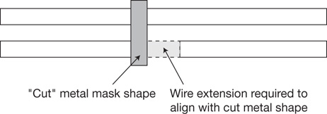
Figure 1.9 The resolution of line-end spacing at advanced process nodes requires merging (and potentially extending) line segments in support of a separate “cut mask” lithography step. Note that the (minimum area) cut mask shape will span multiple tracks. Line ends for wires may need to be extended past their original endpoint to align with the cut mask.
The methodology team needs to collaborate with the foundry support team on the specific mask layer and checking operations in the PDK techfiles and runsets to merge two logically and physically distinct design nets into a single wire plus a cut mask shape. The routing flow needs to ensure that the final wiring track segments will satisfy a subsequent merge-and-cut operation.
As VLSI process nodes continue to scale, the “two-color” multipatterning approach has continued to evolve. One option is to decompose the shapes data into an increasing number of subset colors (continuing with the 193i illumination wavelength). Another option is to accept stringent limits on the flexibility in width and space rules and use process material deposition thickness as a defining dimension. Figure 1.10 illustrates a self-aligned, double-patterned (SADP) fabrication flow. The number of mask layer exposures is reduced with SADP. In return, the post-etch width of the underlying material is fixed by the dimensions of the “sidewall spacer,” a dielectric material isotropically deposited and anisotropically etched.
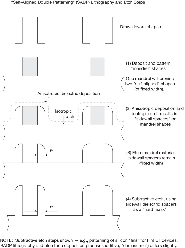
Figure 1.10 A self-aligned, double-patterned process flow utilizes the deposition of a sidewall spacer on a patterned shape as a subsequent masking layer. The final (fixed) resolution of the etched material is defined by the width of the spacer.
If the final etched material is a dielectric, the subsequent deposition of a metal will result in a fixed space between adjacent wires. For the case of a FinFET transistor (discussed in the next section), the etched material is the silicon “fin” used for the device substrate; in this case, the thickness of the silicon fin is fixed by the SADP process. Successive applications of this technique offer a self-aligned, quad-patterned (SAQP) flow for continued dimensional scaling; the original SADP-etched material serves as the mandrel for a subsequent SADP process sequence.
1.4.4 Bulk CMOS Technology
The origins of IC logic technology began with bipolar transistor circuit configurations (e.g., emitter-coupled logic [ECL]), transistor-transistor logic [TTL]). The emphasis on VLSI scaling resulted in the emerging process maturity of metal-oxide-semiconductor field-effect transistors (MOSFET) and specifically logic circuits consisting of complementary n-channel (nFET) and p-channel (pFET) device topologies, or CMOS. (There was also a short-lived logic technology offering merging CMOS logic devices with bipolar transistor output drivers, but BiCMOS did not continue through subsequent process node scaling.) This section briefly reviews the prevalent CMOS process technology options, with an emphasis on how their different characteristics impact the design methodology.
Advanced fabrication technology research is being pursued to define transistor topologies that will continue to enable scaling for the 5nm ITRS node and below—for example, (horizontal or vertical) nanowires with the device input gate “all around” the nanowire semiconductor. Regardless of the likely emergence of new transistor materials and topologies to support the demand for PPA improvements, the methodology considerations for those technologies will have much in common with the three CMOS processes highlighted in this section.
The traditional CMOS process technology utilizes a silicon wafer substrate as the foundation for fabrication of n-channel and p-channel FETs. Specifically, Figure 1.11 illustrates a cross-section of the two device types. A starting p-type bulk wafer consists of an epitaxial crystalline layer grown on a substrate; the epi layer has a smaller concentration of introduced p-type impurities, and the substrate has a much higher concentration. The pFET requires an n-type background material, which is realized by the introduction of n-type impurities, creating an n-well in the p-epi layer. Electrical isolation between device nodes is improved by the addition of a recessed oxide, or “shallow trench” oxide isolation (STI), dielectric introduced into the substrate.

Figure 1.11 Silicon wafer cross-section for nFET and pFET devices used in complementary metal-oxide-semiconductor (CMOS) logic circuits.
The nFET and pFET devices consist of four terminals: gate, drain, source, and substrate. The input gate terminal is isolated from the FET channel by a thin gate oxide dielectric. The conductivity between drain and source is modulated by the voltage difference between gate and source (Vgs), with an indirect influence of the source-to-substrate voltage difference, Vsx. (The substrate contacts to the p-epi for an nFET and the n-well node for the pFET are not shown in the cross-section figure but will be added liberally to circuit layouts.)
The electrical charge carriers in the surface channel region with Vgs = 0V isolate the drain and source nodes, denoted as the “accumulation” region of transistor operation. As the input voltage |Vgs| increases—Vgs positive for nFETs, Vgs negative for pFETs—the charge carrier concentration in the channel changes from the majority carriers of the substrate to the minority carriers of the source/drain nodes. A depletion region is initially formed in the channel as |Vgs| increases, where the concentration of free charge carriers is reduced. The electric field across the depletion region provides the drift transport for any injected carriers. As |Vgs| increases further, a concentration of minority free carriers is present at the surface channel. The conductivity of the channel between drain and source increases through “weak inversion”—with Ids at leakage current levels—to “strong inversion.” The input gate voltage where the minority carrier concentration in the channel is (roughly) equal to the majority carrier substrate concentration in the substrate is defined as the transistor threshold voltage, Vt:
As a CMOS logic input signal transitions between logic voltage levels, the drain-to-source conductivity of the nFET and pFET devices receiving that logic gate input transitions in complementary fashion, with one device reaching inversion while the other reverts to accumulation. During this input transition, there is a “cross-over” period when both devices are conducting simultaneously, as depicted in Figure 1.12. This cross-over interval results in significant power dissipation between VDD and ground and detracts from the device current to the interconnect loading to propagate the logic gate output value.
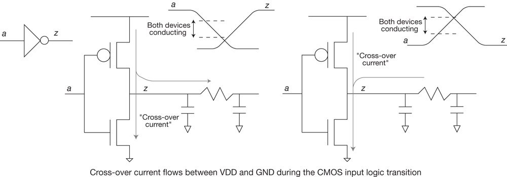
Figure 1.12 An input transition to a CMOS logic gate results in complementary behavior of the nFET and pFET devices. A cross-over current flows within the circuit during the interval when both devices are conducting.
A key methodology step is to ensure that the input logic signal transition time does not exceed a suitable limit to minimize the cross-over power dissipation; otherwise, buffering of the circuitry driving the input would be necessary.
With the evolution of VLSI technologies, the device channel length has been the benchmark for the process node definition. The “drawn” channel length in layouts has typically been the same as the node name (e.g., L_drawn = 10nm). The actual “electrical channel length” differs from the drawn length as a result of the process bias—a combination of lithography, deposition/etch, and impurity introduction steps that result in a wafer-level dimension that differs from the drawn dimension. The transistor simulation models in the foundry PDK incorporate this bias so that the circuit netlist with drawn values provides accurate results.
The scaling of device dimensions in advanced process nodes has also necessitated reducing the applied supply voltage to keep the electric fields between device gate and channel through the thin oxide below the reliability concerns of dielectric breakdown. Similarly, the electric fields between source/drain and substrate need to observe limits associated with p–n junction reverse bias avalanche breakdown. As supply voltages have scaled, from 5V at the 2-micron node to sub-1.0V for current processes, the magnitudes of the threshold voltages have also necessarily been reduced to maintain circuit performance. As a result, devices with a Vgs = 0V input may indeed be in the weak inversion mode. The subthreshold leakage currents in a CMOS logic circuit (i.e., Ids_leakage for Vgs < Vt) are a major concern for the (static) power dissipation of SoCs intended for mobile applications. The electric field between drain-and-source of an “off” device in weak inversion (i.e., |Vd – Vs| = VDD, Vgs = 0V) is also a reliability concern, potentially resulting in device punchthrough current. As VDD supply voltage scaling has slowed with successive nodes, fabrication processes have transitioned to an effective gate length significantly greater than the drawn length.
A fabrication option is commonly provided that locally varies the majority surface carrier concentration in the channel and thus provides different transistor Vt values. (The previous section highlights library standard cells using LVT, SVT, and HVT devices.) A low-Vt device, with fewer (net) majority carriers in the channel switches sooner upon an input transition and thus provides a faster overall logic propagation delay. The trade-off is that the low-Vt device has increased subthreshold leakage current when the device is off. In the weak inversion mode, the Ids subthreshold current is exponentially dependent upon the Vgs – Vt voltage difference. As illustrated earlier in the log-linear plot in Figure 1.3, a low-Vt device has an exponential increase in leakage current compared to a nominal “standard” Vt device. The PPA optimization steps in the methodology flow evaluate performance versus (static) power dissipation when considering a logic cell swap between circuit implementations with different Vt devices.
Body Effect and Vt Dependence on Vsx
The device channel operating mode depends on the source-to-substrate voltage difference. As the magnitude of |Vsx| increases, the magnitude of |Vt| also increases. To first order, this is a square root dependence; that is, |Vt| is proportional to (|Vsx|**0.5). This body effect has a significant impact on circuit behavior and the overall design methodology.
One benefit of the body effect is that it offers an opportunity to readily provide a sleep state to an IP core. For example, application of a pFET n-well voltage above the VDD supply rail results in a higher |Vtp|, as illustrated in Figure 1.13. The leakage currents in a static logic network (e.g., with inactive clocks) are significantly reduced with this body bias.
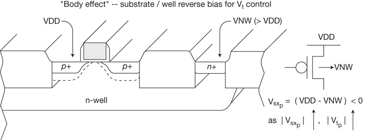
Figure 1.13 An n-well voltage above VDD applies a body bias to pFET devices, increasing the |Vt|, and significantly reducing the static leakage current.
Commonly, the n-well bias connection uses the VDD rail in the cell template. If a separate n-well voltage rail distinct from the logic VDD supply is provided, and a power management controller is available to generate a unique supply above VDD, the body effect circuit topology is a relatively straightforward means to achieve a reduced-leakage sleep state. The complementary nature of CMOS processes implies that a similar body bias implementation is available by applying a negative voltage to the p-type bulk connection for nFET devices; the nFET leakage currents are reduced with (Vs – Vx) > 0V.
Note that there is a significant capacitance Csx that would need to be charged/discharged to use body bias to transition to/from the low-leakage condition. Also, there is a strict limit on the magnitude of the source-to-substrate voltage bias that can be applied due to limits on the electric field present in the surrounding depletion region. Additional fabrication steps can be taken to increase the body bias limit, with tailoring of majority carrier concentration near the source/drain nodes and below the surface channel, including a “lightly doped drain” (LDD) profile near the channel surface, halo implants at the source/drain device nodes, and buried layers of higher-majority-impurity concentration in the bulk substrate. Nevertheless, the effectiveness of body bias in scaled VLSI process nodes for bulk CMOS is reduced due to the applied voltage and electric field limits.
Another characteristic of the body effect is the impact on circuit performance for FET devices connected in series. Figure 1.14 illustrates the circuit topology for the series nFET devices from a three-input NAND gate. (The pFETs connected to the logic gate inputs in the complementary parallel topology are not shown in the figure.) Series devices need to be significantly wider—typically, implemented as parallel fingers—to reduce the nominal “on resistance,” as depicted earlier in Figure 1.2. A logic input transition that results in a current through a series nFET stack is illustrated in Figure 1.14.
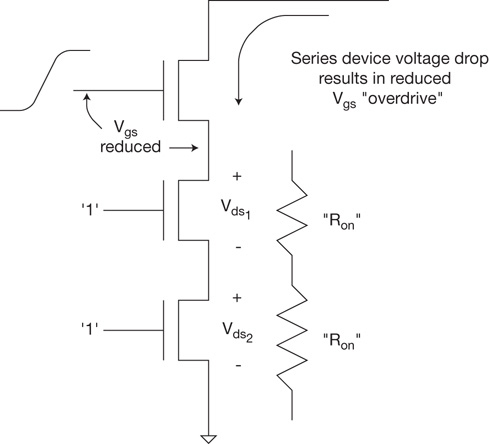
Figure 1.14 A logic transition current through a series stack of devices generates a Vsx voltage difference at intermediate nodes, increasing the device |Vt| and reducing the stack conductivity.
The transient current results in a Vds voltage across the resistance of the individual devices in strong inversion; the voltage drop at the intermediate nodes in the stack provides an inherent body effect. During this logic transient, the switching device conductance decreases, adversely impacting the logic transition delay.
In the bulk CMOS substrate device cross-section in Figure 1.15, there are additional characteristics of note.

Figure 1.15 Electrically, the device gate input connection is a distributed R*C network, as the input transition charges the channel capacitance through the resistive gate. Circuit simulation models for the device reflect this behavior using an “effective” Rg element. Additional process steps are introduced to add to the silicon volume of the source/drain nodes to reduce the series resistances Rs and Rd in the device model. The “raised” nodes incorporate a high impurity concentration (n-type for nFETs, p-type for pFETs) during the silicon growth step.
Low-Resistivity Gate Material
The FET gate is more accurately modeled as a distributed R*Cchannel network. A transient on the device input propagates down the resistive gate, charging the local channel capacitance. Various process options are available from the foundry, with different gate material resistivity (e.g., poly-crystalline silicon with a high impurity concentration, polySi with a metal silicide top layer, refractive metals). At advanced process nodes, to reduce the impact of the increase in gate resistance with gate length scaling, a metal gate material is used. The device models include an “equivalent” parasitic Rgate so that simulation with the model device capacitances more accurately represents the input transient.
The contact potential between the gate material and the gate oxide dielectric also helps define the threshold voltage of the device. In addition, the foundry offers local device Vt options through the introduction of a small concentration of impurities at the channel surface, using a threshold implant mask.
Raised Source/Drain Nodes
Complex process steps are incorporated to increase the silicon volume of the source/drain nodes, concurrently introducing minority carrier impurities. The device model includes parasitic resistances Rs and Rd in series with the device channel. The high-impurity concentration “raised” nodes reduce this parasitic resistance. The top of the source/drain nodes typically includes a metal-silicide material layer to further reduce the source/drain resistivity. The method for introducing the raised source/drain nodes may also transfer compressive (pFET) or tensile (nFET) stress into the silicon crystal lattice of the device channel. These lattice forces are used to improve the inversion minority carrier mobility, improving the Ids device current for a given Vds voltage difference.
Spacer Dielectric Between Gate and Raised Source/Drain Nodes
In addition to the Rs, Rd, and Rg elements, another key device characteristic is the parasitic effects of Cgs and Cgd. The transient operation of the device through accumulation and inversion involves charging the internal gate-dielectric-channel capacitance, Cox; in the device model, the voltage-dependent Cox is allocated between the elements Cgs, Cgd, and Cgx. The fixed parasitic capacitances in the device structure are added in parallel to the internal Cgs and Cgd elements (see Figure 1.16).

Figure 1.16 Capacitances Cgs, Cgd, Cgx, Csx, and Cdx are included in the device model to reflect the gate-to-channel input capacitances, the source/drain junction capacitances to the substrate, and the configuration of the dielectric materials between the device nodes. For simplicity, raised source/drain nodes are not shown in the figure, but their topology contributes significantly to Cgd and Cgs.
The dielectric surrounding the gate defines the parasitic capacitances added to Cgs and Cgd. The materials choice and thickness of the “spacer” is a critical process optimization. A larger spacer reduces the Cgs and Cgd parasitics but adversely impacts the layout pitch for the gate-to-device contact-to-gate dimension. A smaller spacer improves the contacted gate pitch but adversely impacts the capacitive parasitics.
In Figure 1.16, also note that there is a (fixed) Cgs and Cgd parasitic contribution due to the gate-to-source and gate-to-drain overlap at the channel surface. Although it is required to ensure a continuous, conducting channel in inversion, significant process engineering development resources are applied to reduce the extent of this overlap.
From a design methodology perspective, the main implications of selecting a bulk CMOS fabrication process are as follows:
All circuit simulation flows need to ensure that the parasitic elements—Rg, Rs, Rd, Cgs, Cgd, and Cgx—are enabled and accurately reflected in the device model, using data from the foundry process PDK.
The primitive cells in the IP library with a high fan-in (i.e., a large number of devices in series) are logically powerful. However, these cells have the disadvantage of requiring large-width devices to reduce the Ron device resistance. There is also the performance impact of the transient body effect. The SoC methodology and design teams need to evaluate the PPA benefits of these cells relative to design goals and determine if any should be excluded from the available cell library. (To some extent, the IP cell library provider has already made this decision in terms of the diversity of its logic offering—for example, “no logic gates with series stack height greater than three.”)
If the SoC design team intends to utilize the (limited) back bias device characteristic for leakage control, this introduces additional voltage settings for electrical analysis flows. The addition of a distinct back bias rail from the circuit VDD (or ground) rail impacts the definition of the cell template and available routing tracks. Power distribution network analysis needs to include the additional back bias rail (e.g., the I*R voltage drop on the rail due to leakage currents, the transient rail currents to/from sleep state transitions). A special layout physical design rule check applies for the back bias rail, as the voltage difference between this rail and internal circuit nodes exceeds VDD. The methodology team needs to review with the foundry how the “high voltage differential” spacing checks are to be applied in the PDK runset operations and ensure that the back bias rail connections are designated with the corresponding property.
There are two additional very important reliability considerations for selecting a bulk CMOS process:
Latchup—Adjacent nFET and pFET devices in a bulk CMOS process introduce a p-n-p-n junction topology, typically associated with a silicon-controlled rectifier (SCR). If a transient (capacitive-coupled) event were to inject sufficient carriers into the “triggering input,” and if the current gain of this composite structure were greater than one, the SCR action would result in a high-parasitic, sustained current; this latchup condition must be avoided. Foundry layout design rules provide guidelines on the density of well/substrate contacts and provide requirements for separate injected charge collection “guard rings” surrounding circuits subject to capacitive triggering. Both precautions reduce the likelihood of a latchup event. A latchup analysis methodology flow and a set of circuit and layout checking criteria is needed for a bulk CMOS design (see Section 16.2).
“Soft errors”—The exposure of an SoC design to cosmic radiation and/or close proximity to radioactive material decay results in the trajectory of a high-energy particle toward the bulk substrate. As the particle traverses through a high electric field depletion region near a device source/drain, lattice collisions generate free carriers that are swept to a device node by the field. The resulting collected charge on the node introduces a voltage differential. If the active current at the node is small, this differential could result in erroneous (detectable) circuit behavior. As the error is not due to a permanent defect, such as a dielectric breakdown, it is denoted as a “soft error.”
The most prevalent example of circuits subject to soft errors in bulk CMOS is a node dynamically storing charge, such as an array location in an embedded dynamic RAM IP block on an SoC. The lack of an active current from the dynamic node results in a high charge collection/retention efficiency. SRAM bit cells and flip-flop circuits also rely on very-low-current feedback loops to retain state; these circuits are also susceptible to soft error event upset.
The foundry adds features to the bulk CMOS process to reduce the sensitive free carrier generation and collection volume when a particle strike occurs. For example, devices are commonly fabricated using a bulk substrate with a thin, low-impurity concentration epitaxial crystalline surface layer, as depicted in Figure 1.11. Free carriers generated in the high-impurity concentration bulk have a high recombination rate rather than drift to a sensitive circuit node.
Even with these process features, critical design and methodology steps are needed to reduce the soft error rate. The layout design area of any dynamic or weak feedback node needs to be minimized to reduce the collection volume. The methodology flow needs to include an analysis of the probability of a single-event upset (SEU) based on the sensitive layout collection volume, anticipated particle flux and energy distribution, and carrier generation probability (see Section 16.4). The resulting SEU probability calculation is used by the design team to determine the need for additional parity generation and/or error detection and correction (EDC) logic on sensitive memory array word or stored register values.
The IP vendor has to address a trade-off when designing a function with SEU-sensitive circuits, as the end customer SoC applications could be quite varied. The addition of EDC functionality reduces the SEU susceptibility, at the cost of additional area and performance, which may detract from the marketability for very cost-sensitive end products. Medical and mil-aero applications have the most stringent SEU correction requirements. Indeed, IP qualification for a mil-aero application is likely to require more than the typical stress testing of the IP from a foundry’s shuttle lots. Special electronic testing facilities offer a high radiation flux exposure chamber similar to a high-altitude environment to more accurately evaluate whether SEU correction methods are sufficient; this additional qualification adds considerably to the IP development cost.
1.4.5 Fully Depleted SOI (FD-SOI) Technology
Silicon-on-insulator (SOI) process technologies have been available in production for several VLSI process generations. As illustrated in Figure 1.17, a thin silicon layer with “near intrinsic” (very low) impurity concentration is used to fabricate the devices, similar to a bulk CMOS process. In this case, a dielectric layer exists between the devices and the substrate. The presence of a dielectric introduces several differences to a bulk CMOS process:
The bulk CMOS process parasitic reverse-bias leakage currents for the p-n junctions between source/drain and bulk/well nodes are eliminated.
The parasitic Csx and Cdx capacitances are now a silicon-dielectric-bulk structure rather than the p-n junction capacitance.
The body effect is now controlled by the dielectric capacitance between the substrate and device channel.

Figure 1.17 In this cross-section of a fully depleted silicon-on-insulator device, note the dielectric layer between the device channel and the wafer substrate. The substrate/well connections are etched through the thin silicon and dielectric top layers. (The well profile below the dielectric layer is not shown in the figure.)
As VLSI technologies have scaled, the thickness of the SOI process silicon device layer has also been reduced. At current process nodes, the depth of the source/drain impurity regions extends throughout the silicon layer. The silicon layer and device gate oxide thicknesses are selected such that the gate input has a strong electrostatic control over the channel. For example, the silicon layer thickness is roughly one-third of the device electrical length (distance between drain and source nodes). As a result, the device current falls quickly as the gate input turns off, which reduces CMOS cross-over current and improves logic circuit performance. This is expressed as the device model parameter known as the sub-threshold slope—mathematically, S = dVgs/dIds, (Vgs ~ Vt). Alternatively, this device measure is expressed as the difference in Vgs that results in a 10X decade reduction of Ids in the sub-threshold region—for example, S = 70mV. The gate oxide-channel electrostatics are such that the channel volume is fully depleted of majority free carriers when the device is “off”; this specific SOI process option is denoted as FD-SOI.
The FD-SOI process has some unique characteristics:
The elimination of source/drain junction leakage currents and the improved device sub-threshold slope result in lower overall leakage power than a comparable bulk process node.
Latchup is effectively suppressed, as p-n-p-n junctions are absent.
The dielectric layer between device channel and bulk substrate offers the opportunity to apply either a negative or positive body bias to the device.
As with a bulk process, a negative bias increases |Vt|, reducing leakage currents further. The magnitude of the applied negative body bias can be larger than in a bulk CMOS process, as it is limited by the electric field across the dielectric rather than the electric field between the source/drain and bulk junctions.
The SOI dielectric also offers the possibility of a (limited) forward body bias relative to the channel, reducing |Vt| and providing an active device current increase. (A forward body bias in a bulk CMOS process is discouraged due to the forward bias on all p-n junctions.) A performance boost could be realized from forward body bias, either temporarily or from an adaptive controller that generates a bias to minimize performance variations over process, voltage, and temperature ranges.
Multiple Vt device variants are implemented differently in FD-SOI than for a bulk process, as the controlled introduction of additional impurities into the very thin SOI channel is more difficult. Instead, the contact potential between the materials can be varied (i.e., the gate-oxide, oxide-channel, channel-insulator, insulator-well interfaces). For example, the (metal) gate composition can be altered to adjust the gate-to-oxide contact potential. Alternatively, the impurity concentration (and type) in the local well below the insulator can be modified to adjust the insulator-to-well potential. Nonetheless, it is more complex (and expensive) to introduce device Vt options in FD-SOI than for a bulk process.
The volume of high-impurity concentration source/drain nodes is constrained by the thickness of the silicon device layer; Rs and Rd are significant model parasitics in FD-SOI. As with a bulk process, raised source/drain node process engineering is pursued. Nevertheless, there remains a series resistance contribution to Rs and Rd from the thin FD-SOI silicon layer.
The physical layouts of bulk CMOS circuits are relatively easy to migrate to an SOI process (at the same node). As the device channel cross-sections between bulk CMOS and SOI are similar, the device and contact layouts are likewise comparable.
To transition a bulk CMOS layout to an FD-SOI equivalent, specific layout migration support is needed for bulk CMOS Vt device variants and bulk/well contacts.[12] (As mentioned earlier, in FD-SOI, the well contacts require etching through the top silicon and insulating layers.)
Despite the relative ease of device layout migration, the FD-SOI process does not easily support the addition of some circuit elements used in bulk CMOS analog IP (e.g., bipolar npn transistors, p-n junction diodes).
With FD-SOI, unlike with bulk CMOS, there is no inherent (vertical) p-n junction with precise impurity concentration profiles. Analog IP design requires adaptation to the available circuit elements. (This also applies to other IP circuits using p-n junctions, such as ESD protect structures and temperature sensors.) For example, a lateral p-to-intrinsic-to-n junction may be available from the foundry by introducing different impurity types for the source and drain nodes, separated by the intrinsic device channel. Alternatively, an FD-SOI nFET device with the gate input tied to the drain as anode with the source as cathode provides a similar two-terminal structure.
The methodology for an FD-SOI design is similar to that for a bulk CMOS design. A foundry may offer both processes at the same node, and an SoC design team may want to pursue a competitive PPA analysis of critical IP blocks. Layout migration may be a new flow to add to port existing bulk layouts to FD-SOI for re-extraction and performance characterization.
The increased range of (negative and positive) body bias in FD-SOI offers a variety of operating mode conditions and requires a review of the multi-corner, multi-mode (MCMM) analysis matrix (see Section 10.2). As with bulk CMOS designs, the applied FD-SOI body bias requires support for high-voltage signal spacing checks.
1.4.6 FinFET Technology
The FD-SOI device technology is based on a topology in which the gate input voltage has a strong electrostatic influence on the thin, fully depleted silicon layer. An alternative topology that also provides this electrostatic impact is realized by the FinFET device, whose cross-section is illustrated in Figure 1.18.
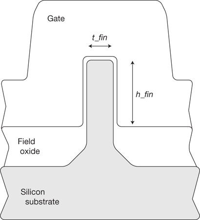
Figure 1.18 FinFET device cross-section. The device gate length (and direction of Ids current flow) is perpendicular to the page.
The device channel volume is defined by a vertical pedestal, or fin, of silicon, that is defined by a sequence of process steps:
Silicon wafer etch using SADP to define a uniform fin thickness, based on the width of the spacer. (Note that the silicon etch is deeper than the final fin height.)
Dielectric deposition
Wafer polish
Precisely controlled oxide etch-back to expose the fin
The device gate oxide is grown on the fin, followed by gate patterning. The final device consists of a common gate covering all three exposed facets of the fin. The device current between drain and source nodes flows laterally through the fin, as depicted in Figure 1.19.

Figure 1.19 FinFET device current flow through the vertical fin. The figure depicts three fins connected in parallel. The gate input traverses all the fins. A local metal shape connects the parallel drain nodes, and another local metal shape connects the parallel source nodes (not shown in the figure).
Note that the effective width of the device channel is defined by the fin geometry: Current flows through a silicon surface channel that spans the two vertical sides and the top of the fin. Thus, the effective device width of a single fin is W = ((2 * h_fin) + t_fin). The fact that the FinFET width is not a continuous circuit design/layout parameter but rather is quantized in multiples of (2h + t) has significant impact on the methodology flow (as discussed shortly). For process simplicity, the fin height and thickness are (nominally) uniform across the wafer. In addition, no combination of fins and planar FET devices are typically offered. Also, for advanced lithography VLSI process nodes, there is typically very little flexibility allowed in drawn gate length.
The fin thickness is sufficiently small, such that the fin volume for an “off” device is fully depleted of majority carriers. The subthreshold slope of the FinFET is attractive, much as with FD-SOI. There is a bulk drain-to-source leakage current path in the base of the fin, at the interface between the gate and thick dielectric. Additional process steps are pursued to alter the impurity concentration in the base of the fin to reduce this leakage current and reduce the risk of drain-to-source punchthrough current at a high Vds voltage. Although FinFET devices could be fabricated using an SOI wafer substrate, where the silicon layer thickness above the insulator would define the fin height, all FinFET high-volume fabrication is currently using bulk silicon substrates.
FinFET Characteristics
There are unique characteristics of device variation in FinFET fabrication as compared to planar (bulk or FD-SOI) devices:
Fin profile—The silicon pedestal etch and subsequent oxide etch-back process steps to expose the silicon fin introduce a source of variation in the fin height and thickness across the wafer. Actually, the corners of the fin are not rectangular but intentionally rounded to avoid high gate-to-channel (horizontal and vertical) electric fields at the top of the fin (see Figure 1.20). The initial FinFET device models assumed a rectangular profile. The PDK model parameters (and statistical variations) required fitting the model to fabricated silicon characterization data. More recently, extended device models that accept a more general (non-rectangular) fin profile have been developed.[13,14]
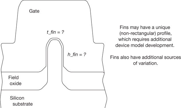
Figure 1.20 FinFET corner profile. The fin cross-section is typically closer to being a trapezoid than to being a rectangle.
Vt variation (SVT device)—The silicon fin utilizes a very low (near intrinsic) background impurity concentration, resulting in low threshold voltage variation in the “standard” Vt device.
Fin surface roughness—The FinFET-specific process steps result in a risk of vertical surface roughness and subsequent variations in local oxide thickness and device current.
Gate line edge roughness (LER)—Although planar devices are also subject to LER gate length variations along the width of the device, the FinFET gate must traverse the vertical topography of the fin, which is a difficult patterning process step to control.
Gate oxide thickness at the FinFET base—At the base of the fin, the gate material interface transitions from the thick dielectric over substrate to the thin device oxide layer. Ideally, this transition would be abrupt, restricting channel current to the vertical fin surface. As mentioned previously, there is (active and sub-threshold) device current along the base transition that is more difficult to model.
FinFET Advantages
The FinFET technology offers some significant advantages over the planar device processes:
Layout density—The vertical fin provides an effective device width of (2h + t) in a drawn dimension of width t. To realize a larger device width, multiple fins are connected in parallel, as shown in Figure 1.21. A single gate input spans all fins, and local metal interconnects short together the individual source and drain nodes. Figure 1.21 illustrates three fins in parallel, with a total width of W = 3 * (2h + t), in a drawn width of (3t + (2 * space_fin)). Assuming an appropriate fin height relative to the fin space, the total device current density is higher than for a planar FET layout. As mentioned previously, the total FinFET device width is not a continuous dimension but rather is a multiple of the individual fin effective width.
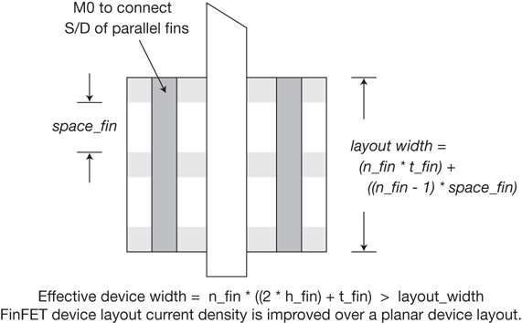
Figure 1.21 Multiple fins connected in parallel. The device width is an integral multiple of (2h + t). The current density is improved for FinFETs compared to planar (bulk or FD-SOI) devices, as the effective width of multiple fins is greater than the layout width.
Note that the fabrication process design rules impose strict requirements on the fin positioning. The space between fins is fixed. Fins for separate devices throughout the die are “on grid”; the fabrication process for the silicon pedestals does not readily support staggered fin alignment in adjacent cells. The design rules may impose limits on the number of parallel fins per device. Even if there are no stringent lithographic limits, the parasitic gate resistance (Rg) and parasitic capacitances (Cgs and Cgd) adversely impact an input transient for a large fin count. The maximum number of fins may also be constrained by the local metal interconnects: The increased current density through these metals introduces a reliability concern due to electromigration (see Chapter 15). As with planar device technologies, I/O pad driver circuits still require many device fingers in parallel to provide the large transient currents rather than using very large fin counts per device.
Very weak body effect— The FinFET topology, the strong electrostatic control of the gate over the active fin volume, and the punchthrough stop impurity introduction below the fin imply that the substrate voltage has little influence on the FinFET device’s behavior. Unlike the bulk CMOS and FD-SOI planar devices, the body effect for FinFETs is very weak. Although the subthreshold leakage and subthreshold slope are attractive features, the application of the body effect to further optimize static leakage power in a sleep mode is not as effective for FinFET devices.
The lack of a body effect also implies that the series device stack performance penalty is reduced. The combination of the improved layout current density and low series stack penalty suggests that a FinFET IP library may incorporate base logic cells with higher fan-in (series stack height) than for a planar process.
Multiple Vt device variants available—The local introduction of additional impurities into the fin or an alternative metal gate composition with a different oxide contact potential enables multiple FinFET device Vt options at a relatively low additional process cost.
FinFET Constraints
For IP circuit designers, FinFET technology introduces new constraints:
Parasitic Cgs, Cgd, and Cgx—The topography of the gate traversing multiple parallel fins adds parasitic capacitances, as highlighted in Figure 1.22. The improved layout current density is mitigated somewhat by the additional device input capacitance.

Figure 1.22 Illustration of the additional parasitic capacitances Cgs, Cgd, and Cgx for the gate input traversing over the dielectric between parallel fins. There are additional contributions from the gate to fin sidewall capacitance (Cgs and Cgd) and the gate over thick oxide between fins to the substrate (Cgx).
The optimum FinFET circuit sizing to reduce total logic path delay is an intricate function of device drive strength, internal capacitances, and the external loading from signal interconnects and fanout gate inputs. For small interconnect loading, increasing the logic gate drive strength along a path quickly reaches a “gate-limited” condition, where increased currents are countered with comparable increases in internal and gate fanout capacitive loads.
Quantized device effective width—The primary design impact of the FinFET technology is the limit on device widths, in multiples of the fin dimensions (2h + t). Analog circuits no longer have the ability to arbitrarily tune to specific bias currents. Fortunately, many analog designs rely on device matching to a greater extent than the absolute magnitude of the bias currents. The low variation in the FinFET standard Vt (with intrinsically doped fins) and the weak body effect offer good differential matching characteristics.
Flip-flop circuits often rely on weak feedback of the output value to an internal node to retain state. The feedback circuit needs to provide necessary node leakage currents yet must be easily overdriven when writing a new flop value. The smallest single fin device width (and limited gate length options) may result in a stronger feedback circuit than would be needed to sustain internal circuit node voltages and, thus, higher internal switching power dissipation for these flip-flop circuit types.
The FinFET width constraints also have a strong influence on SRAM bit cell design. For a planar process, the sizes of the cross-coupled inverters and word line access devices in the bit cell are optimized for PPA, for a target number of bit cells located in a column between a differential pair of bit lines. The SRAM bit cell offerings in a FinFET process technology are limited by the quantized fin width. A high-density bit cell could be designated by the foundry as using one fin throughout for access, pullup, and pulldown transistors (e.g., a 1-1-1 cell). A high-performance option could be implemented with (asymmetric) device widths, such as the 2-2-1 design depicted in Figure 1.23. The memory array IP provider integrating the foundry FinFET bit cell is constrained by these sizes.
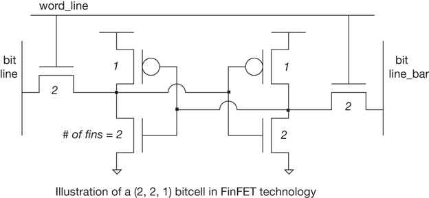
Figure 1.23 FinFET 6-T SRAM bit cell design example, illustrating the device widths as an integral numbers of fins (all with minimum gate length).
These FinFET bit cell characteristics may introduce a unique SRAM (sub-block) architecture if the high-density or high-performance array circuit design results in a different number of bit cells per column than would be defined for a planar process.
Electromigration and self-heating—The higher FinFET layout current density implies that the local metal wires and contacts will also be carrying a greater current density. The risk of electromigration failure in these segments is increased. The fin profile also results in a constrained thermal path. The (Ids * Vds) power dissipation in the device channel generates heat; the energy flow follows the path of low thermal resistance. In a bulk CMOS process, the silicon substrate provides a low thermal resistance under the channel. In an FD-SOI process, the thin insulator layer is less thermally conductive, and an increased fraction of the heat flow traverses through the device nodes. For a FinFET process, the relative dimensions of the fin (with the surrounding dielectrics between fins) results in an inefficient thermal path to the silicon substrate. A large percentage of the thermal energy flows through the device nodes and interconnects. This energy results in a local self-heating temperature rise. The activation of metal atom transport associated with electromigration in a current-carrying segment increases exponentially with temperature. Electromigration analysis needs to include the corresponding temperature rise from active device self-heating in the neighborhood of the interconnect segment.
FinFET Design Methodology
The methodology for IP design in FinFET technology also must address several new constraints:
All cell placements must result in the underlying device fins being on-grid.
All device schematic widths must be a multiple of Nfin * (2h + t); all device layout shape widths must be (Nfin * t) + ((Nfin – 1) * s).
For simplicity, the schematic symbol notation for FinFET devices could replace the (W, L, N_fingers) parameters for bulk devices with (Nfin, L, N_fingers); indeed, the PDK device simulation models are likely to be defined using Nfin. To reduce visual complexity, the fin process lithography layer need not be explicitly drawn in circuit layouts; a single device area shape on-grid and of vertical dimension equal to (Nfin * t) + ((Nfin – 1) * s) could equivalently represent the parallel fins. Layout parasitic extraction and design rule checking flows would internally convert to the required fin geometry.
Inactive gates drawn on the edge of the active area are required for litho and process uniformity.
As with the planar process technologies, it is necessary to expand the silicon volume of the drain and source nodes to reduce Rd and Rs. A spacer dielectric is again deposited on the sidewalls of the gate. The FinFET geometry is unique, as the additional silicon grows in multiple (crystalline) directions off the exposed source/drain fin surface. To improve process uniformity, the step for expanding the fin nodes benefits from a symmetric topography of gate dielectric spacers on both sides of the node. As a result, it is necessary to add a dummy gate at the edge of an active area. The spacers on both sides of the source/drain fin define the extent of the raised node. Figure 1.24 illustrates the addition of a dummy gate at the edge of an active area. The figure also illustrates dummy gates inserted adjacent to the active device areas for improved photolithographic uniformity.
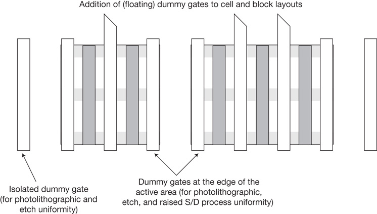
Figure 1.24 FinFET device layouts require “dummy gates” at the edges of active areas for lithographic and fabrication uniformity; the gates on the active device edge are electrically floating. An alternative design style would merge the dummy gates at the edges of separate active areas, tied off to electrically isolate adjacent nodes.
The dummy gate on an active area edge requires unique methodology consideration. Device recognition algorithms need to exclude this non-functional device from layout-to-schematic (LVS) correspondence checking. Layout parasitic extraction needs to include the parasitics associated with this abbreviated device (e.g., a “three-terminal” FinFET instance in the extracted circuit simulation instance with floating gate and no source node).
To minimize the overhead of these dummy gates, layout designers may seek to consolidate active areas, merging adjacent FinFETs. In this case, the single dummy gate between devices must be tied to an “off” voltage. The layout analysis methodology must recognize the presence of the off device isolation and apply the correct interpretation for various flows (i.e., a non-functional device for layout-versus-schematic correspondence checking yet included in layout parasitic extraction for the additional parasitics and leakage currents between adjacent circuit nodes).
Extending this approach further, it would be feasible to use off devices between adjacent library cells. The cell template would need to readily support connecting gate inputs to the “off” logic value power rail for both nFET and pFET devices. Special “context cells” would need to be abutted when analyzing an individual cell to estimate the final environment. Special “row end” non-functional cells would need to be added to the placed layout. A complication of the use of off devices between cells arises when abutting cells with different numbers of fins in the active areas, as depicted in Figure 1.25.
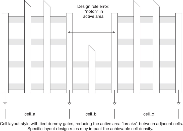
Figure 1.25 Illustration of a merged dummy gate layout style between adjacent library cells. A design rule error is introduced by the resulting notch in the merged active area.
Adjacent cells may result in a “notch” in the active area that violates process lithography design rules. The methodology flows to support (limited) abutment of the active area in different cells require additional consideration for cell characterization and IP block physical layout completion.
Much as with FD-SOI, the FinFET process does not easily provide for a (high-quality, vertical) p-n junction or bipolar transistor. Analog IP design requires adaptation to the available circuit elements.
1.4.7 Operating Corners and Modes
Logic path timing closure, power dissipation calculations, and electrical analysis all need to be confirmed over the full range of fabrication process variation, temperature extremes, and operating voltages. Specifically, there are local and global variations to factor into the analysis. The supply voltage applied at the chip pads minus the power distribution network voltage drop margin is used to assign the local circuit voltage. A chip thermal map helps determine the local rise in temperature above the ambient environment. In addition, there are tighter process variations locally than would be measured globally across the die or wafer or fabrication lot; in this case, the “tracking” of local circuits helps reduce the range of electrical and dimensional parameter variations to consider.
The evaluation of timing, power, and electrical characteristics across the full extent of process, voltage, and temperature (PVT) ranges is impractical. Rather, a set of PVT corners is defined for analysis. For example, an “sslh” corner would imply that circuit analysis was conducted using a “slow” nFET, “slow” pFET, low applied VDD at the chip pads (minus the PDN voltage drop margin), and high temperature. This corner would typically result in the slowest circuit delays for path timing and the data setup-to-clock timing checks at flip-flop inputs. Conversely, the “ffhl” corner-based timing delays would be used for data hold-to-clock path timing checks.
Product marketing may include performance sorting, or “binning,” of parts based upon their measured performance; higher-performance parts from the statistical fabrication distribution might command a premium price. To assist with the estimation of the fab yield by bin, it is common to add a nominal, or “typical,” transistor model corner for analysis. The “ttlh” corner reflects a nominal fabrication process, with the voltage and temperature extremes to which the part will be subjected in the final product application.
Although the highest operating temperature has typically been associated with the slowest circuit performance, due to both device current characteristics and interconnect resistance effects, that assumption is no longer neessarily valid. The device current is a complex function of two temperature-dependent parameters: the threshold voltage (Vt) and the inverted channel carrier mobility. The device |Vt| and carrier mobility both decrease with increased temperature; the decrease in |Vt| provides greater device current, while the decrease in mobility reduces device current. At older process nodes, the mobility reduction was dominant, and device current decreased at higher temperature. At newer nodes, the scaling of the nominal device Vt (commensurate with the reduced VDD supply voltage) results in a more complex interaction between threshold voltage and mobility. As a result, the high temperature corner may indeed result in greater device current, a phenomenon known as temperature inversion. However, interconnect resistance still increases with temperature, further complicating the electrical behavior.
The process variation ranges are applicable not only to the transistor characteristics but also to the tolerances on the fabrication of interconnects and vias. The use of chemical-mechanical polishing (CMP) for wafer planarization after damascene metal deposition results in wire thickness variations. The use of multipatterned decomposition and multiple lithography/etch process steps for interconnect shapes on a single layer will result in tolerances in the distance between adjacent wires due to mask-to-mask alignment variation. As a result of CMP-based and MP-based process steps, there will be ranges of interconnect resistance and wire sidewall-to-sidewall coupling capacitance. The definition of an analysis corner thus needs to be expanded to include variations in the extracted interconnect parasitics. For example, the additional parasitic calculations could include min/max C_total, min/max R*C_total, and min/max C_coupling. As with the temperature inversion behavior, it is not necessarily definitive that a specific corner is always the worst case or the best case for path timing checks and electrical analysis.
In short, multiple PVT corners need to be evaluated across all methodology flows. EDA tool vendors have adapted their algorithms and data structures to support concurrent, multi-corner analysis on the network of devices and interconnect parasitics.
In addition, the SoC design likely has multiple logical operating modes, each with corresponding power/performance requirements. For example, there may be design states that include:
Performance boost—Technically, a new PVT corner, with a higher applied supply voltage to support higher clock frequencies
Sleep mode—Inactive clocks and perhaps a reduced supply voltage with logic state and memory array values “retained”
Deep sleep—Supply or ground rails isolated from logic networks using series “off” sleep devices, with the lowest leakage currents, as depicted in Figure 1.26
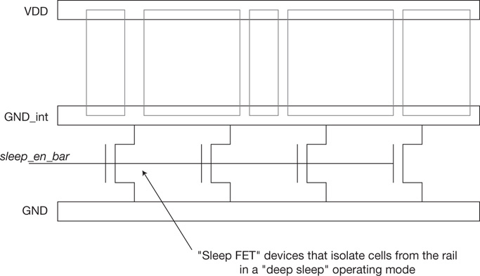
Figure 1.26 Circuit topology for a deep sleep operating mode, with the addition of sleepFET devices between an internal rail and a global rail. nFET sleep devices and a split GND distribution are shown.
Test modes—For example, serial scan shifting of test pattern stimulus and response data, at a reduced test clock frequency
It is therefore necessary to create a “cross-product” of operating modes and corners to analyze. EDA tools have been expanded to accept definitions of different modes to sensitize the related logic paths; a concurrent multi-corner, multi-mode (MCMM) analysis is then performed.
The SoC methodology and design teams need to review the mode-corner matrix to determine the necessary conditions for each analysis flow step. Some combinations can be excluded for a particular flow. For example, test mode operation would not be applicable to a performance boost voltage corner. (The various sleep modes require unique analysis flows, to be discussed shortly.) Nevertheless, the number of MCMM combinations can be large; the computational workload to run MCMM analysis on the full-chip SoC model would be prohibitive. The methodology needs to evaluate IP blocks efficiently over the MCMM matrix and provide appropriate abstract models for full-chip analysis. For IP received from an external supplier, these abstracts are a key deliverable, spanning the corresponding modes and corners for the final SoC application.
There is an additional methodology consideration related to special analysis requirements for mode state transitions. For example, an IP core transition from a deep sleep state to an active state results in unique circuit current distributions. During the deep sleep duration, network nodes are disconnected from one of the rails; thus, these floating nodes drift over time to an unknown voltage level due to various leakage currents. At the transition back to an active state with the network reconnected to the rails, there are significant rail currents to charge/discharge the internal network nodes. Commonly, the resistance of the logic network to global rail connection is gradually reduced during this mode transition, through the turning on of successive sleep devices in parallel over multiple “wake-up” clock cycles. The rail in-rush current needs to be analyzed over the allocated number of clock cycles to ensure that rail peak current values are within appropriate limits. (SoC functional validation also needs to ensure that the clock cycles are logically allocated to this transition and that logic functionality is not assumed before the wake-up transition is complete.) Once active, electrical analysis is required for the effective “on” resistance of the parallel sleep devices to ensure that the active network current does not adversely impact I*R voltage drop margins. The methodology needs to ensure that flows cover the unique requirements of mode transitions in addition to the MCMM tool capabilities.
1.4.8 Process Variation–Aware Design
The previous section describes how the expected range of process and environment variation is represented by analysis corners. When the set of process parameters is selected for a corner, there is an implicit assumption on the statistical distribution of the corresponding circuit delay. For example, if the circuit delay is measured repeatedly by sampling across all process parameter variations, a composite normal (Gaussian) distribution would result. The target best-case (BC) or worst-case (WC) process variation is a specific number of standard deviations from the nominal, mean performance – e.g., a “three-sigma” delay. Path timing closure and electrical analysis using the corner parameters will effectively represent an n-sigma point on the overall performance/power distribution, as depicted in Figure 1.27.
Figure 1.27 The process parameter set selected for a (worst-case or best-case) PVT corner represents a composite of many individual parameter variations to provide an effective n-sigma circuit delay.
Note that at advanced process nodes with aggressive VDD supply voltage scaling, the statistical delay distribution results for a characterized logic circuit across process variations is decidedly non-Gaussian; in this case, a different method to define process corner definitions is required.
For more accurate variation analysis, an extended approach is warranted. Superimposed on the overall global process distribution is a local distribution. Circuits that rely upon matching characteristics for device pairs need to perform offset analysis, using assumptions on local device variation. Similarly, interconnect R*C parasitics have on-chip variation (OCV), which is an important consideration for calculating clock skew and signal data path-versus-clock arrival timing tests at sequential circuit inputs. A modified global corner parameter definition is used as a starting point; a local distribution is added, and its standard deviation increases with the distance between which circuits are placed on the die. The endpoints of the local distribution provide a new parameter set that can be applied to individual instances in analysis flows to model OCV extremes. Alternatively, multiple analysis simulations can be performed by repetitive (Monte Carlo) statistical sampling from the local distribution. The results data from multiple simulation iterations provide an analysis output distribution for further yield review.
The complexity of timing path networks is very high: Rather than use a statistical sampling method for entire paths, a unique approach to modeling OCV for timing analysis is commonly used instead, applying derating multipliers to the delay arcs in each path (see Section 11.4).
Variation-Aware Array Design
Large memory array IP presents a unique consideration for variation analysis. The sheer number of devices in the array suggests that a much higher-sigma set of analysis parameters should be used. Three-sigma circuit-limited yield (CLY) design closure on a large array would imply a potentially significant number of marginal “weak bit” cells and, thus, a larger allocation of spare array rows/columns to maintain sufficient fabrication yield. The goal to operate large arrays on a VDD_min supply voltage domain to reduce leakage power only amplifies the requirement to ensure that very few fabricated weak bit cells are present. Rather than use a 3-sigma CLY corner definition, array performance verification over process variation requires a statistical confidence analysis to a sigma value commensurate with the acceptable weak bit probability.
Array circuit simulations employ a high-sigma method to ensure valid read/write operation over the process variation distribution. Demonstration of array functionality to 5-sigma or 6-sigma yield involves sampling the parameter distributions, simulating the array operation, and measuring the results. The most direct circuit sampling approach employs a random Monte Carlo selection of parameter values; however, the number of simulations required to compile sufficient results data to demonstrate high-sigma yield would be prohibitive. EDA vendors have developed unique products for high-sigma circuit simulation. At a minimum, this simulation requires a full bit array column and sense amplifier network. Designers specify the measurement criteria that define a successful operation—for example, a written array value reaching x% of its final circuit node voltage by the end of the operation cycle or a sufficient sense amplifier bit line differential at the end of an array read. The EDA tool algorithm selects a sequence of parameter samples that efficiently explore the extremes of the results distribution for the measurement criteria. An n-sigma yield (with statistical confidence limits) can be calculated with far fewer simulations than a brute-force Monte Carlo sampling distribution would require.
High-sigma simulation with advanced sampling for array weak bit evaluation can be extended to other IP circuit types. For example, the capture of asynchronous data by a clocked flip-flop requires detailed characterization to analyze the probabilistic risk of the synchronizer entering a metastability fail condition. This synchronizer flip-flop characterization also benefits from a high-sigma simulation approach. (Note that the confidence level for a high-sigma sampled simulation is only as good as the accuracy of the parasitic extracted network surrounding the devices. Chapter 10, “Layout Parasitic Extraction and Electrical Modeling,” discusses some of the extraction accuracy, capacity, and runtime trade-offs.)
High-Sigma Simulation Fails
The methodology for high-sigma analysis is an adjunct to the conventional CLY corner-based IP characterization methods. IP library developers need to make this EDA tool investment to accompany their existing simulation flow. Of specific interest are the sampled parameters for any simulation testcases that fail the measurement criteria. An IP developer compiles a results summary for failing simulations to review with the foundry. The foundry’s continuous improvement process engineering team benefits from awareness of the critical process parameters, for which critical IP has a high CLY sensitivity. The foundry team can then focus on steps to reduce the variation of these key parameters.
Note that circuit-limited yield is a metric that is a function of IP design and fabrication parameter variation. CLY is distinct from the defect density-limited yield, which is a function of the manufacturing defects (per square millimeter of a specific size or larger) and the critical area of the SoC physical design sensitive to the presence of the defect. The overall fabrication yield is a product of these two factors; ideally, by design, the impact of the defect-limited yield is much larger than that of the circuit-limited yield.
1.4.9 Process Retargeting and Process Migration
The discussion on VLSI technologies in Section 1.4.1 indicates that direct lithographic scaling of physical layout to a new node or to an alternative foundry process at the same node was relatively straightforward through (roughly) the 130nm generation. EDA tool vendors offered layout migration and “layout compaction” tools to facilitate the retargeting of a design and automatic fixing of any (minor) layout design rule errors for the new process implementation. The diversity among different foundry PDK rules at more advanced nodes has increased, and the design rules between nodes at a specific foundry no longer broadly follow a predominant scaling factor. The introduction of multipatterning mask layers and the transition from planar to FinFET devices further complicate the migration of physical layouts. As a result, the recent usage of compaction tools has diminished.
To facilitate the efficient retargeting of layout designs, alternative approaches have emerged. For IP circuit design migration, EDA tool vendors provide parameterized layout cells and relative cell positioning, as described in the following sections.
Parameterized Layout Cells (pCells)
The circuit schematic includes transistor instances that correspond to parameterized layout cells, commonly known as pCells. Invoking the pCell software function generates a transistor layout that corresponds directly to the schematic parameters (e.g., W (or Nfins), L, N_fingers). The pCell function may also add the source/drain/gate contacts and local metal interconnects; this is a key advantage of invoking pCells rather than attempting layout migration, as the rules for these connections vary widely between process nodes and foundries. The “generate-from-schematic” feature in the EDA tool platform exercises the pCells and seeds the new physical cell layout with the individual transistors.
The relative positioning of the seeded pCell layouts can follow the positioning of the schematic drawing itself or utilize a preferred pattern selected from an existing pattern library. (For analog IP with critical device matching requirements, individual fingers of separate devices can use an interdigitated common centroid pattern to minimize process variation sensitivity.) The generated layout data retains the schematic connectivity between devices. The generated parameterized layout cells can be repositioned, and common schematic nodes can be merged in the layout, based on the underlying connectivity model. The parameterized cell function includes the layout updates to share a source/drain node with an adjacent device. Alignment of nFET and pFET devices (horizontally) enables the common gate input to be extended (vertically) to connect both. After pCell positioning and merging, a device-level router can be invoked to complete the IP layout to the schematic connectivity. (Additional parameterized code is invoked to add the necessary dummy shapes around the devices.) Although more complex than automated layout compaction, custom layout assist tools provide considerable productivity to generate and complete a correct layout from a (migrated) schematic.
Relative Cell Positioning
To facilitate efficient IP core-level layout retargeting, EDA tool vendors offer an algorithm to maintain the timing optimization characteristics of the core. Starting with an existing cell-level netlist and a physical implementation, a relative layout cell position description can be derived. This description can then be applied during placement with the retargeted cell library to retain an optimized topology. (If the retargeted library does not have a corresponding logic function for all the instances in the original netlist, a cell-to-cell remapping tool can be used.) A set of net routing priority constraints ensures that critical routes and the relative cell placement retain the focus on the timing-optimized paths from the starting design. After layout retargeting, the path timing and electrical analysis flows are exercised using the new process technology PDK.
1.4.10 Chip-Package Co-Design
The focus of this text is on the methodology and flow steps for VLSI SoC designs. However, a comparable methodology and development engineering investment is made for package substrate design and analysis.
The package design rules and package composite layer stackup technology files define the physical layout and electrical analysis characteristics, similar to the PDK data from the silicon foundry. EDA tools specific to package physical design import the stackup and electrical materials data, the chip pad image, and the corresponding package pin data. A combination of automated route and interactive layout features completes the chip-package connectivity. The package netlist is likely to also include additional (surface-mount technology [SMT]) components to be integrated with the SoC die (e.g., SMT decoupling capacitors). The package layout tool also applies designer-provided rule checks to maintain matching topologies for critical busses and differential signal pairs. Shielding constraints can also be applied to ensure signal routes are located adjacent to power/ground wires and/or between supply planes in the package cross-section, to minimize switching noise on the signal. Specific package layer via definitions are often used to maintain an electrical impedance for (high-speed) signal transmission to minimize discontinuity reflections.
Due to the unique (and more interactive) requirements of package design, the EDA tools used are distinct from the physical design tools for SoCs. As a result, there is an important “chip-package co-design” interface required to/from the SoC methodology flows.
Early Chip-Package Floorplanning
With VLSI scaling, the number of SoC I/O signals and supply voltage power domains has increased tremendously. Compared to the initial LSI packages using wire bonds from the chip pads to a lead frame prior to encapsulation, current VLSI SoCs predominantly use a flip-chip face-down die orientation, with a raised metal “bump” for chip pad-to-package substrate lead attach on a very aggressive pad pitch. This has enabled both the SoC signal I/O count to grow and the allocation of bump pads internal to the die to connect package supply planes directly to the power distribution networks on the top redistribution metal layers of the SoC metallization stack.
To ensure optimum package pin assignment, the initial chip-package co-design activity is to floorplan the chip signal pad locations and the corresponding package pins to evaluate the package signal trace lengths and trace congestion (see Figure 1.28).

Figure 1.28 Illustration of SoC die pad-to-package pin “flightlines,” providing visual feedback during package floorplanning to guide physical location assignments for the die and package.
At this point, no detailed package routes are available; a visual flightline view is typically sufficient to identify opportunities for improved SoC bump pad assignments and, ultimately, corresponding SoC IP placements on the chip floorplan.
As the package design flow is separate, an efficient exchange of bump pad coordinate and signal assignment to/from the package design toolset is an additional required SoC methodology flow step. For a flip-chip bump SoC attach technology, note that the SoC coordinates used by the package reflect the face-down die orientation. (The author is aware of a catastrophic impact to a chip design project where the “face-up” bump coordinates were used for the chip-package model exchange, and this went undetected until after assembly of packaged prototype parts.)
Chip-Package Model Analysis
Additional model exchanges between package and SoC domains are required for electrical and thermal analysis, as well.
For thermal analysis, a chip “power map” abstract is promoted to the package model. The (local) dissipated SoC power generates thermal energy that flows through both the die substrate and the die surface metal interconnects. A typical cross-section of a flip-chip implementation is shown in Figure 1.29, with an additional thermal interface material (TIM) layer compressed between die and package.

Figure 1.29 Die-package cross-section, illustrating the addition of a TIM layer for improved thermal conductance. Different thermal expansion coefficients result in mechanical stress across the interfaces between the underfill and die attach materials.
The thermal resistance of this model is used to determine the heat flux to the ambient. The product designer integrating the SoC subsequently uses the results of the package thermal analysis to confirm the suitability of heat removal in the product enclosure.
The heat flow through the die surface (and resulting thermal model solution) introduces another analysis requirement. The different interconnect and dielectric materials present in the redistribution metals, bumps, underfill, and package substrate have different thermal expansion coefficients. A mechanical stress is present across these material interfaces, which requires “stress fatigue” analysis to ensure reliability across an appropriate number of power on/off thermal cycles.
The chip power model abstract also needs to contain sufficient detail to represent the time-averaged and transient current through the power and ground bumps. The SoC simulation methodology captures this data from on-chip power distribution network I*R voltage drop analysis and adds to the power abstract. A package analysis flow uses the bump currents from the SoC abstract to simulate and verify that the supply/ground voltage transients are within the allocated design margins that were used when characterizing IP circuit delays. The package simulation model should include the extracted parasitic inductance of the package power network, as well as explicit decoupling capacitors.
To date, there is no industry standard for the chip power abstract model used by package analysis tools. The SoC methodology team needs to collaborate with the package design team to determine what data format is required by their flows and derive the power abstract from SoC-level PDN analysis methods.
Chip Electrical Analysis with Package Models
High-speed I/O interfaces require frequency-dependent circuit simulations to confirm that the signal losses between drivers and receivers are sufficiently managed to maintain voltage levels that are accurately interpreted at the receiver. For serial interfaces with source-synchronous clocking, the high-frequency losses and adjacent signal crosstalk result in increased inter-symbol interference (ISI) between unit time intervals, impacting the accuracy of data recovery. The package team needs to provide extracted parasitic networks for (sets of) chip interface signals to enable the SoC I/O designer to confirm proper electrical driver/receiver behavior. The package signal models are often provided as a multi-port S-parameter matrix to represent the frequency-dependent insertion, reflection, and crosstalk losses of the package. The SoC designer also includes a reference load model for printed circuit board losses connected to the package model to complete the network description from driver to receiver—part of an overall chip-package-system (CPS) simulation methodology.
The other main chip-package co-design interaction for the SoC designer is the flow for electrical analysis of simultaneous switching outputs (SSO), as depicted in Figure 1.30 (see also Section 14.3).

Figure 1.30 Simulation model to evaluate simultaneous switching outputs (SSO) signal noise propagation, including both the local VDD_IO and GND_IO distribution and package electrical models.
A set of chip pad drivers that may switch in unison in a narrow time window will result in a transient current spike through the local PDN. The SoC methodology flow for SSO analysis requires excising of parasitics from the package PDN model, addition of a reference load, and attachment of the SSO pad driver circuits and related on-chip VDD_IO and GND_IO networks for circuit simulation. Potential SSO issues to investigate are:
The magnitude of the transient I*R and inductive noise on the VDD_IO and GND_IO rails—The delay of the drivers is adversely impacted by excessive noise on the rails. As a result of noise on the VDD_IO and GND_IO supply rails, receivers are subject to changes in the input voltages that are adequately interpreted as the different logic levels (e.g., VIH, VIL). Quiet drivers on the same VDD_IO and GND_IO supply network propagate the PDN noise through to their pad outputs, as well.
“Overshoot” and “undershoot” on rails significantly beyond VDD_IO and GND_IO—Inductive “ringing” di/dt voltage transients beyond the rail values forward bias p-n junctions connected to the rails, injecting current into the substrate/wells. To reduce the risk of latchup, pad drivers commonly include additional injected charge collection “guard rings” to suppress any p-n-p-n triggering current.
Excessive fast/slow output signal slew rates—The I/O driver specification to the system designer needs to include min/max signal slew rates into the reference load; these slews are to be valid across the range of PVT corner simulations, which is a difficult design objective. I/O driver cells may include a set of PVT “compensation” inputs, which adaptively control the number of transistor fingers switched on in parallel (see Figure 1.31).
Figure 1.31 Schematic for adaptive control of pad driver output impedance. The number of active transistor fingers in the driver is dynamically varied, based on input from a PVT sensing circuit.
If compensated drivers are to be used, the methodology flow needs to verify the correct connectivity of the drivers to the PVT sense macro outputs and include the full (compensated) network in SSO simulations.
Chip-package co-design optimization requires that the SoC methodology export pad geometry data and electrical power abstracts to EDA tools outside the conventional SoC flows. Similarly, the methodology needs to import (excised) parasitic models from the package extraction tools for a variety of circuit simulation tasks. Due to the unique package design tools and (nonstandard) model formats that may need to be exchanged, special consideration should be given to additional model validity checking in these flows. An example would be to verify that an S-parameter model for package parasitics used for I/O signal simulation is indeed fully passive. As networks for circuit simulation are merged using chip and package parasitic elements, additional checks for dangling nodes are appropriate. The complexity of chip-package flow development is further expanded by the need to ultimately perform chip-package-system analysis using actual system model data in lieu of supply voltage drop margins and reference load models.
The discussion in this section on package analysis assumes a relatively straightforward single-chip module, with a multi-layer package substrate for signal and power plane distribution. There are an ever-increasing variety of multi-chip module (MCM) package technologies available, providing higher signal density and improved performance for inter-chip interfaces contained within the MCM. These advanced packages offer the capabilities of placing multiple dies adjacent to each other with connectivity through substrate layers or multiple dies stacked vertically using additional connectivity through an interposer separating the dies. The same chip-package co-design considerations discussed in this section extend to these MCM technologies (i.e., collaboration on floorplanning of chip pads and package substrate/interposer routes, utilization of chip power abstracts for package electrical and mechanical analysis, merging of package parasitics for I/O interface signal quality and SSO simulations).
1.4.11 Chip Thermal Management and Designing for a Power-Performance Envelope
For many high-performance SoC designs, there is an opportunity to boost the performance of the design if it can be ascertained that the (local) operating temperature is far from the extremes used for PVT corner circuit delay characterization. Conversely, it may be necessary to throttle performance if the operating temperature approaches the corner value. An SoC architecture may choose to employ a dynamic voltage, frequency scaling (DVFS) approach, in which a power management control module can vary the IP core supply voltage (and clock source frequency) corresponding to operating environment feedback.
Initial DVFS implementations added an external programmable power management integrated circuit (PMIC) to set supply voltages, typically communicating with the SoC through an I2C bus interface. More recently, an increasing number of SoC designs are using an integrated voltage regulator as part of the on-chip power management strategy. The integrated regulator offers faster response time (lower latency) for power state transitions, improved regulator input noise filtering/rejection, and extendibility to multiple core voltage domains, all with higher power efficiency.
Temperature Sensing
The on-chip power management design utilizes a temperature sensor IP macro from the circuit library. A variety of thermsense circuit implementations are employed, and their outputs are a function of temperature. Examples of thermsense macros include:
Bandgap voltage reference generator—The voltage difference between active junctions operating at different currents is (linearly) temperature dependent. The bandgap would be connected to an analog-to-digital converter (ADC) to provide a digital code for the measured temperature that can be readily routed to a power controller.
Sub-threshold current sensor—This sensor uses a similar topology as the p-n junction bandgap, using the difference in Vgs between two devices of different size operating in the sub-threshold current region.[15]
Ring-oscillator frequency variation—A ring oscillator feeds a reference counter to directly encode the temperature digitally.
The architecture for on-chip power management includes the thermsense macros, a power state controller, and programmable voltage regulators and clock generators, as illustrated in Figure 1.32.
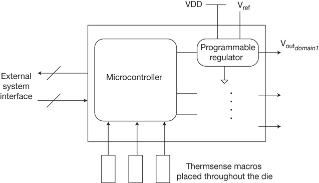
Figure 1.32 A representative block diagram for the on-chip power management architecture.
The microcontroller may also interface with the operating system to communicate environmental conditions and receive instructions for external control of boost/throttle/sleep states.
The methodology for adding power/performance management on-chip starts with a review of the IP library offerings for the voltage regulator and thermsense functions. The specifications for this IP need to be reviewed against the SoC requirements for DVFS operation:
Temperature range and temperature reporting tolerance (over process variations)
Reference voltage input(s) required to the regulator
Regulator programmability
Regulator output voltage characteristics, as a function of current load (and dynamic load variation), and additional recommended capacitive filtering
Latency for boost/throttle transitions
Robustness of regulator output voltage behavior during a DVFS transition
An SoC incorporating temperature-based boost/throttle support introduces new methodology flow constraints:
Circuit delay/power dissipation characterization needs to be extended to the boost voltage.
Electrical analysis corners need to likewise reflect the extended boost operating range.
Specifically, noise coupling between nets is impacted by the voltage transition signal slew, which is faster as a result of applying the higher boost voltage. Electromigration current density is also impacted.
Additional macro usage checks should be employed to confirm that the thermsense macro is correctly inserted and connected to the power management module inputs. In other words, the thermsense macros and voltage regulators become an integral part of the functional validation of the power state microcontroller. The thermsense macros do not have a digital model, so they are “stubbed out” during functional model compile and elaboration. Their inputs and outputs become response and stimulus points in the testcases exercising the power controller. For SoC physical implementation, the placement of the temperature sensors requires consideration of the anticipated hot spot locations. The routing of the thermsense outputs and power management controls requires an allocation of (global) wiring track resources.
Chip Thermal Management
The SoC power management architecture also introduces new production test considerations. For efficiency, a selected subset of boost/throttle conditions could be examined for delay-based test patterns by sending specific codes from the controller to the voltage regulators and clock generators, bypassing the thermsense outputs. The capability to set IP cores to a lower power dissipation (inactive) state could be employed during production test as well. Rather than requiring full active power delivery through the test probe fixture, a production test could use a sequence of power state transitions and core-specific patterns. This would be particularly attractive during burn-in stress test screening, in which multiple packaged parts are socket-mounted in parallel on a burn-in board. Although the pattern test time would be longer, more parts could be stressed in parallel within the power supply delivery and thermal constraints of the burn-in chamber.
The logical, physical, and test requirements for the thermsense and regulator models suggest that they are directly included in the core hierarchy; it would be more difficult to represent them as separate global instances in the SoC hierarchy.
In addition to the functional validation of the interface between the power controller and thermsense and regulator macros, there is a complex set of power state transition testcases. Cell usage checks are required to confirm correct instantiation of level-shifter circuits and state retention flops. Logic inserted to block undefined signal propagation at the interfaces between cores at sleep and active states also needs to be verified. To facilitate the efficient application of these cell usage checks and the (automated) generation of functional validation testcases, EDA vendors have enabled SoC methodology flows to incorporate a concise power intent specification file (see Section 7.6).
1.5 Power and Clock Domains On-chip
The previous section introduces some of the design considerations for incorporating multiple SoC power supply domains. This brief section highlights the interface requirements between power domains. The interface between clock domains also introduces specific clock usage and checking requirements.
1.5.1 Power Domain Constraints
Methodology flows are added to check valid and required cell usage at the interfaces between distinct power domains on the SoC. As mentioned previously, a power format file is a separate functional description that is used to identify the specific interfaces in the SoC hierarchy, where EDA tools apply the necessary library cell checks. Separately, EDA vendors have developed tools to assist with identification of clock domain crossing paths and implement the appropriate cell checks.
A level-shifter cell accepts an input logic signal at a logic ‘1’ voltage level below the VDD supply voltage of the receiving domain, as illustrated in Figure 1.33. It is required at interfaces when the sourcing domain operates at a lower supply voltage.
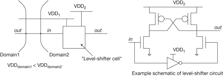
Figure 1.33 A level-shifter cell adapts the logic ‘1’ voltage level from a sourcing block to the (higher) supply voltage of the receiving power domain. Note that both supply voltages are required to the level-shifter cell, necessitating a more detailed power distribution. Typically, the level-shifter cell is located within the higher VDD domain.
If a core enters a full-sleep power state—either by the disabling of series sleepFET devices or by being controlled by a voltage regulator—the output signal values of the domain reach an unknown voltage and thus become logically undefined (see Figure 1.34).
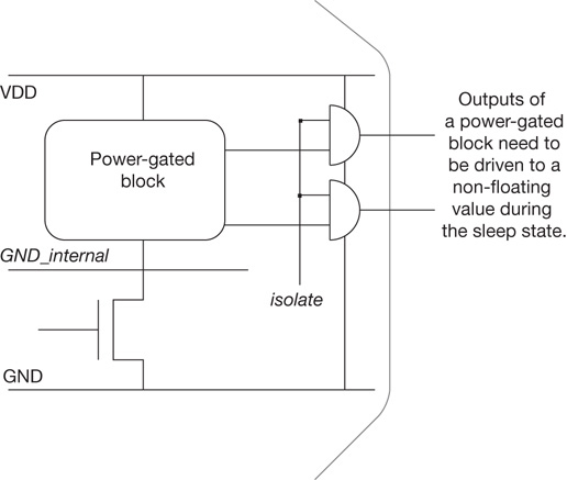
Figure 1.34 Isolation cells are added at the outputs of a power domain to provide fixed logic signal values to fan-outs when the domain is power gated. Note that the isolation cells connect to the non-gated rails within the domain to always remain powered.
It is necessary to block these undefined logical (and signal voltage) levels from propagating into active domains. Usage checks are needed to confirm correct interface behavior.
If a core enters a full sleep condition, by default all internal logic state values are also lost. In order to minimize the time required to recover from the sleep condition, special state value retention flop library cells can be employed. These cells necessitate using a cell template that includes access to the active supply rail during the sleep state, as shown in Figure 1.35.

Figure 1.35 State-retention flop cell to retain internal state values when a block is power gated and restore state when the block returns to active operation.
The functional validation team needs to confirm the sequencing of the “retain” signal to save the flop state prior to the sleep transition and restore the value as part of the transition to the active power mode.
1.5.2 Clock Gating
An efficient method of (active) power reduction within a domain is to implement clock gating. If it can be logically determined that the logic state values of a network are valid for one or more future clock cycles, the clock input transitions to registers can be suppressed, saving the power associated with the clock pin loading and any logic switching activity not influencing the network state. Figure 1.36 shows a rudimentary example in which a free-running clock to a register is converted to a gated clock, in the case where the register values would be unchanged.

Figure 1.36 Clock gating logic implementations. To simplify enable input timing constraints and ensure that no spurious clock pulses propagate, an integrated latch is typically used, denoted as an ICG cell.
Note that the clock gating library cell has special design requirements. To maintain the fidelity of the clock pulses and minimize skew, the clock gate needs delay characteristics comparable to those of the clock buffer being replaced. Also note that there are strict constraints on the clock gate enable timing. There must not be any spurious (or short, truncated) clock pulses due to enable signal transitions while the clock phase is active. A common clock gate implementation inserts a latch between the enable signal and the clock gate, where the latch blocks enable transitions on the active clock phase. There is a setup time constraint at the clock gate for the enable signal, as well. The specific clock gating cells in the IP library include timing constraints so that the required path timing tests at their (combinational) gate pins are enforced during the timing analysis flow.
The combinational clock gating topology reduces wasted power associated with a static network state. Greater savings are achievable with sequential gating, as illustrated in Figure 1.37.
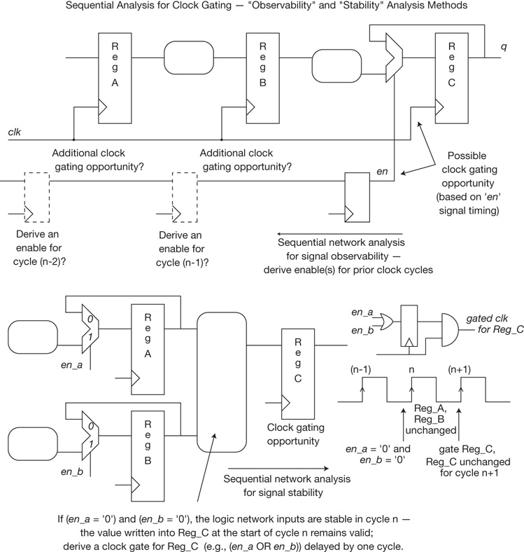
Figure 1.37 Illustration of sequential clock gating logic. Both sequential signal observability and sequential signal stability examples are depicted.
EDA vendors have developed tools to evaluate hardware description language designs and identify potential combinational/sequential gated clock enable expressions and the corresponding logic design transformations. If these clock gating tools are employed, the SoC methodology team needs to confirm that the functional equivalency flow is capable of (independently) proving that the new gating model is logically identical to the original, before accepting the transformation.
1.5.3 Clock Domains
The clock domains on an SoC are interdependent with the design hierarchy. For a hierarchical interface between timing models in the same clock domain, a set of timing constraints relative to the common clock needs to be maintained. Figure 1.38 depicts an elementary example.

Figure 1.38 Examples of timing constraints to be provided for block-level analysis, relative to a common clock reference; timing paths are launched and captured at state elements. Constraints are required for each PVT corner used for timing analysis.
To enable path timing analysis and optimization between the two models in the figure, designers need to specify constraints such as required_arrival_output_time_A, estimated C_load_A, min/max_signal_slew_A, expected_input_arrival_time_B, expected_C_in_B, and expected_input_slew_B. These timing constraints are relative to the common clock reference and are required for each timing corner. The path timing analysis methodology flow adds compensation for the potential clock arrival skew at the launch and capture state elements (see Section 11.3).
The data management tools in the SoC methodology are responsible for associating the constraints file with each model revision. In addition, the methodology should include checking utilities that aid designers, including the following:
The required output arrival times are always less than the expected input time on the net; in equation form, (RAT_A < EAT_B).
The Cload_A constraint is consistent with the sum of the fan-out input pin capacitance.
The output pin slew and input pin slew constraints are consistent (i.e., slew_A < slew_B).
Perhaps most importantly, from individual block-level path timing analysis results, the constraint checking utility could identify cases in which the positive and negative slacks for the output and input pin arrival times at the blocks need to be re-apportioned (or “re-budgeted”) across the interface.
Clock domain interface timing constraints enable designers to work independently on (partial) path optimization within their respective blocks. It is important to ensure that opportunities to accelerate closure on failing paths between blocks are identified and timing constraints adjusted accordingly.
In cases where the interface between blocks represents paths that are associated with unrelated clocks, a synchronization flop is required to capture the signal to the new clock reference, as shown in Figure 1.39.

Figure 1.39 A unique synchronization flop cell is required at clock domain crossing interface. The circuit design of this cell specifically focuses on reducing metastability output transition behavior.
The launch-to-capture path between two blocks utilizes unrelated clocks if there is no timing relationship between the two clocks and there is no corresponding expected arrival time at the receiving block pin. A specific IP library flop cell is provided for asynchronous interfaces. The circuit characteristics of this cell differ from more conventional flops. Synchronization requires reducing the probability that the flop will enter and linger in a metastability state due to the indeterminate data arrival-to-clock transition interval. Internal circuit node capacitances and feedback transistor drive strengths are optimized in the synchronizer to minimize the node transit time to a stable state. The metastability probability can be further reduced by placing multiple synchronization flops in series at the asynchronous input pin.
The SoC methodology flow needs to include two features specific to asynchronous clock domain interfaces:
Metastability failure rate calculations, which are a function of the input data rate, capture clock frequency, input signal slew, internal time constant of the synchronizer circuits, and flop output capacitive load
Checks that the synchronizer flop is present at the interface or multiple flops in series, based on the failure rate calculation
EDA vendors offer tools that identify asynchronous clock domain crossings in a hardware description language model, tagging signals with their sourcing clock and propagating through logic expressions to the capture clock. (Note that conventional hardware description language simulation is not designed to reflect the very low probability of asynchronous interface metastability issues.) The methodology flow utilizes the relationship between a signal and the sourcing clock for the synchronizer checks.
This discussion on clock domain interface design and constraint management has made a simplifying assumption of a single clock reference for sourcing signals and a single (perhaps asynchronous) clock reference for capturing logic path results. SoC designs commonly employ more complex clocking features, with the possibility of using divided functional clocks and/or multiplexed clocks within and between domains. The chip reset clocking and wake-from-sleep state also introduce special timing constraints. Another typical example is the addition of production test clocks within a domain to implement the logic for serial shift-register scan of test stimulus/response data (see Section 7.3) or the clocking of dedicated built-in self-test (BIST) logic networks (see Section 19.3).
The SoC methodology and design teams conduct a project kickoff review of the clocks used throughout, the MCMM modes for timing analysis (IP blocks and full chip), and the timing constraint hierarchical management. The outcome of this review defines the flow inputs required and the results data to be tracked by the methodology manager application (see Section 2.3).
1.6 Physical Design Planning
1.6.1 Floorplanning
The initial methodology step in SoC physical implementation is the positioning of IP blocks on the die image, commonly denoted as floorplanning. This flow often utilizes a combination of automated placement algorithms and (iterative and interactive) manual refinement, using specific features of EDA vendor layout editing tools.
Floorplanning involves many optimization decisions during IP block coordinate assignment within the die:
Hard IP will have a fixed extent and aspect ratio. The netlist for soft IP cores is not available for early floorplanning; cell count and corresponding area estimates are needed. Further, the aspect ratio of the area allocated to the soft IP is somewhat flexible. Note that a high aspect ratio for the estimated area may be useful to fit between other blocks but is likely to result in significant routing congestion within the core in the narrow dimension. Also, the soft IP area estimate should reflect an appropriate cell utilization percentage for internal routability and the addition of decoupling capacitance.
The horizontal and vertical dimensions of the IP core blocks need to reflect a multiple of the global wiring track grid. The origins of the blocks need to snap-to-grid for FinFET technologies.
The global routing requirements between IP are a crucial floorplanning consideration. Initially, the visual feedback in the floorplan layout editing tool highlights the flightlines between IP cores, based on the hierarchical top-level connectivity between blocks. (The origin and destination of the flightlines use the center of the block, prior to detailed pin assignment.) The density and length of the flightlines can indicate potential global route congestion issues, including the need for additional global signal buffering and/or sequential repeater flops. The floorplan tool may calculate additional data that are useful to IP placement optimization (e.g., a total global wire length estimate, a comparison of the number of flightlines crossing sections of a [coarse] grid to the number of wiring tracks associated with each grid segment). Any global wiring track blockages associated with hard IP placement need to be included in the flightline calculation.
The floorplanning tool allows the addition of a predefined global track allocation to critical busses; in this case, IP flightlines connect to these global tracks.
The floorplanning of SoC I/O pad arrays is a key element of chip-package co-design (see Section 1.4.8). The flightlines from internal IP to the pads are a critical part of the IP placement optimization.
Pin Assignment
Pin assignment is a key optimization phase as the floorplan begins to stabilize. For hard IP, the pin locations for each core input/output signal are fixed; nevertheless, there is likely an opportunity to flip/mirror the hard IP layout view to minimize global signal length and optimize performance. For example, many SoCs incorporate multiple instances of the same processor core, which communicate across a multi-point internal bus architecture; to optimize the core-to-bus interface performance, a hard IP instance is flipped so that pin locations are shortest to the global tracks allocated to the bus. For soft IP, there is more flexibility in pin assignment during floorplanning to address several constraints:
Pins need to be assigned to a specific metal layer, corresponding to the expected union between the global routes and the internal IP physical implementation.
Pins need to be located on a global wiring track. In addition, if the pin metal layer corresponds to a lithography layer that will be part of multipatterning decomposition, the pin may also need an assigned color.
The width of the pin may need to be larger than the minimum wire width of the metal layer. If the signal pin is part of a critical timing path, the global route (and internal IP metal to the pin) may use a non-default rule (NDR) as a routing constraint, as illustrated in Figure 1.40.

Figure 1.40 The pin shape for an IP block defines the width and metal layer for the global route. Based on the internal IP circuitry, wider (non-default) global wire connections may be required.
In a library cell layout, it is common to provide a physical pin shape that spans multiple wiring tracks to offer the router greater flexibility in completing local routes. The physical abstract of the cell has a pin property which indicates to the router that any valid track connection is acceptable. For an IP block model in a floorplan, the pin property (and global signal routing directive) typically requires full pin coverage. For example, the IP designer must make assumptions on the driver strength required to connect to global busses. The pin output drive strength determines the corresponding global signal wire width and, thus, the size of the pin shape in the IP block abstract used during floorplanning.
A routing rule assigned to a global signal may require wide interconnect segments for optimal performance. However, a fan-out of that signal may terminate on a narrow width IP input pin necessitating that the global route be tapered, as depicted in Figure 1.41. The methodology team needs to review the foundry PDK design rules for wire segment width tapering and ensure that the router will observe the NDR global route constraint up to the tapering distance.
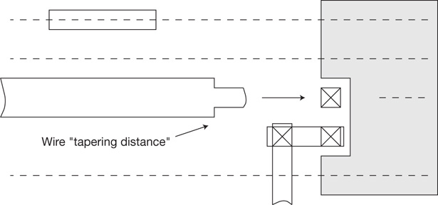
Figure 1.41 A global route may utilize a non-default wire width for performance, tapered at the IP pin shape; the metal layer design rules for tapered shapes need to be observed.
In addition to pin width selection, pin location assignment is also a complex optimization during soft IP block floorplanning. The goals of pin location assignment are varied:
Minimize the global wiring track demand.
Optimize performance for critical timing interfaces between IP blocks.
Avoid internal wiring congestion during subsequent IP block physical implementation.
Maintain the accuracy of the timing constraints and the IP timing abstract models used for path timing analysis.
The last goal introduces a physical design constraint. The block input pin data should be able to accurately reflect the capacitive loading within the block. As a result, the input pin should be physically close to the corresponding fan-out cells. It would be difficult to represent a long wire between pin and cells in the IP timing abstract for the calculation of the effective capacitance load on the driving circuit (see Section 11.1). Figure 1.42 illustrates the complexity of estimating the load at the block pin for the IP timing abstract for a long internal R*C wire.
For a hard IP layout, this physical constraint implies that pin locations internal to the IP boundary may be present. For soft IP, although internal area pins need to be supported by the methodology, it is much more common to assign pins to the edge of the IP physical boundary in the floorplan. The expectation is that the subsequent soft IP physical implementation will place cells logically connected to a pin with a strong affinity to the floorplan pin location.

Figure 1.42 A distributed RC parasitic from a block pin to internal fan-out is difficult to model as an effective capacitive load at the pin for the block abstract; pin-to-fan-out connections should be short.
An enhanced floorplanning (and soft IP block routing) tool feature would allow a pin to be included in a pin group, with the group assigned to a range of wiring tracks on the boundary edge, as illustrated in Figure 1.43. The pin group would allow some optimization flexibility during the detailed block routing flow yet still provide sufficiently accurate data for early IP floorplanning. The detailed pin assignment after routing needs to be reflected in a floorplan version update to complete the global routes.
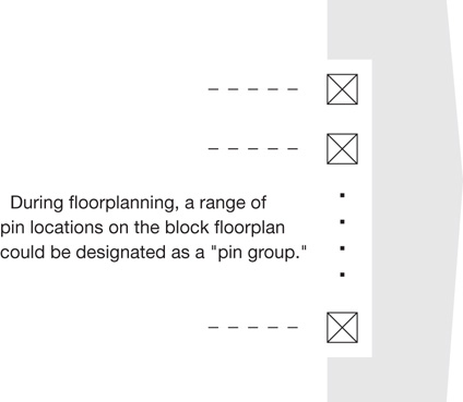
Figure 1.43 Soft IP block pins allocated to a range of floorplan wiring tracks during floorplanning, as part of a pin group.
The requirement for accuracy in the soft IP timing model also typically precludes the creation of multiple physical pins for a single logical output signal. Figure 1.44 illustrates the timing model inaccuracy associated with multiple block IP physical pins for a logical output.

Figure 1.44 Multiple block physical pins for a logical output are difficult to model accurately in a block timing abstract.
The initial “firm” SoC floorplan release allows IP designers to proceed with their physical block design and allows the physical SoC integration team to work on global signal buffer and repeater requirements. The floorplan needs to be maintained and updated, as SoC logic validation and production test development will inevitably result in changes to the IP block input/output signal interface list. The floorplan is the link between logical and physical hierarchical models; the version release management policy for logic models impacts the floorplan data, as well. The EDA floorplan tool needs to input the (revised) logical model, compare against the current physical design, and report/track any pin discrepancies. The SoC project management team must continually assess the stability of logic model revisions and decide when the connectivity of the logic model and of the physical floorplan need to be aligned and a new floorplan version released.
1.6.2 Power Grid and Wiring Track Planning
The quality of the SoC floorplan relies on a calculation of the available global wiring tracks, compared to estimates of the wiring segment demand across the chip. The global power grid definition subtracts from the available signal tracks and needs to be incorporated into the floorplan.
The global power grid is actually a set of separate grids for individual power domains. The floorplan designer needs to ensure that the power domain assumptions for each block are reflected in the placement of corresponding grids. The connectivity of the power grids to chip pads is also part of the floorplanning task (i.e., routing from pads/bumps—perhaps internal to the die area—through top-level redistribution metal to connect to power grid access points).
The term power grid is used somewhat loosely. If the foundry process supports the stacking of vias between successive metal layers, the actual PDN metal utilization may be rather sparse on (some of) the intermediate layers. The power grid points may consist of a sequence of via arrays and metal coverage shapes between upper and lower layers, as illustrated in Figure 1.45.

Figure 1.45 Illustration of a sparse global power grid, leveraging the availability of stacked via arrays between metal layers.
The via arrays provide a lower-resistance current path to the thicker top-level metals, at the expense of blocking multiple adjacent tracks for the covering metal. Nevertheless, compared to a denser grid of intermediate-layer metal segments, the sparse grid with stacked via arrays is likely more effective overall, both electrically and for signal wiring track layer availability. On the other hand, some signals may require that the router provide shielding (e.g., routing a signal in a track adjacent to a power/ground rail) to minimize capacitive coupling noise from neighboring wire switching transients. A denser PDN grid of metal segments throughout the metallization stack offers more opportunity for the router to assign these critical signals adjacent to the grid to serve as a shield. There are complex trade-offs to be considered when developing the PDN grid topology for a power domain.
A key parameter in the design of the grid is the estimated power dissipation of the corresponding domain. The number of chip pads and pad redistribution and the density of grid points are adapted to satisfy the power dissipation of the domain. For example, if the switching activity is low, via grid points could potentially be sparser; the electrical analysis of the local I*R voltage drop would provide closure on the suitability of the grid (see Chapter 14, “Power Rail Voltage Drop Analysis”).
The connectivity of the floorplan power grids to the SoC blocks (and global circuits) differs for hard IP and soft IP blocks:
A hard IP block includes an internal grid within the layout. The floorplan grid needs to cover the power pin shapes added to the IP physical model abstract. An analog hard IP block will likely require special focus on the power grid density for its power domain to minimize (static and dynamic) voltage drop.
The physical implementation of soft IP blocks is not available during initial floorplanning. Rather, the cell library template and local track definition include the local power grid; the floorplan grid aligns with the access points on the cell library template grid.
The floorplan power grid design may include a population of additional specific decoupling capacitance elements. The fabrication process typically provides the option of adding a thin intermediate metal layer, used to implement a metal-insulator-metal (MIM) structure. The MIM provides an area-efficient capacitance implemented within the upper-level metals, as illustrated in Figure 1.46. The power grid template now requires connection to the parallel plates of the MIM structure. (The intermediate metal layer is not a routing layer.) Note that the MIM decoupling element is electrically present between the local decap library cells interspersed with logic circuits and the SMT capacitors added to the package substrate.
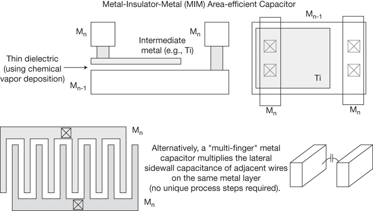
Figure 1.46 Cross-section of a metal-insulator-metal (MIM) capacitor structure residing among upper metals. The intermediate metal layer is provided by the foundry as a process option. The intermediate metal plate of the MIM is shaded in the figure. A thin dielectric is deposited over layer Mn-1 prior to patterning of the intermediate metal. This parallel plate capacitor is contacted on metal layer Mn in the power grid template. An alternative decoupling capacitor structure is also shown: interleaved multi-finger metal “combs” on metal layer Mn, where the sidewall capacitance between the fingers provides the decoupling.
The floorplan power grid for any cores implementing a DVFS or sleep state feature requires additional design considerations. If an integrated voltage regulator is employed on the SoC, the regulator power connections for Vin and Vout need special power grid design. If an IP block utilizes a sleepFET topology to turn off the core, a global power grid for VDD and VSS needs to align with the block VDD and VSS grid, plus the allocation of local rails consistent with the cell template for VDD_core (pFET sleep) or VSS_core (nFET sleep) distribution.
As the SoC floorplan evolves, the corresponding power domain grids need to track the changes. The floorplan methodology flow needs to confirm the correct grid overlay for each IP block, which satisfies any specific IP features, supports the power dissipation estimates, and enables accurate global wiring track resource calculations.
1.6.3 Global Route Planning
During initial floorplanning, the flightlines between IP cores highlight the global route demand. These flightlines ultimately need to be converted to a combination of horizontal and vertical segments, also known as a Manhattan routing style.
Note that early VLSI process nodes supported more general routing segment directions for global signals (e.g., allowing 45-degree segments to switch tracks on a single wiring layer). Commonly, non-orthogonal segments are now permitted only on the top redistribution layer. (There was a short-lived methodology effort with some EDA support to define global routing tracks with entire layers dedicated to a 45-degree orientation, with related vias to orthogonal metal tracks on layers above and below.)
As VLSI scaling has continued, the PDK lithography design rules have reduced the routing flexibility to preferred directions for alternating metal layers, with more conservative widths/spaces for any orthogonal wrong-way segments (routing track jogs) on the layer. When estimating the wire length between pins, the Manhattan distance is applied, with the assumption that the final detailed global route will not experience an excessive scenic path. For a multiple fan-out global signal, a Steiner tree topology estimate is used, as illustrated in Figure 1.47.
For performance-critical nets, the wire track demand calculation promotes segments to the thicker upper global layers in the metallization stack.
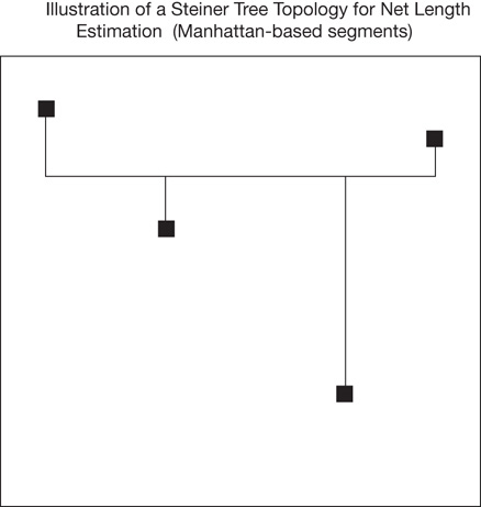
Figure 1.47 Interconnect estimates for Manhattan routing wiring layers typically utilize a Steiner tree topology.
The floorplan design may incorporate dedicated wiring tracks allocated to a signal bus, which directly provides a Steiner topology for wiring track estimation. The prerouted bus segments may be greater than minimum width for the assigned layer and/or may incorporate adjacent shields.
The IP cell library needs to include a specific set of buffers and sequential repeaters for global signals. The (Manhattan) wire length for global signals may necessitate inserting a buffer or repeater to improve path performance and avoid excessive signal slew rates. A preliminary simulation analysis of the global cells in the IP library with different loads should provide guidelines on the optimum segment length between inserted buffer or repeater cells, given the cell drive strength and global metal routing layer(s). Note that a floorplan designer has multiple options for the topology of a global signal, with the insertion of inverting and/or non-inverting cells.
If the global signal path (across a common clock domain) cannot satisfy timing constraints with the insertion of buffers, it is necessary to insert a sequential repeater flop cell. If a global sequential flop and/or aninverting buffer cell is inserted, the SoC top logic model needs to include the corresponding change in signal latency and/or polarity for logic simulation. (Of specific importance is the task to ensure that any separate high-level, C-language performance model of the SoC also reflects the additional interface latency due to the insertion of global sequential flops.) The completion of the initial chip integration project milestone requires updating the SoC logic model to reflect any global functionality introduced duringfloorplanning.
The space between IP block boundaries in the floorplan is called a channel. The inserted global cells assigned to a channel are grouped, and a small image of valid cell placement locations and power rails needs to be generated. The buffers and sequential repeaters are typically high-drive-strength cells; local decoupling capacitor cells should be included in the channel, as well. Some spacing between placed cells in the channel image may be beneficial, as the vias between the global signal upper metal layers and the cell input and output pins introduce wiring track blockages on intermediate layers.
When designing floorplan channels, the foundry requirements for insertion of layout cells used for process monitoring also need to be considered. For example, cells provided by the foundry to be inserted throughout the chip layout provide lithographic alignment measurement verniers. The floorplan also needs to allocate area for the insertion of identifying alphanumeric data, from the mask-layer nomenclature required by the foundry to the company part number and revision information. Individual die are lithographically stepped across the wafer, including a specific distance between die required for separation, denoted as the scribe channel. The floorplan includes the edge seal design around the top physical cell of the chip, a specific set of foundry layout design rules for all mask layers to provide a clean scribe break with minimal risk of layer delamination or die edge contamination.
1.6.4 Global and Local Clock Distribution and Skew Management
The SoC floorplanning design phase includes the placement of clock generation IP and the global distribution of clocks to their respective domains. A phased-lock loop (PLL) IP block is often used as the clock source; this circuit provides an internal clock that is a multiple of a reference clock input. (The supply power grid to this analog IP domain requires special design to minimize noise injection.) The clock distribution from this source to the SoC IP associated with the clock domain requires significant buffering and load balancing to minimize the arrival skew at each local IP clock pin input.
There are two prevalent global clock distribution styles: a grid and an H-tree. A global clock grid overlaps an IP core in a manner similar to a power grid. The global grid needs to cover all the IP clock input pins. This is a unique case, in which multiple physical input pins on an IP block correspond to the same logical input. For logic path timing analysis within the block, the model effectively collapses the multiple physical pins into a single source; an assumption is made about the clock arrival skews across the block. For flop setup timing analysis checks, this skew assumption is subtracted from the clock period; for “short path” flop hold timing, the assumed skew is added to the path delay between launch and capture endpoints. A separate methodology flow performs a high-accuracy parasitic extraction and PVT circuit simulation of the clock distribution to confirm the validity of the skew assumption (see Section 11.3). As with power grid distribution, the global clock grid is designed to provide a low-resistance path from the main clock driver to any point on the grid. Several advanced SoC flows have been developed to further tune the grid physical implementation once the detailed clock loading is known, such as tapering or truncating ineffective grid segments to reduce total clock dissipation power.
An H-tree is a network of symmetric segments at each level of a multi-stage tree, with buffers at the ends of the segments sourcing the next level, as shown in Figure 1.48.

Figure 1.48 Illustration of an H-tree clock distribution, with physical design optimizations to maintain low-skew arrivals and balanced cell delays at each level of the tree.
The H-tree relies on maintaining identical cell and R*C interconnect delays to the buffers at the next level. Note in the figure that the number of buffers increases at each level of the tree. The floorplanning of the H-tree is more complex than for a clock grid, as there are relatively strict requirements for the placement of the buffer cells and tree routes. Interfacing the buffers at the last level of the global H-tree distribution to the local clock inputs of the IP blocks also requires careful load balancing. On the other hand, the H-tree is likely to dissipate less total clock power than the global clock grid. In addition, it offers opportunities for clock gating earlier in the distribution if a buffer is replaced by a clock driver with a logic enable. A hybrid design implementation of a global clock H-tree and grid is also commonly used.
An additional design consideration for global clock distribution is the required shielding of clock signals by dedicating adjacent wiring tracks to a non-switching rail (perhaps at a relaxed spacing to the clock wire to reduce the total capacitance as well).
1.7 Summary
This introductory chapter has covered a broad set of material as background for more detailed discussions of specific methodology flows in subsequent chapters. A major point of emphasis in this chapter is the requisite methodology planning that is part of the initial SoC project definition. A methodology team must coordinate a wide range of SoC project characteristics, from high-level hierarchical data management and version control policies to detailed optimization decisions on foundry technology selection. The methodology team must also collaborate with a diverse set of engineering teams, both those that are directly involved in the SoC design (e.g., architects, logical and physical designers, test engineers, project managers) and teams that support the SoC design. Specifically, the methodology team maintains a close working relationship with three support teams: (a) the engineering team working with the foundry and OSAT for technology support, (b) the engineering team working to qualify IP from external providers, and (c) the CAD team providing flow development, EDA tool support, and methodology testing. Indeed, the methodology team is the focal point for any SoC project; the ultimate success of the project in meeting its technical specifications and its development resource/cost goals is fundamentally dependent upon the success of the methodology defined for the engineering teams to pursue.
References
[1] IEEE Standard 1500: “Embedded Core Test,” http://standards.ieee.org/findstds/standard/1500-2005.html.
[2] Marinissen, E., and Zorian, Y., “IEEE Std 1500 Enables Modular SoC Testing,” IEEE Design & Test of Computers, Volume 26, Issue 1, Jan–Feb. 2009, pp. 8–17.
[3] ANSI/IEEE 1499: “IEEE Standard Interface for Hardware Description Models of Electronic Components,” http://standards.ieee.org/findstds/standard/1499-1998.html.
[4] Dunlop, D., and McKinley, K., “OMI: A Standard Model Interface for IP Delivery,” IEEE International Verilog HDL Conference, 1997.
[5] Su, H., Sapatnekar, S., and Nassif, S., “Optimal Decoupling Capacitor Sizing and Placement for Standard-Cell Layout Designs,” IEEE Transactions on Computer-Aided Design of Integrated Circuits and Systems, Volume 22, Issue 4, April 2003, pp. 428–436.
[6] Liberty modeling format; open source licensing is available from Synopsys: https://www.synopsys.com/community/interoperability-programs/tap-in.html. (The Liberty Technical Advisory Board participates in the format definition and evolution, under the auspices of the IEEE: https://ieee-isto.org/member_programs/liberty-technical-advisory-board/.)
[7] ANSI/IEEE 1801-2015: “IEEE Standard for Design and Verification of Low-Power, Energy-Aware Electronic Systems,” http://standards.ieee.org/findstds/standard/1801-2015.html.
[8] An open iPDK standard is maintained by the Interoperable PDK Libraries (IPL) Alliance, https://www.iplnow.com.
[9] Moore, Gordon, “Cramming More Components onto Integrated Circuits,” IEEE Solid-State Circuits Society Newsletter, Volume 11, Issue 3, September 2006, pp. 33–35. (Reprinted from the original article in Electronics, Volume 38, Issue 8, April 19, 1965.)
[10] Dennard, R., et al., “Design of Ion-Implanted MOSFET’s with Very Small Physical Dimensions,” IEEE Journal of Solid State Circuits, Volume SC-9, Issue 5, October 1974, pp. 256–268.
[11] Bohr, M., “A 30-Year Retrospective on Dennard’s MOSFET Scaling Paper,” IEEE Solid-State Circuits Society Newsletter, Volume 12, Issue 1, Winter 2007, pp. 11–13.
[12] SOI Industry Consortium, “Considerations for Bulk CMOS to FD-SOI Design Porting” whitepaper, , September 2011, http://semimd.com/wp-content/uploads/2011/11/Considerations-Bulk-to-FD-Release-0-1-a.pdf.
[13] Duarte, Juan-Pablo, et al., “Unified FinFET Compact Model: Modeling Trapezoidal Triple-Gate FinFETs,” 18th IEEE International Conference on Simulation of Semiconductor Processes and Devices (SISPAD), September 2013, pp. 135–138.
[14] Khandelwal, S., et al., “New Industry Standard FinFET Compact Model for Future Technology Nodes,” Symposium on VLSI Technology, 2015, pp. 6-4–6-5.
[15] Ituero, P., Ayala, J., and Lopez-Vallego, M., “Leakage-Based On-Chip Thermal Sensor for CMOS Technology,” IEEE International Symposium on Circuits and Systems, ISCAS 2007, pp. 3327–3330.
Further Research
This text includes suggestions for additional research and project activities, rather than chapter problems. The majority of these activities involve brief investigations into facets of VLSI design methodology development introduced in the text. A few recommendations delve more deeply into emerging technologies that will have a broad impact on microelectronic design.
Dennard Scaling
For a traditional scaling factor s (s < 1.0) between successive process nodes, list the target for each (bulk CMOS) device dimension and impurity concentration. Assume a “constant electric field” as the process development constraint. For example, tox → (s * tox), which necessitates VDD → (s * VDD).
Describe how the device current and device input capacitance are scaled. Assuming a path delay dominated by device loading rather than interconnect loading, describe the path performance improvement with scaling (assuming that the path delay ~ ((C*VDD)/I)).
Describe the scaled circuit density and power dissipation density.
Note that with a reduction in supply voltage scaling, the traditional scaling definitions above have become less applicable.
VLSI Fabrication Options
CMP
Describe the chemical-mechanical polishing process step in terms of the slurry composition, the chemical reactions occurring in the slurry, the mechanical force applied to the wafer, and the methods used for determining the polishing duration.
Low κ Dielectrics
Describe the low κ materials used for inter-level metal dielectrics, including material deposition and etch steps. Describe the process steps for the recently introduced “air gap” cross-section in the inter-level metal dielectrics.
Self-Aligned Lithography Options
SAQP
Figure 1.10 illustrates the fabrication process for self-aligned, double-patterning (SADP). Recent process development has introduced self-aligned, quad-patterning (SAQP). Describe the process steps to implement SAQP.
Self-Aligned Contacts
Another innovation required to continue process scaling is to pursue aggressive layout dimensions for metal contacts to device nodes. Describe the recently introduced “self-aligned contact” process steps.
Analog Layout Design
Analog IP specifications often require close matching of device characteristics and parasitics, such as for differential signal input pairs. To minimize the sensitivity to mask overlay tolerances, interdigitated device fingers are used in analog layout design. Describe “analog common centroid” layout styles.
Metastability
Figure 1.39 illustrates the use of synchronizer flop cells at clock domain crossing interfaces. As the data input to the synchronizer is unrelated to the clock, data setup and hold time constraints cannot be guaranteed.
Metastability refers to the probabilistic risk that an asynchronous data input transition in a narrow window around the capture clock transition will result in an indeterminate output voltage for an extended “settling time,” resulting in subsequent path delay fails at the next clock cycle.
Describe how the metastability failure rate is modeled as a function of the input data rate and slew, capture clock frequency, synchronizer cell characterization, output capacitive load, and allowed settling time interval. Describe circuit design and layout techniques for the internal synchronizer flip-flop nodes to reduce the metastability risk.
A common design technique is to use multiple synchronizer cells in series at the asynchronous interface. Describe how the metastability failure risk is reduced with this configuration.