
Chapter 11. Timing Analysis
11.1 Cell Delay Calculation
As described in Section 10.2, the library cell characterization flow provides delay models and output signal slew data for input pin-to-output pin arcs, as a function of input signal slew and output capacitive load. The arc delays are typically provided in terms of Non-Linear Delay Model (NLDM) tables. Rather than use a single output slew value, output waveform tables are a more recent IP library release format, consisting of a set of (value, time) points, recorded for each input slew and output load characterization simulation. During characterization, the local supply and ground rail voltages in the simulation testcases reflect the best-case/worst-case assumptions on chip bump, global grid, and local drop DC margins.
For cell delay calculation in timing analysis with this characterization data, it is necessary to determine an effective output load capacitance from the extracted interconnect RC network. The Ceff calculation is used in support of the cell library characterization methodology, with separate cell and interconnect delay contributions. The Ceff value is less than the sum of the capacitive elements in the extracted network due to the resistive shielding near the driver.
One of the first methods used to determine Ceff is described in Reference 7.2. Initially, the extracted RC network is simplified to an equivalent pi-network, representing the driving point admittance. A subsequent algorithm analytically calculates Ceff such that the average current through the pi-network and Ceff are equal, over the waveform transition time that defines the cell delay, as illustrated in Figure 11.1.
Figure 11.1 The Ceff calculation uses the criterion that the average current through the admittance network and Ceff are equal.
This algorithm is iterative and involves the following steps:
Selecting Ctotal as the starting load value
Indexing into the cell characterization tables to get delay and output waveform data
Evaluating the integral for currents I1 and I2 in Figure 11.1 to calculate an initial Ceff
Returning to step (2) to use the Ceff value for the output load until the iterations converge
The resulting Ceff will be between C1 of the pi-network and Ctotal (= C1 + C2). If Rpi is large compared to the cell’s drive strength impedance, the resistive shielding effect will be maximal, and Ceff will be closer to C1.
A more recent approach uses a table-based Ceff model, replacing the integral calculation in step 3 of the Ceff procedure above.[1] During cell characterization, additional circuit simulations are submitted over a wide range of driving point admittance pi-networks. A shmoo of lumped Cload simulations for each pi-network example is also run to match the propagation delay and thus derive an equivalent Ceff. A characterization table of Ceff values is released with the traditional NLDM delay arc and output slew tables. To improve the efficiency of the Ceff data, the table is represented as a function of two (normalized) variables, as illustrated in Figure 11.2.

Figure 11.2 Illustration of Ceff table representation.
With the released Ceff tables, an iterative procedure is still required for cell delay calculation to determine the final Ceff and output slew values for each cell instance; the interdependence between output slew and Ceff requires iterative convergence. Reference 11.1 indicates faster convergence with the Ceff table lookup method compared to using an analytical model of the driver connected to the pi-network. The trade-off is the expense of the additional library characterization simulations to derive the Ceff tables for the cell.
The (iterative) determination of Ceff is based on matching the average current to that of the driving point admittance pi-network. However, the output driver waveform characterized with Ceff may differ significantly from the pi-network waveform. The discussion in Reference 11.2 suggests that the output waveform using Ceff should be adjusted for propagation through the interconnect RC network to better reflect the possibility of a “long tail.” At the end of the signal transition, the driving device is not a (saturated mode) current source but a linear Ron, as depicted in Figure 11.3. If Ron is comparable to Rpi, the output waveform will have a significantly longer time constant than represented by the Ceff simulation.

Figure 11.3 Illustration of a long-tail output waveform, which arises when the linear driver resistance is comparable to Rpi; the Ceff delay model will be less accurate.
11.2 Interconnect Delay Calculation
The timing analysis flow separates delay calculation into the cell delay arc (using Ceff) and the delay through the extracted (linear) RC interconnect network. The interconnect delay to the cell fan-outs could be simulated using characterization-based output waveforms as stimulus, although the volume of interconnect elements and paths makes this approach cumbersome for design optimization decisions. As interconnect delay calculation is an integrated analysis engine in synthesis and physical design, a computationally efficient method is required. The EDA industry has actively researched methods to approximate the interconnect delay, focused on the similarities between RC network circuit response and probability distribution functions. The origin of these approximation methods was first published in Reference 11.3 and subsequently applied to VLSI interconnect delay calculation[4]; this method is denoted as the Elmore delay calculation.
Consider the RC interconnect network depicted in Figure 11.4. Coupling capacitances from the original parasitic extraction flow are grounded to implement a direct RC path from the driving cell output pin to each fan-out. (Section 10.2 briefly discusses approaches to adjust the interconnect delay and signal slew at fan-outs to reflect potential coupling noise during the signal transient.) Assume that a step input is applied at the driver output at time t = 0—that is, vin(t) = u(t). The transient will propagate to the fan-outs after a delay, measured as the 50 percent crossing point at the RC tree endpoints. For a “simple” RC network (i.e., no aggressor coupling injected on the transient) the output through a linear, passive RC network will be monotonic. It is not feasible to determine the precise endpoint waveform analytically. The goal is to estimate the delay crossing point. If both the vin(t) step input and the voltage va(t) at fan-out pin ‘a’ are differentiated, the input vin'(t) becomes an impulse; both this input impulse and va'(t) are shown in Figure 11.5.

Figure 11.4 An example of an RC interconnect tree to illustrate the Elmore delay calculation.

Figure 11.5 A step input and impulse input response for the RC interconnect tree are depicted. The impulse response is the derivative of the step input response for the linear network.
Note that the circuit responses va(t) and va'(t) in the time domain have characteristics similar to those of a probabilistic cumulative density function (CDF) and its derivative, the probability density function (PDF); this similarity is the basis of the Elmore approximation, as will be discussed shortly.
The transfer function of a (linear, time-invariant) network in the frequency domain relates vout(s) to vin(s), with the expression vout(s) = H(s) * vin(s). The transfer function is the Laplace transform of the circuit’s impulse response. The transfer function can be expressed as a Taylor expansion polynomial around s = 0:
In this format, the m coefficients of each term are denoted as the moments of the transfer function.
Now, consider the same va(t) and va'(t) circuit response curves as CDF and PDF probability distributions as a function of t. The goal would be to measure the 50 percent crossing point of the CDF as the equivalent interconnect delay; in probability terms, this would represent the “median” of the distribution. The median calculation is not straightforward for a general CDF.
The “mean” of a PDF is defined by the relationship in Figure 11.6, where the denominator normalizes the area of the PDF to one.

Figure 11.6 Equation for the mean of a probability distribution function.
Comparing the probability integrals in Figure 11.6 to the Laplace transform integrals applied to the impulse circuit response, the mean of the PDF is the same as a ratio of transfer function moments (see Figure 11.7).
Figure 11.7 The mean of a PDF is correlated to a ratio of the moments of the transfer function.
The characteristics of the va'(t) as a PDF curve for the impulse response of the RC network have been proven to satisfy the relationship in Figure 11.8.[5]
Figure 11.8 Delay bounds associated with using the mean versus median of a PDF.
To recap, if the general response of an RC interconnect network can be expressed in terms of the s-domain transfer function, the 50 percent crossing point of va(t) will be approximated by the “mean” of va'(t), expressed as a ratio of moments from the Taylor expansion of the transfer function, (–m1 / m0). The delay bounds the actual delay of the median 50 percent crossing point.
The moment m0 of the H(s) transfer function is equal to one. The calculation of the moment m1 in an RC network is computationally straightforward:
Determine the (unique) path in the RC network between the driver source and the fan-out pin of interest; given the nature of the extracted RC tree, there will be no circuit loops, and the path to each fan-out pin will be unique.
Effectively “zero out” all resistances in side paths.
Follow the resistive elements along the selected path, summing all forward capacitances at the end of each resistor.
To find the Elmore delay, sum all the RC terms along the path between driver and fan-out pin.
The algorithm to determine the Elmore delay approximation for the moment |m1| = mean (va'(t)) is perhaps best illustrated by an example, as shown in Figure 11.9.
Figure 11.9 Elmore delay calculation example for an RC tree.
There are certainly topologies in an RC interconnect network where the Elmore delay coefficient is a conservative upper bound on the interconnect delay. Consider the simple example in Figure 11.10: The Elmore delay is >30 percent larger than the actual 50 percent waveform crossing.

Figure 11.10 Example of the conservative error in the Elmore delay calculation.
The Elmore delay calculation errors tend to be larger at the near end of the interconnect tree, especially if the resistive shielding effects are significant. The Elmore (“mean”) delay calculation is efficient, conservative, and independent of the specific cell output waveform. It is suitable for basic timing-driven optimizations in physical design flows but lacks the accuracy and detail required for critical optimizations or for interconnect delay calculation in timing analysis.
EDA researchers have actively pursued improvements to the interconnect delay calculation accuracy. Specific CDF/PDF probability distributions have been proposed to approximate the typical va(t) and va'(t) waveforms. With a specific distribution selected, the waveform median value and slew can be calculated using additional moments of the H(s) transfer function.[6,7] Additional moments can be derived efficiently from the network RC elements, using similar path traversal calculations as the Elmore first moment.[8]
The SoC methodology team should review the interconnect delay calculation algorithm(s) used by the EDA vendor timing analysis tool to assess the (absolute and relative percentage) accuracy targets over a wide range of interconnect trees. As discussed in Section 11.4, the timing analysis flow may choose to apply derating delay multipliers to address anticipated pessimism (or optimism) in critical timing paths. In addition, a comparison between the interconnect delay calculation engines used in the design optimization flows and the timing analysis flow will be indicative of the potential differences between the predicted timing from physical design and the sign-off timing results and will be indicative of the resources to allocate to final timing closure prior to tapeout.
11.3 Electrical Design Checks
After cell and interconnect delay calculation and prior to executing the path propagation and setup/hold tests in the timing analysis flow, it is common to exercise a set of design checks on the network timing model. These checks are intended to identify potential timing issues that may result in anomalous results. The EDA tool vendor will provide a set of timing model query functions. The CAD and SoC methodology teams will code the electrical design check utilities to integrate into the timing flow. Timing model design check examples include the following:
Ceff load capacitance outside limits, based on the characterization table ranges (to estimate the extrapolation error based on the cell drive strength)
Input pin signal slews outside characterization ranges
Successful clock arrival and clock slew annotation to flop inputs (from a separate clock simulation flow, as described in Section 10.5)
Clock skew checks
Proper sizing of power gating cells (with a low effective Ron resistance during the active power state for parallel power gating cells)
Electrical design check thresholds that are exceeded usually result in an interruption to the timing analysis flow so that the electrical model can be examined. The inclusion of coordinate information for extracted RC elements allows the parasitic model to be correlated to the physical layout to assist with this review.
Additional design checks have been developed to evaluate the structure of the timing model. As discussed in more detail in the next section, timing analysis is based on a synchronous model of operation; that is, clocked cells have an associated path timing test. The timing model consists of levelized gates between the clocked cells for path delay propagation. As a result, any combinational logic loops in the timing model are invalid. In addition, model inputs identified as clocks should propagate (through specific types of buffer and clock gating cells) solely to timing test endpoints; clocks should not propagate into general logic cones. The multiplexing of clocks is also likely used in the SoC design. A block may be clocked by different signals when the SoC is operating in different design modes. The presence of converged clocks at a MUX should be highlighted during timing model checks to ensure that the timing analysis flow will be provided with the necessary definitions for multiple-mode evaluation.
There is an SoC methodology decision associated with a structural check that detects PI-to-PO paths, without an intervening clocked timing test. Combinational paths through blocks are a valid timing model, with appropriate pin constraints applied to implement a timing test. However, the initial budgeting of a clock cycle fraction across more than two blocks is significantly more complicated, as is the incremental timing closure of failing tests between blocks during timing analysis. The methodology team may want to review the combinational path reports from the checks to ensure that these paths are easily managed globally.
11.4 Static Timing Analysis
Cell delay calculation is based on a pin-to-pin arc model. The timing analysis flow combines cell and interconnect delays to determine the set of input pin arrivals (and slews) at each cell. Each potential delay arc is then evaluated to calculate the maximum (late) or minimum (early) arrival at the cell output for both rising and falling output transitions, as illustrated in Figure 11.11.
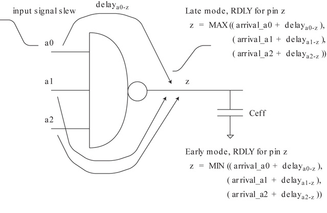
Figure 11.11 Illustration of late and early arrival time propagation in static timing analysis.
There is a methodology question associated with this forward propagation algorithm. The results of the cell delay arc calculations are used to select the (min, max) arrival time at the output. However, each of the candidate delay arcs has an associated output slew. The propagation algorithm needs to select a slew to launch to the RC interconnect load. A conservative approach would be to use the slowest slew (in late mode) among any of the candidate delay arcs; the combination of the latest output pin arrival and slowest slew avoids the accuracy uncertainty of propagating a late output arrival with faster output slew versus an earlier arrival with slower slew. If the timing endpoint tests pass with this conservative calculation, no further investigation would be needed. If timing tests fail and debugging is needed after running the timing analysis flow, it is necessary to use the EDA vendor tool to select detailed paths through user-defined sets of cell pins and recalculate the specific arcs and slews.
The general delay propagation method utilizes a levelized cell network between timing testpoints (e.g., flop-to-flop, PI-to-flop, flop-to-PO). A clk_ enable-to-clk timing test is included for gated clock cells. This method does not utilize any simulation testcase vectors to sensitize specific cell input-to-output (functional) transitions; as a result, this flow is denoted as static timing analysis (STA). A key advantage of this approach is the comprehensive analysis of all potential signal paths. As there is no logical evaluation of the network, a method is needed to prune timing paths that are not able to be exercised, as discussed shortly.
Although there is no logical evaluation of the levelized network, there is a logical property of the cell that is pertinent to STA. The library data for each cell input pin includes a unateness property that identifies whether the cell output will invert the input pin transition (e.g., NOT, NAND, NOR, AOI) or is positive unate (e.g., BUFFER, AND, OR) or is binate (e.g., XOR). This designation is needed to evaluate and propagate RDLY and FDLY arcs correctly.
11.4.1 Timing Slack Calculation
A signal arrival time that fails a test at a timing path endpoint is indicative of the need to make an engineering change to the physical design. However, in a large network with potentially many failing tests, the SoC designer would need additional insight into where to focus timing optimizations. The concept of timing slack is used to identify the criticality of all input and output cell pins in the timing model, as depicted in Figure 11.12.
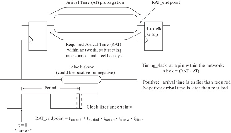
Figure 11.12 Illustration of the timing slack calculation in the static timing analysis flow.
The forward propagation of calculated cell and interconnect delays provides the arrival time (AT) at each pin. The timing test involves a comparison between the AT and the required arrival time (RAT) at the path endpoint. In late mode, the endpoint RAT is derived from the setup time constraint, the clock period specification, the clock launch-to-capture skew, and clock jitter margin. If the network timing model were to be traversed in reverse levelized order from the endpoint RAT, subtracting the cell and interconnect delays, a specific RAT value could be assigned to each pin internal to the network.
For a cell output pin, the late mode RAT is the “earliest” required time traversing back from the fan-out pins through interconnect delays. The (RAT – AT) difference at each pin is denoted as the (late mode) timing slack. A positive slack indicates a forward propagation arrival time that precedes its required arrival time, as derived from the backward calculation from all timing path endpoints. A negative slack indicates an arrival time that is later than its required arrival and, thus, needs to be addressed.
In early mode, the AT propagation uses minimum path delay calculations, as depicted in Figure 11.11. The RAT at the timing endpoint is based solely on the clock skew, clock jitter, and hold time constraint of the flop cell. For early mode timing analysis, the timing slack is the (AT – RAT) difference. If the AT is earlier than the RAT, the timing slack is negative, and a hold time error is reported. A similar backward calculation through the network using the “latest” required time through fan-out interconnect delays determines the RAT and the early mode slack at all cell output pins.
The advantage of the timing slack formulation is that it quickly identifies the cells internal to the network that have a large sensitivity to timing closure (see Figure 11.13).

Figure 11.13 Negative slack nodes in the timing network identify cells with high sensitivity to path timing closure.
Cells with a large negative slack are the primary candidates for (late mode) timing optimizations:
Update the cell drive strength.
Update the cell Vt selection.
Restructure the cell netlist to implement different fan-out repowering.
Modify the wire layer/width/spacing for segments in the fan-out interconnect tree.
If the fan-out tree from a negative slack cell has a wide range of slacks, offloading non-critical fan-out may significantly improve the overall timing closure, as illustrated in Figure 11.14.

Figure 11.14 Illustration of fan-out restructuring at a negative timing slack network node.
EDA vendor STA tools offer an interactive session feature, with access to the existing timing model and the results from the STA flow. In addition to allowing the querying of the timing results data, the interactive environment allows the designer to inject timing model changes, such as the candidate cell swaps listed above. An incremental timing feature can assess the impact of the model edits on the timing results; for fastest response, the scope of the timing recalculation is limited rather than striving for highest accuracy with a full model recalibration. The output of interactive timing debug would be to generate a set of netlist ECOs that could be applied to the physical implementation. Cell and/or fan-out repowering changes would be placed, cell overlaps resolved, and affected routes updated.
11.4.2 Pin Constraints for STA
The timing paths for tests involving model PIs and POs utilize constraint data similar to that provided for the synthesis flow (see Section 7.2). The distinction for STA is that the actual clock arrival data are used as the timing test reference rather than the idealized clock latency and skew targets used during synthesis.
11.4.3 STA “Don’t Care” and “Adjust” Specifications
STA does not evaluate the logic functionality of the timing model (except the unateness) as part of the comprehensive approach to forward propagation of all potential network paths. As a result, there may be paths that are logically invalid. To exclude these paths, a directive to the STA flow indicates a timing don’t care (also known as a false path). The STA false path constraint would indicate the connections in the levelized timing graph for which propagation is not performed (e.g., a specific path with “from-through-to” pins or a larger sub-graph with “from-to” pins). Reference 11.9 describes an algorithm for efficiently removing edges in the timing graph, given a false path specification. Note that it is necessary to update the timing graph for false paths after delay calculation; the loading of the false path pins is included in the cell and interconnect delays, but the (max, min) arrival propagation step omits the false path cells. The SoC methodology should ensure that any false paths submitted to timing analysis are independently verified to avoid exclusion of a timing path that is indeed exercisable. Formal property verification would be appropriate to prove the validity of the false path constraint.
Another input constraint to the STA flow would be the identification of any multi-cycle paths (i.e., paths between testpoints that are by design expected to exceed the cycle time period specification), as illustrated in Figure 11.15.
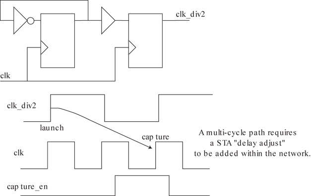
Figure 11.15 A multi-cycle logic path requires the addition of a delay adjust constraint in the static timing analysis flow.
In the figure, correct functionality is maintained when the capture flop is updated every other clock cycle. To present this case to the propagation phase of the STA flow, a delay adjust constraint is given; essentially, an artificial cell is added to the timing graph in the combinational data network with a “negative propagation delay” value. To test a two-cycle path, a delay adjust equal to one clock period would be added. The location in the timing graph for the delay adjust needs to be selected judiciously, as sub-graphs in the timing model may be part of both single- and two-cycle paths. Similar to the false path constraint, any multi-cycle delay adjusts provided to the STA flow should also be independently verified.
11.4.4 Timing Analysis Modes
In general, STA is performed without evaluation of the logic functionality of the netlist model. However, in some cases, an operating condition for the timing model defines a specific set of timing tests to be performed. Section 7.2 first introduced the concept of multi-mode analysis, in the context of timing-driven synthesis. Similarly, the STA flow can support functional modes. Logical values are assigned to specific signals in a separate mode file, along with related clock period and PI/PO constraints. These assigned values are functionally simulated to establish specific timing model paths for propagation.
The most general cell timing models may include state-dependent delays, where an input-to-output pin arc has multiple representations, based on specific logic values assigned to other pins during characterization. If this modeling approach is used, a timing mode requires recalculating delays before propagation and slack calculation.
A common use of a timing mode is to evaluate the paths associated with scan-shifting during test operation, as shown in Figure 11.16. The shift clock frequency from the tester is typically much slower than the system clock, and with the relatively short scan logic paths, setup time checking should be straightforward. The emphasis in the test timing mode would be on hold time checking, using the skew and jitter for the test clock distribution to calculate the RAT at each flop endpoint.

Figure 11.16 A timing mode is included for scan shift paths.
Another common application of timing modes relates to unique timing tests associated with an embedded IP macro. The macro timing model from the IP vendor could include multiple sets of timing constraints, whose values depend upon the specific operation being performed. For example, an embedded SRAM array may have different address/data setup constraints to the array enable input for a read operation compared to a write access. The SoC timing team needs to develop the static timing analysis modes and timing model inputs to enable verification of the different operations.
11.4.5 Reporting
The output reports from the STA flow offer (extremely) detailed delay and slack data for all pins, for all corners and modes. The first debug step is to sanity check the results. For example, a negative slack (of significant magnitude) may be indicative of a multi-cycle adjust that may have been inadvertently omitted or an additional timing mode that needs to be defined. The next step would be to explore potential updates to the timing model, using the EDA vendor’s interactive model viewer with incremental timing recalculation. From the updates to the model, an ECO netlist would be exported for physical implementation.
The design team may request a review of critical timing paths with the SoC methodology and CAD teams. There is potentially sufficient conservatism in the STA propagation method to warrant additional analysis of a failing path. A common feature of EDA vendor STA tools is to export a detailed netlist of a specified critical path—excising the cells, RC interconnect tress, side loads, and clock distribution. Note that the excised circuit simulation netlist requires attention to the k-factor applied to the coupling capacitances, which have been grounded for STA delay calculation. This netlist would be submitted for circuit simulation (at the corners of interest) to provide a more precise arrival time.
The results of the timing analysis flow are summarized in the project management scoreboard. A number of different results representations are commonly used—for example, the worst negative slack (WNS), the total negative slack summed for all failing paths (TNS), and a graphical distribution of all slack values (positive and negative) at timing test endpoints. The slack distribution is the most informative. For example, if a large number of failing paths are present, with small negative slack, the resources required to explore individual cell updates will be substantial. A review of other potential, more pervasive approaches would be warranted, such as a supply voltage increment, changes to the clock distribution to reduce the arrival skew, or modification of the design assumptions to adopt a useful skew implementation. As the tapeout schedule is likely fast approaching, the SoC and methodology teams need to be prepared to quickly address the possibility of a negative slack “timing wall” in the timing analysis path distribution curve. Finally, the review of the timing reports may result in waivers (due to assumed conservatism in timing margins), allowing the STA flow to be logged as “complete” in the SoC project management scoreboard.
11.4.6 Variation-Based Timing
The sources of manufacturing variation are more diverse in advanced process nodes, from interconnect RC tolerances due to CMP, to FinFET device fabrication parameter distributions, to layout-dependent effects. Parameter variations are derived from testsite data, measured across wafer lots, within each wafer, and within each die. As a result, the variations are typically associated with “global” and “local” distributions, as shown in Figure 11.17. The global and local n-sigma variation models used for library timing characterization are derived from measurements on device currents and extended to cell delay arcs. The figure depicts the statistical distribution of a cell delay arc at a specific voltage and temperature due to fabrication variations.
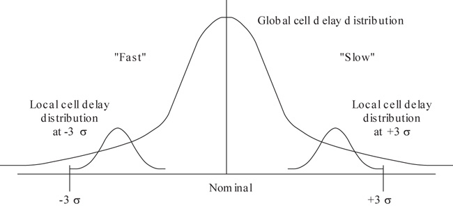
Figure 11.17 Global and local device cell delay distributions due to fabrication variation.
Characterization is initially performed using a set of process parameters to reflect an n-sigma slow and an n-sigma fast delay from the global distribution (typically n = 3). For variation-based timing analysis, the local distributions are also incorporated. The global delay curve in the figure represents the full variation across the manufacturing process. (As an aside, the global curve drawn in the figure is Gaussian. At leading process nodes, the delay distribution is decidedly non-Gaussian; implications of timing variation with non-Gaussian distributions are discussed in Reference 11.10. Also, most characterization flows generate the nominal delay arc tables, using the typical process parameters, at the voltage and temperature associated with the corner.)
Superimposed on the global delay curve are local distributions, in which the n-sigma endpoints of the two curves are aligned. Local parameter distributions would be applicable to within-die circuits, where there would be a degree of process tracking of parameter values in close proximity. The figure illustrates the proposal that a global worst-case (or best-case) delay characterization approach applied to all cells in the timing model would be conservative. A derating of these global delays to represent the probabilistic nature of local delays is appropriate. An analogy for the pessimism in the use of global delay models for path timing for all cells would be to schedule a cross-country driving trip. The conservative calculation of being in “rush hour traffic” through each major city is very unlikely; the more cities on the route, the more unlikely this would be.
To enable SoC designers to compensate for timing pessimism associated with this global and local delay distribution model, the EDA vendor STA tool likely includes a feature to apply a derating multiplier. A derating factor could be applied (selectively) to any of the delays in the timing model:
All delays
Cell delays (to all logic cells or by library logic cell name or by logic cell delay arc)
Interconnect delays
Specific cell instances (differentiating clock cell derates from logic cell derates)
Specific interconnect nets
By levelized position in a timing path
By relative location to other cells
Derating multipliers less than one (worst case, late mode) applied to logic cells in the timing model would be used to reduce expected pessimism in the global characterization, delay calculation, and propagation algorithms. Conversely, a multiplier greater than one would add conservatism to late mode logic paths. For early mode, a logic data path derating factor greater than one would reduce pessimism for hold time checks (although given the critical nature of satisfying hold time for functional operation, application of derates for a pessimistic hold assumption should be done judiciously).
A timing path example illustrating the use of cell derating factors is shown in Figure 11.18. The logic cells in the timing path would be given derate multipliers to reflect sampling from the local delay distribution. The cells in the clock path maybe given distinct derate values from the logic path. Also, note that levelized cells in the logic timing path would typically be assigned different derates, based on path position. For longer paths, the probabilistic sampling of variations will tend to result in an “average” cell delay closer to the local mean, for the sum of the cell delays in the path. Thus, the derate multiplier for a high-levelization-number cell is selected to provide a local delay for the cell further from the global characterization value to adjust the overall path delay accordingly.
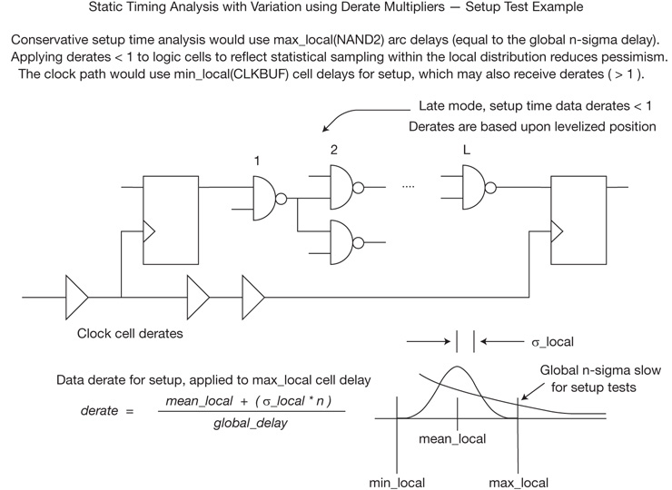
Figure 11.18 Illustration of cell delay derating factors. A setup timing test example is depicted.
To implement a derating strategy to address pessimism in timing model delay calculation with global and local variation—or, for that matter, to address potential optimism—the SoC methodology team needs to review the statistical characterization approach used by the IP provider. The foundry releases PDK models with statistical distributions based on fabrication testsites. These distributions reflect the overall global device and interconnect parameter data, measured from lot to lot, from wafer to wafer, and across the wafer. Additional distributions represent the local variation data within die, where the σlocal would be a function of the proximity of devices and interconnects on the testsite. The IP provider utilizes these statistical process distributions to establish the derate multipliers to help SoC designers address (late mode) pessimism in the STA flow. The IP provider releases derate tables, which are similar to NLDM tables, as illustrated in Figure 11.19.
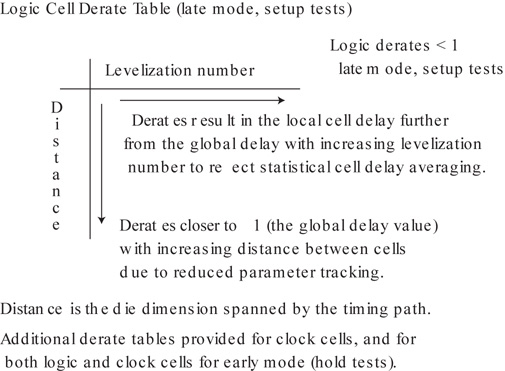
Figure 11.19 Example of a cell derate table to address late mode timing path pessimism. Rather than all cells using the global n-sigma arc delay, a set of local derate multipliers are applied to the characterization table value.
In the figure, the input parameters for cell delay derate multipliers are the physical distance spanned by the timing path and the “levelization number” of the cell. For larger dimensions spanned by the path, the “tracking” of local cell delays is reduced; the derate multipliers are closer to 1, which is the global delay value. For higher levelization numbers, the cell derate multiplier results in a delay further from the global n-sigma maximum to better reflect the statistical averaging of multiple local cells in the path.
The potential number of derate tables (and additional characterization effort) is large; recall that NLDM delay and output slew tables are provided for each cell arc across a range of input slews and output loads. Derate table generation for the delay and output slew for each cell would require significant (statistical, Monte Carlo sampling) simulation resources to derive the local distributions. For efficiency, the IP provider is likely to consolidate the derate tables considerably (e.g., one derate table per cell, selected across all arcs, slews, and loads). The path length and location dependency factors in the derate calculation are also determined using Monte Carlo–sampled simulations of representative cells and interconnect layouts, applying the local distributions from the foundry for both device and interconnect variations.
Derate factor tables may also be released by the IP provider for scaling delays with respect to supply voltage and temperature environment settings that differ (slightly) from the PVT characterization corner settings.
A newer proposed variation timing approach uses a different formulation. The cell characterization data would provide an NLDM-like table with σlocal values provided for delay arcs across input slew and output load ranges for each corner. A different statistical-propagation algorithm is now required within the STA tool, as opposed to the conventional max/min arrival time calculation, with scaled delays using derate multipliers. The timing test at the path endpoint also now becomes probabilistic, comparing clock and data distributions to establish a statistical confidence measure.[11]
It should be highlighted that the static timing methodology to represent increased process variation is still evolving. Timing analysis involves a complex interaction between PDK models, library cell characterization, and cell plus interconnect delay calculation. There are accuracy versus resource trade-offs throughout:
Circuit and interconnect extraction for various corners
IP characterization, including the definition of the setup/hold timing tests
Coupling capacitance modeling (e.g., the k-factors used in interconnect delay calculation)
Ceff calculation
Cell delay calculation (nominally measured as the 50 percent-to-50 percent input-to-output waveform crossing delay, with interpolation between the NLDM table entries)
Cell output waveform definition and interconnect delay calculation
Interconnect delay/slew calculation at cell fan-out pins
Local supply/ground (dynamic) voltage drop
Local temperature differences (on device and interconnect behavior)
With all these variables, the foundry, IP library provider, and EDA tool vendor are striving to define modeling and timing analysis methods that also adequately reflect process variation, without excessive pessimism (or, worse, optimism). The SoC methodology team must assess which variation-aware timing approaches are appropriate for their resource budget and schedule, relative to the design performance targets.
11.4.7 Delay-Based Timing Verification
The application of STA to VLSI methodologies has significantly diminished the use of simulation testcase-based delay testing. The comprehensive nature of STA evaluating all paths in the levelized network graph has effectively covered the need for functional simulation of the cell netlist with instance-specific delays. There are two applications where delay-based simulation may offer additional insights to the SoC design team:
The members of the test engineering team may wish to simulate specific test patterns to ensure that the chip pin input stimulus time and output pin strobe capture settings relative to the tester clock are valid.
The functional switching activity with instance-specific delays provides more accurate data on cell-level power dissipation.
Power estimation at the RTL level uses cycle-based simulation event traces on RTL signals and registers to gauge the switching activity. These estimates are extremely useful for relative power optimization decisions prior to physical design. The use of representative simulation testcases with a cell netlist-level model (with only delta delays) offers additional insight. Even if the cell instance delays are zero, more accurate functional switching activity factors are provided compared to the RTL estimates. However, if a delay-based netlist model is used, the results also provide insights into the glitch power due to combinational logic toggles within a cycle, as depicted in Figure 11.20.

Figure 11.20 Example of cell power dissipation due to a glitch transition within a clock cycle. This transition is not accounted for by static timing analysis, nor is it detected by (levelized) netlist simulation with zero-delay arcs.
zThere are several intricacies to enabling delay-based simulation, for both delay annotation and timing tests. The IP library HDL models need to incorporate the appropriate timing tests at the PVT corner corresponding to the power dissipation calculation. For complex macros and cores from IP providers, the internal event evaluation detail and checking in the functional model is likely to be quite limited. The SoC methodology team needs to review what delay-based model support is available for the IP and whether that meets the simulation testbench requirements. The STA tool needs to export the cell and interconnect delays in a format that can be annotated to the netlist instances. The EDA industry has established a de facto standard for netlist delay annotation; the Standard Delay Format (SDF) defines how timing model data is to be written by the STA tool and the interpretation of this file by an HDL simulator that supports annotation.[12] This cell delay format includes the capability to define a range of (min, typ, max) transition delay values, assigned to cell pins; the simulations need to select the delay value (or range of values) appropriate for the switching activity of interest.
Transport and Inertial Delay
The SoC methodology team needs to review the HDL simulator settings to be applied when events on the simulator queue are subject to preemption. Specifically, a new event may be associated with inertial or transport signal delay, as illustrated in Figure 11.21.

Figure 11.21 The distinction between transport and inertial delay for an HDL simulator is depicted for delay-based simulation.
An inertial delay property implies that a pending signal update on the simulator event queue would be preempted by a subsequent event of different value; the addition of the subsequent assignment to the queue includes removal of the pending event. The “inertial” response time of the signal would preclude the interim transition. A transport delay property is equivalent to a signal with infinite bandwidth; the new signal value assignment is added to the queue after the pending event, and both transitions are evaluated. A transport delay representation offers insight into the glitch switching activity. (There is also the unlikely situation in which a subsequent signal update would occur in time before pending events on the queue; in this case, all future events scheduled for times later than the most recently posted update would be preempted, regardless of the inertial or transport signal property.)
Delay-based simulation for timing verification has effectively been displaced by STA and is focused on specific power and test applications. The adoption of STA modeling based on cell arc and interconnect delays still allows timing model annotation to an HDL-based netlist, using an external delay file format. Delay-based simulation is complicated by the diverse sources of IP models and the focus by IP providers on representing timing tests in the timing model abstract, rather than the functional HDL.
11.5 Summary
Of the three primary PPA goals associated with an SoC design project, performance is commonly the most critical. Market expectations for a new product are usually based on the relative performance compared to existing offerings. SoC architects and physical implementation engineers focus on design optimizations to achieve timing goals—yet, the final sign-off decision is based on static timing analysis flow results.
Ideally, the measured silicon performance closely correlates to the critical paths identified by the STA flow. During silicon prototype evaluation, experiments are pursued to ascertain which paths fail as the clock frequency is increased beyond the product specifications. Hopefully, the STA slack distribution provides an accurate prediction of the silicon data for the passing clock period and the failing paths when the clock period is reduced. However, the accuracy of the static timing model remains a major focus area.
The methodology for STA strives to identify steps where delay calculation and/or path arrival propagation is conservative. The impact of a conservative timing model is twofold. Engineering resources are expended to “fix” negative slack paths that are indeed adequate, and the power/area targets could likely have been further optimized for a timing model with more accurate measures. As a result, there is significant methodology development to improve STA accuracy in collaboration with the foundry, IP library providers, and EDA vendors. Cell characterization models are incorporating more accurate output waveform detail for interconnect delay calculation. Derating strategies are being more widely adopted to better reflect an n-sigma timing result encompassing a complete levelized path, rather than for each individual cell in the path. Alternatives to the propagation of the latest output arrival and slowest output slew rate from all input pin arrival data are being used to further reduce the conservatism (refer to the “path-based” propagation method highlighted in the upcoming “Future Research” section).
As briefly mentioned in this chapter, considerable STA methodology development activity is ongoing to effectively represent PVT variations as a statistical distribution of individual cell and interconnect delays for the SoC design, and efficiently calculate the statistical arrival time through the levelized network. The result of statistical STA is a confidence level in achieving the overall performance target, rather than a slack value at each timing endpoint.
The methodology for STA with the optimum trade-offs between delay model plus propagation accuracy, flow throughput, and correlation to silicon data continues to evolve.
References
[1] Macys, R., and McCormick, S., “A New Algorithm for Computing the Effective Capacitance in Deep Sub-micron Circuits,” Proceedings of the IEEE Custom Integrated Circuits Conference (CICC), 1998, pp. 313–316.
[2] Qian., J., Pullela, S., and Pileggi, L.T., “Modeling the Effective Capacitance for the RC Interconnect of CMOS Gates,” IEEE Transactions on Computer-Aided Design of Integrated Circuits and Systems, Volume 13, Issue 12, December 1994, pp. 1526–1535.
[3] Elmore, W.C., “The Transient Analysis of Damped Linear Networks with Particular Regard to Wideband Amplifiers,” Journal of Applied Physics, Volume 19, Issue 1, 1948.
[4] Rubinstein, J., Penfield Jr., P., and Horowitz M.A., “Signal Delay in RC Tree Networks,” IEEE Transactions on Computer-Aided Design, Volume CAD-2, Issue 3, July 1983, pp. 201–211.
[5] Gupta, R., Tutuianu, B., and Pileggi, L.T., “The Elmore Delay as a Bound for RC Trees with Generalized Input Signals,” IEEE Transactions on Computer-Aided Design of Integrated Circuits and Systems, Volume 16, Issue 1, 1997, pp. 95–104.
[6] Alpert, C.J., et al., “Delay and Slew Metrics Using the Lognormal Distribution,” Proceedings of the 40th IEEE Design Automation Conference (DAC), 2003, pp. 382–385.
[7] Kar, R., et al., “Delay Estimation for On-Chip VLSI Interconnect Using Weibull Distribution Function,”2008 IEEE Region 10 and the 3rd International IEEE Conference on Industrial and Information Systems, 2008, pp. 1–3.
[8] Alpert, C.J., et al., “Closed-Form Delay and Slew Metrics Made Easy,” IEEE Transactions on Computer-Aided Design of Integrated Circuits and Systems, Volume 23, Issue 12, December 2004, pp. 1661–1669.
[9] Blaauw, D., Panda, R., and Das, A., “Removing User-Specified False Paths from Timing Graphs,” Proceedings of the 37th IEEE Design Automation Conference (DAC), 2000, pp. 270–273.
[10] Keller, I., and Ghanta, P., “Importance of Modeling Non-Gaussianities in STA in sub-16nm Nodes,” TAU Workshop, 2016. (Presentation slides available at http://www.tauworkshop.com/2016/slides/10_TAU2016_Ghanta_nonGaussian_POCV.pdf.)
[11] A brief description of the Liberty Variance Format (LVF) is provided by Bautz, B., and Lakanadham, S., “A Slew/Load-Dependent Approach to Single-variable Statistical Delay Modeling,” TAU Workshop, 2014. (Presentation slides available at http://www.tauworkshop.com/2014/Slides/Bautz_SOCV_TAU_2014.pdf.)
[12] IEEE 61523-3-2004: “IEEE Delay and Power Calculation Standards—Part 3: Standard Delay Format (SDF) for the Electronic Design Process,” https://ieeexplore.ieee.org/document/7386825/.
Further Research
Graph-Based Versus Path-Based Delay Analysis
The discussion in this chapter highlights a conservative methodology for static timing propagation at each cell; specifically, the latest input-to-output arc arrival time and the slowest output signal slew among all arcs are selected for (late mode) propagation. This approach is referred to as “graph-based” STA.
Describe the alternative “path-based” algorithm, with either NLDM or waveform tables.
Describe the runtime versus accuracy trade-offs between graph-based and path-based analysis—specifically, when and where path-based analysis is appropriate.
False Path Verification
Describe a methodology flow for independent verification of STA false path constraints.
STA Results to Be Recorded in the SoC Project Scoreboard
Describe the key information from the STA flow report to record in the SoC project methodology manager. Data to consider include the following:
Flow input timing constraints, corners, and modes
Assigned clock arrivals and skews (e.g., from a separate clock simulation flow)
Derate assumptions used for local n-sigma delay scaling
TNS and WNS, for both early mode and late mode
Slack distributions
Slacks for PI-to-endpoint and endpoint-to-PO paths (for budgeting review; see below)
Specific from-through-to failing paths (especially paths through hard IP macros, which may necessitate significant physical design updates)
Paths that have been excised and submitted to circuit simulation
Waivers (granted after a review of a path-based timing analysis for a from-through-to path or from detailed circuit simulation results)
Block-Level Timing Constraint Budgeting
Budgeting Methodology
A key methodology policy is how (and how often) to provide block-level pin timing arrival constraints, a step typically referred to as “budgeting” of the overall clock cycle time. A path spanning two blocks requires assigning driving output pin required arrival time and receiving input pin expected arrival time constraints, with an allocation of the global path delay interval. A multiple fan-out global net adds to the timing budget model detail, as global path delays may differ significantly to individual fan-out pins. In addition, timing constraint values are required for each timing corner and mode in support of MCMM static timing analysis. As individual block design teams exercise STA, local optimizations are evaluated to attempt to satisfy PI-to-endpoint and endpoint-to-PO failing paths. However, it may become evident that iterations on the budgeted timing constraints are required.
Describe a budgeting methodology for development and iteration on STA pin constraint values. Also assess when activity on block-level timing optimization with existing timing constraints should be concluded and when a project-wide iteration on timing budgets is appropriate. In addition, assess when a change to the global interconnect buffering design would be a preferred alternative.
Registered Input and Output Pins
To simplify timing constraint budgeting, vendor IP designs may include “registered” inputs and outputs, without significant logic path depth between the IP pins and timing path endpoints—perhaps just a flip-flop and buffer on an output pin and flip-flops on input pins. SoC block designers may also seek to architecturally add registers at block pins.
Describe the advantages and disadvantages of adding registered block pins relative to:
The timing budgeting methodology
Local block timing optimizations
The impact on global interconnect design
Overall SoC PPA targets
Global Repeater Insertion
A critical SoC design decision is whether to add a global repeater flip-flop to a signal between blocks. Modifications to global signal buffering topologies are an easier implementation decision than insertion of flop repeaters (assuming that the channel area is available). The decision to insert a repeater is especially disruptive if an issue arises later in the SoC project schedule. Ideally, paths requiring repeaters would be identified during initial global floorplanning; the area allocation, power and clock delivery, and SoC performance model would all reflect this decision. However, issues that arise during the physical implementation phase may require a design review.
Describe the budgeting methodology and STA results criteria that would necessitate a design review of global paths that were not previously identified as requiring a sequential repeater. Describe the various SoC design teams that need to participate in this review. If the decision is indeed made to add repeaters, describe the impact on SoC architectural, logical, and physical implementation models; also describe the impact on the functional validation testbenches.
Delay-Based Functional Simulation (Advanced)
Describe the features of an SDF file used to represent the cell and interconnect delay calculation data of the STA flow (for a specific MCMM setting).
Describe the required features of the HDL model for each library cell to support annotation of the SDF information for delay-based simulation. Illustrate these HDL features using either Verilog or VHDL cell model examples.
Describe how specific timing tests at flip-flops and hard IP macros would be represented in the HDL models in support of delay-based simulation.