
Chapter 12
Interfacing
An image processing system never stands alone. This is particularly the case for an embedded vision system, which is usually designed for one specific purpose or task. Therefore, there are usually one or more peripheral devices connected to the FPGA implementing the system.
Each device connected to the FPGA must have an appropriate interface within the FPGA. This is responsible for passing any data to or from the rest of the logic, including any format conversions required between the peripheral and the processor implementing the algorithm within the FPGA. It is also responsible for providing any control signals required by the peripheral device. This may range from a clock signal and simple handshaking through to complex protocol management. Many peripheral devices require initialisation or configuration through the setting of control registers.
The interface logic may be thought of as a device driver, shielding the image processing hardware from much of the lower level complexities of the physical interface (Bailey et al., 2006). The primary focus of this chapter is on some of the techniques associated with the design of such interfaces. The term device driver may be a little misleading in this context, as it is referring primarily to interface hardware. If the system is made of a mix of programmable hardware and software, then the interface between them will also be in the form of a software device driver (Williams, 2009).
It is also useful within this context to consider the interaction between the FPGA system and the user. On a hosted system, the host computer will perform many of these tasks, using the host operating system. On a stand-alone system, however, all of these functions must be performed on the FPGA. One advantage of including an embedded processor is to provide a high level software environment for managing user interaction. Such tasks tend to be control-centric, making them more difficult to implement directly within the FPGA fabric. Most user interaction is not time critical, so hardware acceleration is usually not necessary. However, in some applications, particularly in the context of real-time debugging, it may be desirable to implement some of these functions directly in hardware (Bailey et al., 2006; Buhler, 2007). This is a secondary focus of this chapter.
Many embedded applications are designed for performing a single task. Once configured, it is usually not necessary to change the configuration (apart from upgrading the application). Where dynamic configuration is used, it is most likely to be between predefined variants of an algorithm that are designed for specific conditions. Through reconfigurability, the algorithm is adapted to the current conditions. However, another use of FPGAs is for computation acceleration. In such cases, reconfigurability is more important depending on the particular task or task mix that is currently being executed. In this case it is important for the host system to be able to allocate a task or mix of tasks to an FPGA. This usually requires operating system support (Wigley and Kearney, 2001; So, 2007). Such techniques are beyond the scope of this book.
Before getting into details, there is one further general consideration that warrants discussion. Many external devices have their own natural clock frequency. It makes sense to interface with the device at its natural frequency. This will usually require that the low level driver span clock domains. The part of the interface that interacts directly with the hardware will be in the hardware clock domain. However, the part that connects to the core of the system will be in the main system clock domain. Since the domains are relatively asynchronous, it is important to consider the reliable communication between the domains, as discussed in more detail in Section 5.1.3. Buffer design is also important to ensure data is not lost in the transfer between domains.
In an embedded vision system, it is usually necessary to connect to a camera or other video input. There is quite a wide range of different camera formats and communication protocols, and each has its own interfacing requirements. While it is impossible to describe them all in any detail, the broad characteristics of most of them are introduced in the next section. Subsequent sections discuss particular interface issues: combining data from interlaced frames in the presence of motion; correcting the distortion associated with rolling shutter; and recovering colour data from a raw image captured with a Bayer pattern.
12.1.1 Camera Interface Standards
12.1.1.1 Analogue Video
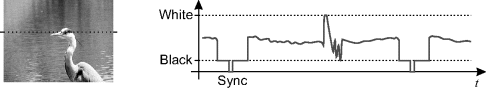
A monochrome analogue camera encodes the video signal as an analogue voltage level that is proportional to the light intensity at a point in a scene. The output follows an interlaced raster scan, with the horizontal position coded with time, as illustrated in Figure 12.1. Sync pulses at the end of every scan line and every field are used to synchronise the system.
Figure 12.1 Analogue video signal. Left: input scene; right: video signal for the marked line. (Photo courtesy of Robyn Bailey.)
There are three common techniques for representing colour information. Component video has three separate signals, one for each of the red, green and blue components. S-video (also called Y/C) has two signals, one for the luminance and one for the chrominance. The two components of the chrominance are typically encoded by modulating a colour subcarrier with quadrature modulation (the SECAM standard uses frequency modulation instead). Composite video combines the luminance and chrominance together as a single signal.
There is also a range of different video standards. For NTSC, the signal consists of 525 scan lines (480 with actual video data) with a frame rate of 60 Hz. However, in both PAL and SECAM the signal has 625 lines (576 active) at a frame rate of 50 Hz.
Figure 12.2 is a block diagram showing the steps in the conversion of a composite video signal to digital before processing on an FPGA. The conversion to digital is shown here as the last step, but this can be moved to anywhere within the processing chain. Technically, it is possible to directly convert the incoming composite video signal to digital and perform all of synchronisation and colour separation within the FPGA. However, this is not recommended because the processing is quite complex and would use considerable resources on the FPGA. The required processing is also different depending on the particular video standard that is input. Instead, using an analogue video decoder chip will perform all of these functions, and most will automatically detect the signal standard and perform the appropriate processing.
Figure 12.2 Typical functions performed by an analogue video codec.
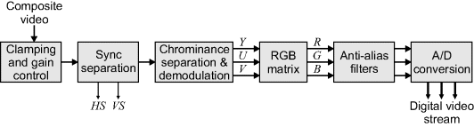
Communication with the codec usually has two forms. The digital video stream, along with the pixel clock, horizontal and vertical sync signals are available in parallel and can be connected directly to the FPGA. Codec configuration (setting the gain, saturation control, signal standard, output format) and status query is often through a separate interface. Since this is much lower speed, a serial communication protocol such as I2C is often used. Interfacing to I2C is described in more detail in Section 12.3.2.
12.1.1.2 Direct Interface
Analogue cameras are increasingly being displaced by digital video cameras. These allow a much wider range of resolutions and directly provide a digital signal. In an embedded device, the best approach is to interface directly to the digital sensor chip. Direct interface is usually much the same as connecting to an analogue codec. The digital pixels are streamed from the sensor, with line and frame valid signals. Sensor configuration (shutter speed, triggering, gain control, windowing, subsampling mode) is controlled through a set of registers. Again a lower speed serial communication protocol is often used for this.
In a CMOS sensor each of the pixels are potentially individually addressable. Although such in interface is not usually provided to the user, several operating modes exploit this ability. Some of these modes commonly made available to the user are:
- Windowing Rather than read out the entire image each frame, windowing allows a rectangular region of interest to be selected and only those pixels are read out. This allows the frame rate to be increased by reducing the area of the sensor that is read out. One application of this is object tracking in situations where the object being tracked only occupies a small fraction of the image area.
- Skipping An alternative to windowing is skipping, where the number of pixels read out is reduced by skipping entire rows or columns. This reduces the pixel count without affecting the field of view.
- Binning Rather than skipping pixels, adjacent pixels can be combined together. This has two advantages over skipping. Firstly, it reduces aliasing around sharp edges because adding adjacent bins is a form of low pass filtering. Secondly, since each pixel contributes to the output, binning can improve the sensitivity in low light conditions. Binning often has a lower frame rate because internally multiple pixels must be addressed to produce each output pixel.
A disadvantage of direct connection to the sensor is that the signal path between the sensor and FPGA must be kept short to maintain close control over timing and signal integrity. The alternative to direct connection is to use off-the-shelf cameras with standard interfaces.
12.1.1.3 Firewire and USB
Many consumer cameras have a USB or Firewire interface. These can be more difficult to interface directly to an FPGA. This is particularly so for USB, which relies on a host processor to manage the low level protocol. Firewire, on the other hand, is a peer-to-peer communication link and does not require a host processor for data transfer.
With both Firewire and USB, direct connection and signalling by the FPGA are impractical and will make inefficient use of resources. The best approach is to use an external chip that manages the physical signalling (a PHY chip). Such chips manage the high speed electrical signalling and convert the serial data into parallel data. The FPGA interfaces to the PHY chip at a speed that is easier to handle. However, this is still complex to interface because of the complexity of the protocols.
This is particularly so for USB, where the FPGA has to act as the host controller for the USB camera. It is also necessary to build considerable logic for managing the communication protocols. This ranges from sending packets to set up the image capture, to receiving and interpreting the video data packets from the camera. A further complexity is that some inexpensive webcams use proprietary protocols and compression – interfacing to these requires reverse engineering the USB protocols, not a trivial task! To connect a USB camera to an FPGA, the simplest approach is to have an embedded processor and interface to it through the appropriate software drivers. If it is necessary to connect directly from the FPGA logic to the USB, it is best to obtain an intellectual property (IP) block that manages all of the USB protocol details.
Interfacing with a Firewire camera is a little easier. Again it is necessary to use the PHY chip. The interface is made easier by a link layer controller (LLC) chip, which manages the communications protocol, CRC checking and provides a FIFO buffer for data. Some manufacturers provide integrated PHY and LLC, which provide a set of control registers through a microprocessor type of interface, and provide direct access to the streamed data through a DMA style of interface These can be connected directly to an FPGA, with a relatively simple controller to manage the application data built within the FPGA logic.
Firewire, as defined by the IEEE 1394 standard, divides all activity on the Firewire bus into 125 µs cycles. Each cycle is initiated by one of the nodes designated as the cycle master, which broadcasts a start packet allowing all other devices to synchronise with the bus. The remainder of the cycle is split amongst two types of data transfer. Isochronous transfers occur first; these are broadcast transfers designed for transferring large blocks of data. Up to 80% of the cycle time can be spent on isochronous transfers, shared amongst all the devices using the bus. The remaining time is for asynchronous transfers, which are point-to-point, with error recovery available.
Within this structure, there are two commonly used video standards or protocols that are used to control the device and transfer of video data. Industrial or machine vision cameras generally use the DCAM specification (1394 Trade Association, 2004), for the transfer of raw video data without audio. Many consumer devices use the AV/C (audio video control) protocol, also specified by the 1394 Trade Association. This defines the behaviour of digital audio-visual devices. The two protocols are quite independent and are not interoperable. The DCAM protocol is described here; the greater complexity of AV/C (because it must handle a wider range of devices) is beyond the scope of this section.
The DCAM protocol specifies a set of enquiry and command registers within the camera. The enquiry registers are queried and command registers set through asynchronous Firewire transfers. These allow the capabilities of the particular camera to be determined, and the camera to be initialised for the desired video mode, frame rate and other camera parameters (gain, white balance, shutter control, iris and focus control, and any other controls that may be offered by the camera). It is also necessary to set the isochronous channel number and bandwidth for transferring the video data and initiate the image capture process. The camera then streams the requested video data isochronously until instructed to stop. Since the asynchronous and isochronous transfers are independent, it is possible to communicate with the camera while it is streaming video data.
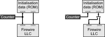
Overall, there are two initialisation phases in connecting to a Firewire camera. The first is to set up the Firewire LLC and the second is to set up the camera. With a microprocessor interface, unless an embedded processor is being used, it is necessary to build a small controller on the FPGA that provides the register address and corresponding data to set up the Firewire chipset. Figure 12.3 shows basic structure of a simple controller. The initialisation data is held in a ROM (implemented using fabric RAM). If the registers can be programmed sequentially, the counter steps through the ROM providing the data associated with each address. If the registers must be accessed multiple times, or in a random order, then the alternative is to store both the LLC address and data within the ROM and use the counter to access these sequentially.
Figure 12.3 A simple controller for setting the link layer controller registers through a microprocessor interface. Left: sequential register addresses; right: register addresses in random order.
A similar type of structure can be used to initialise the camera. The difference is that this data is sent via asynchronous Firewire transfers. The process is easiest if a specific camera with known properties is being used. Otherwise, it is necessary to send a set of queries to the camera to first determine whether or not the camera supports the desired modes. The more complex logic required to manage a range of different cameras and to send the appropriate setup commands is probably best handled through a serial processor rather than within the fabric of the FPGA.
One example of a description of a dual camera system interfaced with an FPGA is described by Akeila and Morris (2008). They connected two Firewire cameras to an FPGA as part of a stereo matching system.
12.1.1.4 Camera Link
While USB, and to a lesser extent Firewire, are targeted primarily at the consumer market, when connecting to a digital frame grabber within an industrial vision system, the Camera Link interface (AIA, 2004) is more common.
Camera Link is based on National Semiconductor's Channel Link technology. A single Channel Link connection provides one-way transmission of 28 data signals and an associated clock over five LVDS pairs. One pair is used for the clock, while the 28 data signals are multiplexed over the remaining four LVDS pairs. This requires a 7 : 1 serialisation of the data presented on the inputs.
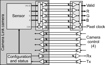
The base configuration for Camera Link camera is shown in Figure 12.4. It has (AIA, 2004) one Channel Link connection, with the 28 bits allocated as 24 bits for pixel data (three 8-bit pixels or two 12-bit pixels) and 4 bits containing frame, line and pixel data valid signals. The pixel clock has a maximum of rate of 85 MHz. In addition, there are four LVDS pairs from the frame grabber to the camera for general purpose camera control. The use of these is defined by the particular camera manufacturer. Finally, two LVDS pairs are provided for asynchronous serial communication between the camera and frame grabber. The serial communication is relatively low speed – the specifications say that a minimum rate of 9600 baud must be supported.
Figure 12.4 Base configuration for a Camera Link camera.
For higher bandwidth, the medium configuration adds an additional Channel Link connection for an additional 24 bits of pixel data. The full configuration adds a third Channel Link, giving a total of 64 bits of pixel data. This may allow, for example, up to eight pixels to be transmitted in parallel from the camera with each pixel clock cycle.
Modern FPGAs provide direct support for LVDS signalling. For the high speed pixel data, there are two choices. One is to use a Channel Link receiver chip to deserialise the high speed data and provide the pixel data to the FPGA in parallel. Alternatively, since there is no complex protocol involved, the multiplexed signals could be connected directly to the high speed inputs of the FPGA and the built-in SERDES blocks used to perform the 7:1 deserialisation and demultiplexing.
12.1.1.5 GigE Vision
Higher performance devices are tending towards using gigabit Ethernet for data communication. High speed or larger area image sensors are no exception. GigE Vision is a camera interface standard developed by the Automated Imaging Association that uses gigabit Ethernet for the transport of video data and sending control information to the camera. Because it builds on the back of the gigabit Ethernet standard, it is able to make use of low cost standard cables and connectors. These allow data transfer at rates of 100 Mpixels per second over distances up to 100 metres.
The GigE Vision standard has four elements to it. A control protocol defines the communication required to control or configure the camera. A stream protocol defines how the image data is transferred from the camera to the host system. Both of these protocols run over UDP. A device discovery mechanism provides a way of identifying which GigE Vision devices are connected and obtaining their Internet addresses. Finally, an XML description file provides an online data sheet that specifies the camera controls and image formats available from the device. The structure of this XML data sheet is defined by the GenICam standard (EMVA, 2009).
The design of a GigE Vision based system is an advanced topic and a detailed discussion of all of the issues is beyond the scope of this book. Only a brief overview is provided in the following paragraphs.
The complexities of the Ethernet protocol make a pure FPGA implementation difficult. To connect a GigE Vision camera to an FPGA would use a significant fraction of the FPGA resources just to receive the data. A reference design is available from Sensor to Image (2009c) for a GigE Vision receiver that streams data in from a camera and displays the resultant video on a VGA output. In most embedded vision applications, it would be more practical to build the FPGA system within the camera and perform any processing before sending the results to a host system using GigE Vision. Sensor to Image also provides reference designs for GigE Vision transmitters for both Xilinx and Altera FPGAs (Sensor to Image,;).
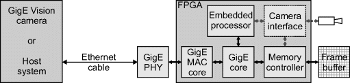
The basic structure of a GigE Vision system is shown in Figure 12.5. Unless the FPGA has a built-in gigabit Ethernet PHY this must be provided as an external chip. The MAC core may either be internal or external to the FPGA. The GigE core manages the low level networking features, routing the video stream to or from the frame buffer memory. The control protocol is routed to the embedded processor, which manages the camera configuration in software. When acting as a camera, the system also needs to interface with the sensor. This also provides an interface to the embedded processor for control of the actual camera and to the memory controller for saving the images to the frame buffer. In such a system, the embedded processor also makes available to the GigE Vision side the GenICam-based XML data sheet describing the capabilities of the camera. Not shown in Figure 12.5 is the image processing that adds value to the system!
Figure 12.5 Structure of a GigE Vision based system.
Real-time operation is achieved on the host system by using a dedicated device driver. This bypasses the standard TCP/IP protocol stack for the video stream, instead transferring the data directly to the application using DMA transfers. This eliminates any CPU overhead from the handling the actual video data as it is transferred.
12.1.2 Deinterlacing
Most analogue cameras use an interlaced scan. The frame is split into two fields, with the even rows scanned in the first field and the odd rows scanned in the second. For a stationary object or camera, this presents no problem, but if either the camera or objects within the scene are moving, then there is a displacement between the two fields.
There are two problems associated with interlacing. The first is the interlace artefacts associated with object motion relative to the camera. The second is associated with scan-rate conversion, for example when displaying video from a 25 frame per second PAL camera on a 60 Hz non-interlaced VGA display.
Consider first the conversion from an interlaced scan to progressive scan, with the output frame rate being double that of the input (so each field is converted to a full frame). Each input field only has half of the lines available. Let the ![]() th field be
th field be ![]() , where the missing lines are
, where the missing lines are ![]() for
for ![]() . The problem is then to estimate the data within the missing lines. This is an interpolation problem, with solutions involving both spatial and temporal interpolation.
. The problem is then to estimate the data within the missing lines. This is an interpolation problem, with solutions involving both spatial and temporal interpolation.
There is a wide range of methods that may be applied to this problem (de Haan and Bellers, 1998), with the more complex methods detecting the motion of objects within the scene and using motion compensated interpolation. One of the simplest methods that gives reasonable results on many images is a simple three-point median filter:
For static scenes, this is effectively just providing a median filter on the missing rows. This will have little effect on edges, but may cause a small reduction in fine detail. Where there is motion, the previous field may be incompatible with the current field as a result of the motion of edges. In this case, the pixel from the previous field will be quite different from the adjacent pixels in the current field. The median will therefore select either the pixel above or the pixel below to replace the incompatible pixel.
When performing frame rate conversion as well, then the best approach is to use full temporal interpolation. This detects the motion of objects and renders the object in an appropriate position according to the current frame time and object motion. If, however, a small amount of inter-frame judder can be tolerated, then the three-point median approach of Equation 12.1 can also be applied. To avoid tearing artefacts, it is necessary to work with complete fields. Equation 12.1 is simply applied to the two most recent complete fields at the start of the output frame. Incoming fields are simply buffered while the output is being produced. For example, to convert from 50 interlaced fields per second to 60 progressive frames per second, it is necessary to buffer four fields: the two that are currently being interlaced for the display and two to allow for an incoming field to be completed while the output frame is still being produced.
12.1.3 Global and Rolling Shutter Correction
The exposure time within a CMOS sensor is from the time that the pixel reset is released until the pixel value is read out. With global shuttering, all pixels are released simultaneously. The consequence is that pixels read out earlier will have a shorter exposure than those read out later. For short exposure times, there can be a significant difference in exposure between the first and last row read out, resulting in the top of the image being under-exposed and the bottom of the image being over-exposed.
This problem may be overcome in two ways. One is to use an external mechanical shutter to expose the image for a constant time. The alternative is to use an electronic rolling shutter. The reset for each row is successively released so that the time between release and readout is constant for each row. While this solves one problem, it introduces another.
If any objects within the scene are moving (or if the camera is moving or even panning) then since the different rows are exposed at different times, the output image will appear distorted. The nature of this distortion will depend on the relative motion between objects in the scene. For a stationary camera, any stationary background is unaffected. Any downwards motion will result in objects appearing stretched vertically, while upwards motion will result in vertical compression. Sideways motion will result in a shearing of the object. More complex motions, for example resulting from the panning of the camera, can result in additional rotation of objects within the image as a result of the change in perspective. Additional effects can be observed with light variations, for example when the scene is illuminated by fluorescent lights (Nicklin et al., 2007) where the periodic variation of light intensity appears as a distinct banding within the image.
Compensation for the rolling shutter requires modelling both the image capture process and the relative motion between objects and the camera (Geyer et al., 2005). A global correction is only applicable if the scene is stationary and the camera motion can be modelled (Nicklin et al., 2007; Liang et al., 2008). Otherwise, the motion of individual objects must be determined with the position of each object in each frame corrected accordingly. This is still an area of active research, with detailed algorithms not available at present apart for simple cases such as global motion.
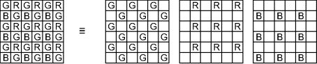
12.1.4 Bayer Pattern Processing
Most single-chip cameras obtain a colour image by filtering the light falling on each pixel using a colour filter array – essentially a mosaic of filters. The most common pattern is the Bayer pattern (Bayer, 1976), as shown in Figure 12.6. Each pixel receives light only of a single colour, with half of the pixels green, one quarter red and one quarter blue. Therefore, to form a full colour image, it is necessary to interpolate the missing values in each of the component images so that there is an RGB value for each pixel. This interpolation process is sometimes called demosaicing, because it is removing the mosaic of the colour filter array. The interpolation filters are spatially dependent because the particular filter function depends on the position within the mosaic.
Figure 12.6 Bayer pattern. Left: raw image captured; right: component colour images.
The simplest form of filtering is nearest neighbour interpolation. For the red and blue components, this is accomplished by duplicating the available component within each 2 × 2 block. Within the green component, the missing pixels may be obtained either from above or to the left. While nearest neighbour interpolation is simple, it does not really improve the resolution, with the image appearing blocky, particularly along edges. This requires a 2 × 2 window, with multiplexers to route the buffered pixels to the appropriate colour channels, as shown on the left in Figure 12.7.
Figure 12.7 Basic Bayer pattern processing. Left: nearest neighbour interpolation; right: linear interpolation. The letters within the multiplexers refer to the current output position, where G1 is the green pixel on the red row and G2 is the green pixel on the blue row.
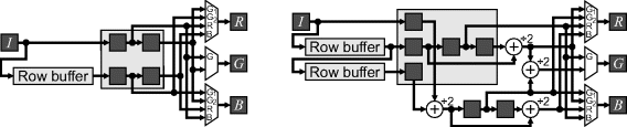
An improvement may be gained by using linear interpolation. The missing red and blue components with two horizontal or vertical neighbours are obtained by averaging the adjacent pixels vertically. Those in the middle of a block are obtained by averaging the four neighbouring values. This requires a 3 × 3 window, as shown in Figure 12.7. The vertical average may be reused to reduce the computation required. The divide by two from the averaging is free in hardware.
Using linear interpolation can result in blurring of edges and fine detail. Since a different filter is applied to each colour channel, this can result in colour fringes around sharp edges and fine lines. To reduce the blurring and consequent colour artefacts, it is necessary to detect the orientation of any features within the image, and perform any interpolation in the direction along the edges rather than perpendicular to them. This is complicated by the fact that only one colour component is available for each pixel.
To obtain an accurate estimate of the position of the edge, a much larger window and significantly more computation is required. There are many more complex algorithms described in the literature; a few examples are mentioned here. The ratio between the colour components at each pixel can be iteratively adjusted to make them consistent on each side of an edge (Kimmel, 1999). While this method handles edges reasonably well, the underlying assumption is that there are several consistent samples on each side of an edge. This is not the case with textured regions and fine detail results in colour fringing effects. This approach of enforcing consistency between colour channels is taken further by Gunturk et al., (2002), where the image is first decomposed into low and high frequency bands using a form of wavelet transform before applying consistency constraints within each band. An alternative to interpolation is extrapolation. The missing value is estimated by extrapolating in each of the four directions and using a classifier to select the best result (Randhawa and Li, 2005). A limitation of this approach is that it requires a very large window, making it less practical for FPGA implementation.
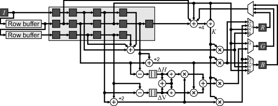
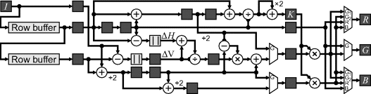
The final result will inevitably be a compromise between interpolation quality and the computation and memory resources required. One relatively simple algorithm that provides significantly better results than simple interpolation with only modest increases in computation is that by Hsia (2004). An edge directed weighting is used for the green channel, with simple interpolation used for the red and blue channels. However, the results are then enhanced using a local contrast-based gain to reduce blurring across edges.
Firstly, the edge directed weighting requires the horizontal and vertical edge strengths to be estimated:
(12.2) ![]()
(12.3) ![]()
Then, these are used to weight the horizontal and vertical averages:
If the denominator is zero, then the two weights are made equal at 0.5.
The interpolated output values are scaled by the local contrast based gain, which is calculated horizontally to reduce the number of row buffers required (Hsia, 2004). The gain term, ![]() , is:
, is:
where ![]() is the previously calculated output for the colour channel corresponding to the input pixels. The final value is the product of Equations 12.4 and 12.5. A similar gain term is used for the interpolated red and blue channels.
is the previously calculated output for the colour channel corresponding to the input pixels. The final value is the product of Equations 12.4 and 12.5. A similar gain term is used for the interpolated red and blue channels.
A direct implementation of this scheme is shown in Figure 12.8. The outputs are fed back through a multiplexer to select ![]() for the channel that determines the gain term. The effective window size is 5 × 3, requiring only two row buffers as with the simple bilinear interpolation.
for the channel that determines the gain term. The effective window size is 5 × 3, requiring only two row buffers as with the simple bilinear interpolation.
Figure 12.8 Direct implementation of the demosaicing scheme of Equations 12.4 and 12.5.
One limitation of this circuit from a real-time implementation is the feedback term used to calculate the local gain. The propagation delay through the division, multiplication and two multiplexers cannot be pipelined, and will therefore limit the maximum pixel clock rate. Potential alternatives for ![]() are:
are:
or
(12.7) ![]()
although this latter gain term will require an additional two row buffers. The multiplication by three or five may be performed by a single addition either before or after the division.
This circuit of Figure 12.8 may be simplified by reusing parts of the filter and factorising Equation 12.4 to give Figure 12.9. The local gain term uses Equation 12.6 to remove the feedback and the number of multiplications by ![]() was reduced from four to two by observing that only two of the results will be used for any particular output. An additional stage of pipelining has been added to perform the division and multiplications in separate clock cycles.
was reduced from four to two by observing that only two of the results will be used for any particular output. An additional stage of pipelining has been added to perform the division and multiplications in separate clock cycles.
Figure 12.9 Simplified logic for colour filter array demosaicing.
Just as image capture is important for an embedded image processing system, most imaging systems also need to be able to display images, even if just for debugging. There are two components to displaying an image, or indeed any other graphics, on an output from an FPGA. The first is the display driver that that controls the timing and generates the synchronisation signals for the display device. The second is generating the content, that is controlling what gets displayed where and when.
12.2.1 Display Driver
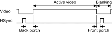
The basic timing for video signals was introduced in Figure 1.3. The image is sent to a display in a raster scanned format. At the end of each line of active video data there is a blanking period (Figure 12.10). During this blanking period, a synchronisation pulse is used to indicate to the monitor to begin the next line. For CRT monitors, the blanking period is typically 20% of the scan time for each row. This allows time for the scanning electron beam to be repositioned for the next line. A similar timing structure is used at the end of each frame to synchronise the monitor for displaying the next frame.
Figure 12.10 Horizontal video timing.
The Video Electronics Standards Association has defined a set of formulae which define the detailed timing for a given resolution and refresh rate known as the coordinated video timing (CVT) standard (VESA, 2003). (A number of legacy industry standard timings are also listed in (VESA, 2007).) Within the CVT standard, there are two sets of timings: one for traditional CRT type monitors and one for more modern flat panel displays that do not require the long blanking period. The latter timings significantly reduce the horizontal blanking period, increasing the available bandwidth for active video and significantly reducing the pixel clock frequency. The polarity of the horizontal and vertical sync pulses indicate whether the CRT timing, the reduced blanking interval timing or a legacy timing mode is used. The CVT standard also indicates to the monitor the target aspect ratio by the duration of the vertical sync pulse.
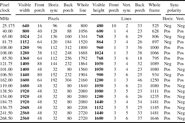
A number of common formats are listed in Table 12.1, along with the timing parameters for a refresh rate of 60 Hz. Parameters for other refresh rates may be obtained from standard tables or from a spreadsheet associated with the CVT standard.
Table 12.1 Timing data for several common screen resolutions for a refresh rate of 60 Hz (VESA,;)
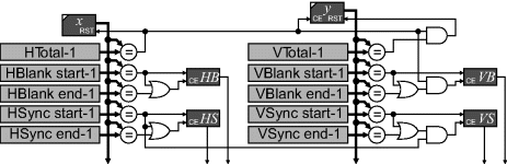
The timing can easily be produced by two counters, one for the horizontal timing along each row and one for the vertical timing, as shown in Figure 12.11. The count is simply compared with the times that the key events are required to generate the appropriate timing signals. Rather than use less than and greater than to compare when the counter is in a particular range, tests for equality reduce the logic. This requires an additional single bit register which is set at the start of the signal and cleared at the end. The vertical counter is enabled only when the horizontal counter is reset at the end of each line. The vertical sync pulse is also synchronised with the leading edge of the horizontal sync pulse (VESA, 2007). It is usual for the counters to begin at zero at the start of the addressable active region. In this case, the end of the blanking will correspond to the total, so one of the comparisons may be eliminated. However, if any stream processing pipelines require priming it may be convenient to advance the origin to simplify the programming logic.
Figure 12.11 Circuit for producing the timing signals for a video display.
12.2.1.1 VGA Output
The VGA output connector provides the display with analogue signal video signals for each of the red, green, and blue components. These require a high speed D/A converter for each channel. For simple displays, with only one or two bits per channel, these signals may be provided reasonably simply using a resistor divider chain. However, for image display the simplest approach is to use a video digital to analogue chip, which is available from several manufacturers.
In addition to the pixel data, separate horizontal and vertical sync signals also need to be sent. These need to be of appropriate polarity, according to the resolution and display mode used. CVT standard timings have positive sync pulses on the horizontal sync and negative pulses (normally high) on the vertical sync. Reduced blanking timings reverse these. Legacy modes may have both horizontal and vertical sync pulses high (or low). The sync pulses may be driven directly by the FPGA using 3.3 V TTL level signals.
The VGA connector also provides an I2C channel for communication between the host and the display. This is normally used for plug and play functionality, to enable the host to determine which resolutions and refresh rates are supported and for setting various display parameters. Generally it is not necessary to use this channel for driving the display from the FPGA provided that the particular resolution and refresh rate are supported.
12.2.1.2 DVI Output
One limitation of the VGA signal is that it is analogue, and therefore subject to noise. This becomes more acute at higher resolutions, which requires a higher pixel clock. The digital visual interface (DVI) standard (DDWG, 1999) overcomes this limitation by transmitting the signal digitally.
The red, green and blue pixel values are transmitted serialised using a transition minimised digital signalling (TDMS) scheme. This converts each eight bits of input data into a 10 bit sequence using a code that minimises the number of transitions and also averages out the DC level over the long term. The encoded signals are transmitted using a single ended differential pair. As a result of serialisation, the bit clock is 10 times higher than the pixel clock. Since there can be a wide range of clock frequencies (depending on the resolution and refresh rate), a pixel clock is also transmitted on a separate channel.
Four additional 10 bit code words are reserved for synchronisation. These are transmitted during the blanking period with the particular code word dependent on a pair of control signals. These control signals are normally zeros, however, on the blue channel, the control signal is made up of the horizontal and vertical sync signals.
The DVI connector comes in a number of configurations that differ in which signals are connected. The single-link digital connector contains the three data signals described above plus an I2C-based data channel for communication as described within Section 12.2.1.1. The maximum pixel clock frequency is 165 MHz. This is where the reduced blanking timings come in useful – they increase the useful bandwidth enabling a lower clock frequency to be used. Where the pixel clock exceeds the maximum, additional pins are used to provide a dual link, with two pixels transmitted in parallel each clock cycle. For backwards compatibility, the analogue video signals can also be provided, enabling a simple adaptor to be used with both digital and analogue monitors.
While the 8/10 bit encoding could potentially be performed on the FPGA (for example using a lookup table), a SERDES block would be required by each channel to meet the required data rates. DVI transmitter chips are also available which remove this logic from the FPGA with just a parallel data output for each channel.
12.2.1.3 Television Output
An analogue television signal combines the red, green and blue signals together, producing luminance and chrominance components, with the chrominance signals used to modulate a subcarrier. The processing for this is best performed using an external composite video signal codec.
For digital television connections, the HDMI standard interface using RGB mode is compatible with DVI and just requires a suitable adaptor.
12.2.2 Display Content
The second part of displaying any output is to produce the content that is required at the appropriate time. In particular, this requires producing each output pixel value at the correct time for the corresponding object or image to appear on the display.
The conventional approach used in software-based systems is to represent the content that is to be displayed as an array of data within memory (a frame buffer). This is then streamed to the display as required. The limitation of this approach is that the data to be displayed is calculated and written to a memory. Then, the contents of that memory is periodically read and streamed out to the display. To reduce flicker effects when updating the contents, a double buffering scheme is often used. A copy is made of the display image, which is then updated independently of what is being displayed, and then rapidly written back to the frame buffer to change the display smoothly. The cost of such an approach is that a significant fraction of the time may be spent reading from and writing to memory. Arbitration logic is also required to avoid access conflicts with the process that is reading from the frame buffer to actually display the image.
Using random access processing on an FPGA, like its software counterpart, requires a frame buffer to hold the image being displayed. Generally, double buffering, or bank switching, is also used to give a clean display and meet the bandwidth requirements of both image generation and display driver processes.
However, using stream processing on an FPGA provides an alternative approach. By synchronising the image processing with the display driver, it is possible to perform a much of the processing on the data as it is being displayed. To guarantee that the data is always available when it is needed it is necessary that the processing has a fixed latency. The processing is then started in advance of when it is required. This is made possible since the display driver produces regular, predictable signals, enabling the processing to be begun at precisely the right time. The fixed latency requirement may also be relaxed if necessary by introducing a FIFO buffer to take up any slack. In such cases the blanking periods at the end of each line and each frame may be used to catch up and refill the FIFO buffer.
Even within such a rigid processing regime, considerable flexibility is possible. For example, the display can be segmented, with different images or stages within the process displayed in each section.
12.2.2.1 Windows
This concept may be extended further to display each image within a separate window on the display. Dynamic windows allow the content to be resized and repositioned, giving greater flexibility over fixed image locations (Bailey et al., 2006). Each window requires a separate data structure containing the window properties, including a z-index which controls the order they appear on the display (Buhler, 2007).
The basic principle of on-the-fly display may be extended to the display of window contents if the processing latency is kept small. If two windows are overlapping, it is necessary switch the generation from one process to another as the scanline moves from one window to the next. Since the processing for each window will be sharing the hardware, the timing of such a context switch must take place within the width of the window border. Since the images may be offset vertically relative to one another between the windows, this may require additional caching to retain the context of both windows for the next row.
12.2.2.2 Buttons and Other Widgets
In a windowing environment, it is also necessary to be able to display buttons and other widgets to control the processes. Each widget is contained within a window, and within each window the widgets are not overlapping. This allows a single instance of the display hardware for each type of widget to be multiplexed amongst all instances of that widget. This allows the widget to be produced on-the-fly as it is required for display.
From a hardware perspective, this is best managed by using a memory to hold the data structure for each type of widget (Buhler, 2007). In that way, the multiplexing is performed efficiently through memory addressing.
In addition to displaying widgets, it is also necessary for the user to interact with them – that is what they are there for! In a conventional frame buffer-based system, it is necessary to perform a hierarchical search through the display objects to determine which widget is at the current cursor location. With on-the-fly processing, as the cursor is displayed, the widget at the cursor location is also being indexed and displayed. This facilitates a very simple widget processing regime, because the widget at the location of the cursor can automatically receive any associated user interactions. If the widget control is implemented in hardware, such interactions can take place directly with the widget, again multiplexing a single hardware controller between all of the instances of a particular widget. Alternatively, the widget index and relative cursor position may be passed to a software process for performing more complex interactions.
12.2.2.3 Character Generation
It may be useful to have textual or other annotations associated with a window. This may be useful for labelling objects or regions of interest, or displaying textual debugging information. While text could be displayed in a frame buffer, this is inefficient in terms of memory usage and makes dynamic update more difficult.
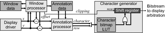
A more efficient approach is to represent the text directly as ASCII codes and interpret these on-the-fly to produce the bitmaps that need to be displayed. Character generation logic is simplified if character locations are restricted to a grid, but more general positioning can be accommodated. The process is outlined in Figure 12.12. The display driver produces the position of the current pixel being displayed. The window processor receives this and, based on which window is currently visible at that location (if any), selects the annotation data associated with the window and then provides the offset based on window position and character generation latency for the annotation processor. The annotation processor then detects the leading edge of each character and outputs the ASCII code and row within the character to the character generator. The line of pixels is read from the character generator bitmap and is ORed into the output shift register, combining it with any other characters that are also being produced. The shift register shifts the bits out sequentially, producing the character glyph on the display. The window processor detects the trailing edge of the window and resets the shift register at the appropriate time to clip the character to within the window borders. Of course, there are many more details that have been skipped within this simplified explanation (Buhler, 2007).
Figure 12.12 Character generation process.
12.2.2.4 Arbitration Issues
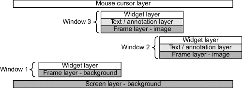
With several processes producing output for the display, it is essential to combine these together appropriately. A relatively simple priority stack can be used to determine which process produces the pixel for the display, as illustrated in Figure 12.13. The window processing determines which window and associated components are being displayed at any location. If no window is at the current pixel, then the background is displayed by default. Within a window, the background or image if it is an image window is the next layer. On top of this comes any textual annotation and widgets. At the highest priority is the mouse cursor layer. Any object on a higher priority layer will either mask (or modify) the underlying layers.
Figure 12.13 Window layering showing the arbitration priority. (Reproduced with permission from D.G. Bailey et al., “GATEOS: A windowing operating system for FPGAs,” IEEE International Workshop on Electronic Design Test and Applications, 405–409, 2006. © 2006 IEEE.)
Many peripheral devices communicate using some form of serial communications. This section briefly describes the most common of these, along with related FPGA implementation issues.
12.3.1 PS2 Interface
The PS2 is a low speed serial connection designed primarily for communication between a computer and keyboard or mouse. Since the PS2 protocol is much easier to work with than the more modern USB standard, it has become the method of choice for connecting a mouse or keyboard directly to an FPGA. Since the underlying PS2 protocol is the same for both the keyboard and mouse (Chapweske, 2003), it is described first. The specific communication is then described for interfacing with a mouse and keyboard.
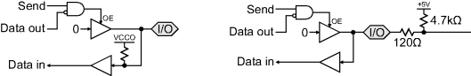
The PS2 connector provides a 5 Volt supply to power the keyboard or mouse and also has data and clock signals. The data and clock signals use an open collector interface. These can be implemented on the FPGA by using tristate output control to drive the output pin low when needed and use an internal pull-up resistor on the input to pull the signal to its default high state (Figure 12.14). If the pull-up voltage is too low, or the pull-up resistor is too strong, then an external pull-up resistor may be used.
Figure 12.14 Implementation of an open collector or passive pull-up data bus. Left: using an internal pull-up resistor; right: with external pull-up resistor.
Both the clock and data signals are only driven when transferring data; in the idle state, both lines are at their default high state. The clock signal (typically 10–16 kHz) is always generated by the PS2 device, so if the FPGA wants to send a command to the device it must signal with a request to send (RTS) pattern. This consists of pulling the clock signal low for at least 100 microseconds, then pulling the data signal low and releasing the clock. This instructs the device to begin transmitting a clock enabling the FPGA to transmit data.
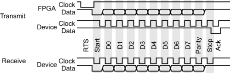
Each packet, whether transmitting or receiving, consists of 11 clock cycles from the device (Figure 12.15):
- a start bit, which is always low (the RTS from the FPGA provides the initial start bit for FPGA to device communication);
- eight data bits, sent least significant bit first;
- a parity bit, using odd parity (the number of ones in the data bits plus parity bit is odd);
- a stop bit, which is always high;
- and a final acknowledge bit, sent by the device only when the FPGA is transmitting data to the device.
When the FPGA is transmitting data to the keyboard or mouse, the data line should be changed while the clock signal is low and be held while the clock is high. When receiving data from the device, the opposite occurs: the data changes while the clock is high and can be read on the falling edge of the clock.
Figure 12.15 PS2 communication sequences. Top: transmission from FPGA to device; bottom: receiving from the device.
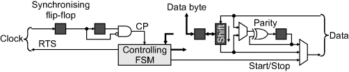
On the FPGA, the communication can be managed by a simple state machine; a skeleton implementation is given in Figure 12.16. The main control comes from the clock input from the device. A synchronising flip-flop is required to prevent metastability problems on the input (it is not needed on the data line because it is synchronous with the clock). The AND gate then detects the falling edge and produces a single pulse used to enable the finite state machine and the rest of the circuit through the clock enable pins on appropriate registers. This enables the driver to be operated in the main clock domain that is directly using the data. For transmit, the length of the RTS pulse may be determined by a counter. On the data side, a single shift register can be used to clock data in and out, with a single parity generator/checker switched between the input or the output. The output multiplexer selects the source of the current output bit. The state machine also has control inputs from the input data line (for checking start and stop bits) and from the parity checker.
Figure 12.16 Skeleton implementation for a PS2 driver.
12.3.1.1 Mouse
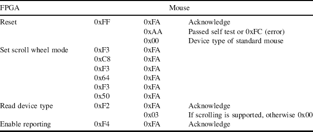
To use the mouse, the FPGA must first confirm that a mouse is connected to the PS2 port. This consists of sending a sequence of commands to the mouse and checking the response. A selection of the main commands is listed in Table 12.2. The mouse may be operated in one of several modes, the most useful of which is probably the streaming mode, where the mouse reports any changes in position or button status. If the mouse has a scroll wheel, it may also be enabled by sending the appropriate sequence.
Table 12.2 Main mouse commands and responses.
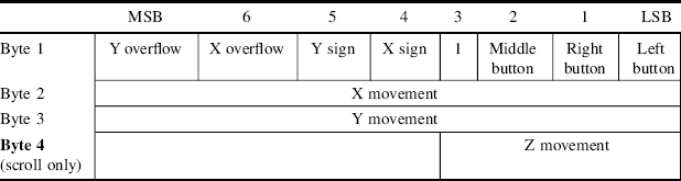
When in streaming mode, whenever the mouse is moved or a button is pressed or released the mouse streams three byte packets, as listed in Table 12.3. If the mouse has been successfully put into scroll wheel mode (device type reports as 0x03), the data packet is four bytes long. The movements are all relative to the previously reported position, with the X and Y movements represented using 9-bit two's complement offsets. If the offset exceeds ±255 then the corresponding overflow bit is set. The scroll wheel movement is a 4-bit two's complement offset, contained in the fourth byte.
Table 12.3 Mouse data packet in streaming mode.
12.3.1.2 Keyboard
A keyboard is detected by sending a reset command to the PS2 port. After the self test response is received, sending a read device type command (Table 12.2) should result in a two-byte device type of 0xAB, 0x83.
Whenever a key is pressed, the corresponding scan code (listed in Figure 12.17) is transmitted by the keyboard to the host. While the key is held down, the keyboard will periodically resend the scan code. When the key is released, a key-up scan code is sent, which for one-byte codes consists of 0xF0 followed by the scan code, and for two-byte codes, the 0xF0 comes after the 0xE0. The keyboard does not take into account whether or not the Ctrl, Shift or Alt keys are down – it is the responsibility of the host to account for these when interpreting the scan codes. If ASCII input is required, these scan codes may be converted to ASCII using a lookup table, combined with the shift status.
Figure 12.17 Keyboard scan-code numbers in hexadecimal. (1) E0 12 E0 7C; (2) E1 14 77.
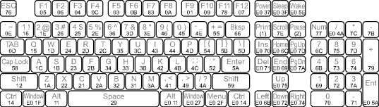
The indicator LEDs on the keyboard may be set by sending the command 0xED followed by a data byte with Scroll Lock in bit 0, Num Lock in bit 1 and Caps Lock in bit 2.
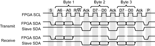
12.3.2 I2C
Many devices and interface chips are configured using an Inter IC (I2C) bus (NXP, 2007) or related communications protocol (for example, SMBus and PMBus used within computer systems). This is a two wire serial bus, with a data line (SDA) and clock line (SCL). Many devices may be connected on the single bus, including multiple bus masters, with each device on the bus individually addressable. The bus supports multiple data rates, from 100 kbit/s up to 3.4 Mbit/s, with the speed limited by the slowest device on the bus. When connecting to peripherals from an FPGA, it is assumed here that there is only a single bus master – the FPGA, and that it will be programmed to run at the speed of the slowest peripheral. (To handle the more complex case of multiple bus masters, consult the I2C specifications; NXP, 2007.)
The bus lines normally use a passive pull-up (like the PS2 port; Figure 12.14), although active pull-up may be used when operating with a single master and none of the devices will stretch the clock. The clock signal is always generated by the master, which also initiates and terminates any data transfer. Normally, the data signal is only allowed to change while the clock signal is low. The exception to this is indicating a start condition (S) or a stop condition (P). Each byte transferred requires nine clock cycles: eight to transfer data bits (MSB first) and one to acknowledge.
A transfer is initiated by the master (the FPGA) signalling a start condition: pulling SDA low while the clock is high. The first byte in any data transfer is always sent by the bus master and consists of the 7-bit address of the slave device and a ![]() bit. This is then acknowledged by the addressed slave pulling SDA low for the ninth clock cycle. The remainder of the transfer depends on whether the master signalled a read or a write (Figure 12.18). When the FPGA is writing, each byte transferred is acknowledged by the slave, unless there is some error condition (for example it was not able to understand a command that was sent). At the end of the transfer, the master signals a stop condition (a rising edge on SDA after the clock has gone high) or another start condition if it wishes to make another transfer. When reading from the device, after the first address byte the slave begins transmitting data which is acknowledged by the FPGA. After the last byte, the FPGA sends a negative acknowledgement followed by the stop or repeated start condition.
bit. This is then acknowledged by the addressed slave pulling SDA low for the ninth clock cycle. The remainder of the transfer depends on whether the master signalled a read or a write (Figure 12.18). When the FPGA is writing, each byte transferred is acknowledged by the slave, unless there is some error condition (for example it was not able to understand a command that was sent). At the end of the transfer, the master signals a stop condition (a rising edge on SDA after the clock has gone high) or another start condition if it wishes to make another transfer. When reading from the device, after the first address byte the slave begins transmitting data which is acknowledged by the FPGA. After the last byte, the FPGA sends a negative acknowledgement followed by the stop or repeated start condition.
Figure 12.18 I2C communication sequence. Top: writing to the device; bottom: reading.
There are four conditions that can lead to a negative acknowledgement (NXP, 2007), indicating that the transfer should be aborted:
- There was no slave on the bus with the specified address. Since there will be no response, the default will be for the bus to stay high.
- The slave device is not ready to communicate or cannot receive any more data from the master.
- The data sent to the slave was invalid, out of range or otherwise not understood by the slave.
- When the master is receiving data from a slave, to indicate that no more data should be transmitted.
Many I2C devices are register based, in that data is written to, or read from, a numbered register on the device. A write is straightforward – the FPGA sends the write to the slave, followed by the register address, then the data written to that register. Reading from a register is a little more involved. Firstly the FPGA needs to send a write to the slave and then write the register address. Then the FPGA sends a repeated start condition to terminate the first transaction and begin a new one. This consists of sending a read to the slave, and then the slave returns the contents of the register addressed in the first message.
An FPGA implementation of I2C is made easier by the FPGA being the bus master and providing the clock signal. The clock signal can be produced simply by dividing down the clock within the main clock domain. A finite state machine may be used to control the driver, using a circuit similar to Figure 12.16 (obviously the parity generator and checker are not required). The control is a little more complex as a result of slave addressing. However, the driver can be kept reasonably simple by separating the driver from the data interpretation.
12.3.3 SPI
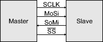
Another serial bus architecture is the serial peripheral interface (SPI). It is sometimes used with sensors and is commonly used as an interface to serial memories. It is both simpler and faster than I2C, although it has no formal protocols and there are several variations. The basic structure of the interface is as shown in Figure 12.19. The master selects the slave device and then data is communicated in synchronisation with the clock. To access multiple slaves, each slave requires its own separate slave select (![]() ) pin, although the clock and data lines can be shared. The data transfer is full duplex, with MoSi being the master output/slave input and SoMi the slave output/master input, although both lines do not always carry meaningful data simultaneously. The meaning of the data transferred, and even the size of the transfer, is dependent on the size of the device. Therefore, it is necessary to consult with the manufacturer's documentation on the specific commands and protocols used in order to design an appropriate driver for the peripheral.
) pin, although the clock and data lines can be shared. The data transfer is full duplex, with MoSi being the master output/slave input and SoMi the slave output/master input, although both lines do not always carry meaningful data simultaneously. The meaning of the data transferred, and even the size of the transfer, is dependent on the size of the device. Therefore, it is necessary to consult with the manufacturer's documentation on the specific commands and protocols used in order to design an appropriate driver for the peripheral.
Figure 12.19 Serial peripheral interface.
Within an FPGA-based system, an SPI interface can be used to provide the configuration data for the FPGA. The application may require access to the SPI bus if the application has the ability to reprogram the configuration memory. It may also provide other non-volatile data storage as required by the particular application.
12.3.4 RS-232
Another common serial interface is RS-232. While in many applications it has been superseded by USB, it still remains popular because of its simplicity and is a standard peripheral in many microcontroller chips. While technically RS-232 refers to the particular electrical signalling standard, it is often uses synonymously for asynchronous serial communication, and this is primarily the sense used here. To convert from normal logic levels to RS-232 levels, an appropriate interface chip is used, for example the MAX232 from Maxim Integrated Products. The need for a common ground limits the length of an RS-232 cable. In an industrial setting, the differential signalling of RS-422 (or RS-485 for multidrop) are more robust.
Asynchronous communication is so-named because it does not use a clock signal. Before transmission, the data line is held in an idle state, (a logical 1). Transmission is started by sending a start bit (logic 0); the falling edge is used to synchronise the receiver to the transmitter. Following the start bit, five to eight data bits are sent, followed by an optional parity bit, and finally one to two stop bits (logic 1) which are used to synchronise with the next word transmitted. The following timing and data framing parameters must be agreed between the transmitter and receiver before transmission:
- the clock frequency;
- the number of data bits and the order in which they are sent (MSB or LSB first);
- whether to use a parity bit and, if so, whether odd or even parity is used;
- the number of stop bits (the minimum time before a new transmission may begin).
A half-duplex connection uses a single data line for both transmitting and receiving. This requires hardware handshaking to control the direction of the data transfer. The handshaking is asymmetric, using separate signal lines. One end is designated as a data terminal and it signals its desire to transmit by setting the request to send (RTS) signal low. This is acknowledged by a reply on the clear to send (CTS) line. Full-duplex uses separate independent data lines for transmitting and receiving.
The implementation of asynchronous communication with a predefined set of parameters is a straight forward extension of the circuit of Figure 12.16. However, being able to change the parameters at run-time makes the system significantly more complex.
12.3.5 USB
As mentioned earlier, interfacing to devices using USB is quite complex. For simple serial communication, the simplest approach is to connect to an integrated USB chip that enables asynchronous serial data to be streamed directly to it. Many such devices have a built-in microcontroller which manages the details of the USB protocols. The alternative is to use a soft-core processor on the FPGA to manage the communication and protocols. It is generally not worth the effort interfacing hardware directly to a USB connection.
12.3.6 Ethernet
The use of high speed Ethernet was introduced earlier in this chapter with the GigE Vision camera interface protocol. To recap, the communication interface requires a PHY for managing the physical signalling and a MAC core for encapsulating the data with the required Ethernet headers and controlling data transmission and reception. The use of Ethernet for point-to-point communication is relatively straightforward, although writing a driver for interfacing between the rest of the design and the Ethernet is not for the faint-hearted. Fortunately, logic cores are available to do most of the hard work.
Using an Ethernet connection to connect to the Internet adds a whole new layer of complexity. Communication on the Internet is based on the TCP/IP protocol. This is, in fact, a suite or stack of protocols (Roberts, 1996), where the Internet protocol (IP) encapsulates data transmitted with a header that describes the particular protocol, which is then transmitted (as payload) over Ethernet. Several of the core protocols of the Internet protocol suite are:
- The transmission control protocol (TCP) is one of the most commonly used IP protocols for the transmission of data on the Internet. It establishes and maintains a virtual stream connection between the two hosts, on which reliable bidirectional transfer of data may take place. The protocol has mechanisms for detecting dropped or corrupted packets and automatically retransmitting the data until it is received correctly.
- The user datagram protocol (UDP) provides a lightweight mechanism for the transmission of data packets from one host to another. While there is a checksum for checking data integrity, there is no mechanism for ensuring reliable delivery. UDP is used for time sensitive applications where the overhead of retransmitting lost or missing data is unacceptable, for example streamed media.
- The Internet control message protocol (ICMP) works behind the scenes to communicate status and error messages between hosts and routers in an Internet-based network.
- The address resolution protocol (ARP) maps an IP address to an Ethernet address to enable the packet to be sent to the correct destination on an Ethernet-based network.
On top of UDP and TCP are the application layer protocols, which specify how the actual data content is transferred for a particular application, such as file transfer, mail, news, domain name resolution, Web (HTTP), and so on.
While all of these component protocols could be implemented in hardware (Dollas et al., 2005), the complexity of the layered architecture can quickly become unwieldy. Consequently, the Internet protocol is probably best managed by a software-based protocol stack, with the Ethernet MAC implemented in hardware using the FPGA logic.
As outlined in Section 4.3.3, one advantage of equipping an embedded system with a full TCP/IP stack is that it provides a generic mechanism for remote communication. A Web interface allows remote control and setting of algorithm parameters. The results, including images, can be readily displayed directly through a Web interface. An Internet connection also allows the FPGA configuration to be remotely updated, providing a ready path for upgrades.
12.3.7 PCI Express
PCI express is the latest standard for connecting to peripherals within a high speed computer system (Wilen et al., 2003). Previous generations of the peripheral component interconnect (PCI) bus were parallel, with 32 or 64 data lines. However, as the bus speed is increased, two problems are encountered: increased cross-talk from the coupling between adjacent signal lines and increased skew between data lines resulting from small differences in path length. In switching to a serial connection, PCI express solves the skew problem (although a much higher clock rate is required to maintain the bandwidth) and uses differential signalling to significantly reduce the effects of cross-talk. The other significant change is that while PCI is a bus, shared by all peripherals, PCI express is a point-to-point connection with separate transmit and receive, avoiding overheads associated with bus arbitration and contention.
Each differential pair operates at 2.525 GBit/s, with a transmit and receive pair called a lane. Clocking is embedded within the signal by using 10 bits to encode each eight bits of data. This limits the length of consecutive zeros or ones to provide edges for a phase locked loop to recover the clock. (The new PCI express version 3 achieves the same effect with reduced overhead by scrambling the data first and using 130 bits to encode each 128 bits of data.) Higher bandwidth connections can run multiple lanes in parallel, with successive bytes sent down successive lanes.
At the link layer, additional overheads are introduced for CRC-based error detection and packet acknowledgements. Each data packet is kept in the transmit buffer until acknowledgement is received. This allows packets signalled as corrupt to be automatically resent.
Higher layers of the protocol create virtual links between the components that share the underlying physical link. This is implemented through a transaction layer, where each transaction consists of a request followed by a response. Between the request and response, the link is available for other traffic. Flow control uses a credit-based scheme where the receiver advertises the space available within the receive buffer as credit. The transmitter keeps track of its remaining credit and must stop transmitting before the buffer is full. As the receiver processes data and removes it from the buffer, it restores credit to the transmitting device.
PCI express is most commonly used to interface between an FPGA board and its host computer system, enabling the rapid transfer of data in high performance computing applications. Recent FPGAs have built in PCI express ports, with logic cores available for interfacing between the rest of the logic of the application.
In many applications, it is necessary to use memory external to the FPGA for frame buffers and other large memory blocks. External memory is also required when running an embedded processor with an operating system such as Linux. There are two main types of memory: static and dynamic. The issues involved in interfacing with these are described in turn.
A common issue, particularly with high speed memories (in particular DDR memories) is ensuring that any signal skew in the parallel data and address lines does not violate setup and hold times.
12.4.1 Static RAM
Static memory stores each bit using a latch. Each memory bit therefore requires a minimum of four transistors, with an additional two transistors used for accessing the latch for reading and writing. This is considerably larger than the one transistor used by dynamic memory, making it more expensive to manufacture. Its advantage is its speed, making it commonly used for intermediate memory sizes (in the low megabyte range), such as commonly used by cache memories in high end computer systems.
Almost all high speed synchronous memories are pipelined. Therefore, when reading, the data is available several clock cycles after the address is provided, although the memory has a throughput of one memory access per clock cycle. This access latency must be built into the design of the application. This makes external memories a little more difficult to use than internal block RAMs.
Usually when writing, both the address and data must be applied at the same time. Consequently, when following a read by a write, there is a dead time to allow the read to complete before the data pins are available for providing the data to be written. If using such memories in a design, this dead time must be taken into account in the timing budget. While such memories may be suitable for reading or writing large blocks, such as might be encountered when streaming an image to or from a frame buffer, they are unsuitable for two-phase designs, where reads and writes may be alternated.
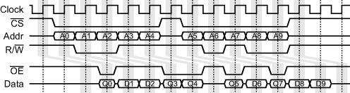
Zero bus turnaround (ZBT) memories have no dead period between writes and reads. This is accomplished by providing the data to be written after the address, as shown in Figure 12.20. The ability to switch between reads and writes from one cycle to the next makes ZBT memories significantly easier to interface to an application. The data to be written may be delayed within the FPGA if necessary by using a pipeline.
Figure 12.20 Typical timing for a pipelined ZBT static memory with two clock cycles latency.
12.4.2 Dynamic RAM
Dynamic memory, because of its lower cost, is best suited for larger volumes of memory. It uses a single transistor per memory cell, with the data stored as charge on a capacitor. Since the charge leaks off the capacitor, it must be refreshed at least once every 64 ms to prevent the data from being lost. To achieve this with large memories, dynamic memories are structured so that a complete row (within the two dimensional memory array) is refreshed at a time. The availability of a whole row at a time leads to a paged memory structure, where a row is selected first, and then the column within that row is read from or written to.
Interface to a chip is controlled through a sequence of commands which are provided through a set of control pins. A typical command sequence is as follows:
- An activate command selects the memory row to use. The address lines specify which row is selected. Activating a row reads the row into the column sense amplifiers, enabling the data within that row to be accessed. It also has the side effect of refreshing the charge on the capacitors within that row. Row activation typically takes several clock cycles.
- Once activated, read and write commands may be made to that row. With a read or write command, the address lines specify the column that is to be read or written. A read or write has several clock cycles latency, however these are pipelined, enabling one access per clock cycle to data on that row. When writing, the data must be provided with the address, so there is a bus turnaround delay when switching from reads to writes. Operating in burst mode enables several successive memory locations to be read or written with a single command. This is exploited with DDR memories, giving two reads or writes per clock cycle, one on each edge of the clock.
- Before selecting another memory row, it is necessary to close the row with a precharge command. This returns the sense amplifiers to an idle state ready to sense the next row.
- A refresh command refreshes one row of memory. An internal counter is maintained so that the rows are refreshed in sequence. The refresh command internally activates a row, waits for sufficient time for the charge on the capacitors to be refreshed, and then returns the line to the idle state. While it is possible to do this manually, having a refresh command simplifies the memory controller.
There is considerable latency, especially when moving from one row to another. To help alleviate this, most DRAM chips have multiple banks of memory internally, so that one bank may be used while waiting for row activation or precharging within another bank.
Reading or writing from a dynamic memory is, therefore, not a simple matter of providing the address and data. The complex sequence of operations to access a particular memory and ensure that the memory is kept refreshed requires a memory controller. Some new FPGAs incorporate dedicated hardware memory controllers to simplify access (Xilinx, 2010c). Otherwise it is necessary to build the memory controller from the fabric of the FPGA.
If using dynamic memory for a frame buffer, it works best with streaming mode because there will be many sequential accesses to the same row. Streamed access by columns (for example with the FFT) is generally not practical because of the large latencies to switch from one memory row to another. This may be overcome to some extent by creating a mapping between logical memory and physical memory to increase the number of sequential accesses to the same page. However, such techniques complicate the system design. A similar problem is encountered with random access processing. In such systems, it may be necessary to maintain a static memory as a frame buffer in addition to the dynamic memory. If the access pattern is known in advance, then a smaller cache may be built on the FPGA.
DIMMs (dual in line memory modules) consist of a number of dynamic RAM chips mounted on a printed circuit board to give a wider data width. These are commonly used with conventional computer systems, but can also be used with FPGAs.
12.4.3 Flash Memory
Flash memory is non-volatile, making it useful for storing data required by an application while the FPGA is switched off, or when switching from one configuration file to another. The basic mechanism is to have charge stored on a floating gate transistor, which results in a change in transistor threshold voltage, enabling the different states to be identified (Pavan et al., 1997). Programming consists of injecting charge onto the floating gate, while erasing removes the charge. There are two main types of flash memory based on how these transistors are arranged: NOR flash and NAND flash.
NOR flash is similar to regular memory, with address and data lines allowing individual transistors to be read or written using a random access memory pattern. Read access times are reasonably fast, although writes are very slow in comparison with static or dynamic memories, and this must be taken into account by the application. Erasure is on a block by block basis, and is also very slow. Erasing a block sets all the bits to ones, and writing can only change ones to zeros. To change a zero to a one requires erasing the complete block, losing any data contained within it.
NAND flash arranges the transistors differently to enable a higher packing density (resulting in lower cost). The consequence is that NAND flash has page or sector-based structure, making it better suited for sequential access than random access. Programming individual bytes and random access are difficult, but programming and erasing blocks is significantly faster than NOR flash (Micron, 2010). Internally, reading copies the whole block from non-volatile storage into buffer register (typically 25 µs) from which the data can then be streamed out (typically 25 ns per byte or word). Similarly, writing streams the data into the buffer register (25 ns per transfer) from which the whole block is programmed at once (200–500 µs). Since NAND flash memories are orientated to sequential access, the data pins are usually multiplexed to carry commands and the page address.
NAND flash requires error checking and correction to ensure data integrity. Each block usually has a number of spare bytes that can be used for storing error correction codes. However, it is up to the controller to implement any error checking and correction. It is also important to check the status after a program or erase operation to confirm that the operation has completed successfully. If not successful, such blocks should be marked as bad and not be used. Micron provides VHDL code that may be used for the basis of a NAND flash controller (Micron, 2007).
This chapter has reviewed some basic interfacing issues particularly related to embedded vision applications.
A camera or input sensor is perhaps the key peripheral in a vision system. The most straightforward approach is to interface directly with the sensor chip. This gives the lowest latency and avoids many of the complications of interfacing with the USB or Firewire connection of consumer cameras. An issue with CMOS sensors is characterising and correcting the distortions introduced by rolling shutter-based electronic shuttering. This is a complex problem that depends on the motion of both object and camera. When interfacing directly with a colour sensor, it is also necessary for the FPGA to recreate the full colour image by interpolating the values of the missing colour channels.
Image display is another important capability, even if it is just used for debugging and system tuning. A simple display is relatively easy to generate, although an analogue output will require external digital to analogue converters. A DVI output keeps the system all digital, although it will require more logic on the FPGA and high speed SERDES interfaces to produce the serial signals. Alternatively, a DVI transmitter chip offloads the logic at the expense of increased component count.
Some issues with display content generation have been discussed briefly. In particular, techniques for window and character generation have been outlined.
A range of serial communication protocols have been outlined. The control channel for many devices (including cameras and displays) is usually over a relatively low speed serial link. The slower speed makes the design easier, with simple interfaces able to be built with relatively few resources. Higher speed connections such as gigabit Ethernet and PCI express are significantly more complex and should be built using intellectual property blocks. While both will be less common in embedded vision applications, PCI express is commonly used to interface between a host computer system and an FPGA in a high performance reconfigurable computing platform.
Finally, issues with interfacing to external memories have been considered briefly. The main complication is the memory latency with pipelined access. This is particularly acute with dynamic memory, which requires a page be selected before it is accessed. Careful design of the system, and in particular the memory controller, is required to prevent the acceleration gained elsewhere in the algorithm from being lost due to memory bandwidth limitations.