
Chapter 3
Languages
In Chapter 2, a low level view of the architecture of FPGAs was presented. To programme an FPGA at this level, it is necessary to break down the design into the fine-grained logic blocks available on the FPGA and build up the logic required by the application from these blocks. There are two main problems with representing designs at this level. Firstly, designing at such a low level is both tedious and error prone. Secondly, the portability would be limited to FPGAs that had the same basic architecture and logic block granularity. While it is possible to programme FPGAs at this level, it is akin to programming a microprocessor in assembly language. It may be appropriate for the parts of the design where the timing and resource use are critical. However, for most applications, this is too low level, and this is also the case for most image processing designs based on FPGAs.
Fortunately, the tools for implementing algorithms and systems on FPGAs enable working at a higher level. Implementing a working design requires several key steps, as illustrated by the generic design flow in Figure 3.1. Firstly, the design must be coded in some human readable form. This represents the design using a hardware description language (HDL) and captures the essential aspects of the design that enables it to be both simulated and synthesised onto an FPGA. Design representation is the primary focus of this chapter. Although many HDLs are based on software languages, they are not software but instead describe the hardware required to implement the design. For an FPGA implementation of an algorithm it is necessary to describe not only the algorithm, but also the hardware used to implement it. Most development environments enable the hardware description to be ‘compiled’ and simulated at the logical level to verify that it behaves in the intended manner.
Figure 3.1 Steps to implementing a design on an FPGA.

Synthesis takes the logical representation describing the hardware and converts it to a device or gate level net-list representing the actual hardware that is to be constructed on the FPGA. This form defines the circuits in terms of basic building blocks, both at the logic gate level and in terms of the primitives available on the FPGA if they have been used within the description. It also defines the interconnectivity between the building blocks. For interchange between different tools, a net-list is often represented using EDIF (electronic design interchange format). Synthesis constraints control aspects of the synthesis process, such as whether to: optimise for speed or area; automatically extract and optimise finite state machines; force set and reset to operate synchronously; and so on. Gate level functional simulation verifies that the design has been synthesised correctly, and provides more information on the specific low level characteristics of the circuit than the higher level simulation.
The next stage is to map the net-list onto the target FGPA. There are two phases to this process. Mapping determines how the logic maps onto the specific components available on FPGA. In particular, this phase partitions the logic of the design into the LUTs, splitting complex logic over several LUTs, or merging logic to fit within a single LUT where appropriate. The place and route phase then associates these mapped components with particular logic blocks on the FPGA and determines the routing required to connect the logic blocks, memories and I/Os. Implementation constraints direct the placement of logic to specific blocks, in particular associating inputs and outputs with specified pins. They also specify the required timing, which is used to guide the placement and routing of critical nets. Once the design has been mapped onto the FPGA, more accurate estimates of the circuit timing are available based on the lengths of the connections, fan-outs and particular resources that are used to implement the logic function.
The final stage is to generate the configuration file required to programme the FPGA. During development, the configuration file can be loaded onto the target system to verify that the design works as intended and that it correctly interacts with the other components within the system. In the deployed system, the FPGA is programmed by automatically loading the configuration file from flash memory on power-on.
As can be seen from Figure 3.1, implementing a design on an FPGA is quite different from implementing a design in software, even on a processor within an embedded system. It requires a hardware mindset, even during the initial design. However, image processing is usually considered to be a software development task. Successful implementation of algorithms on an FPGA therefore requires a mix of both software (algorithmic) and hardware (logic circuit design) skills.
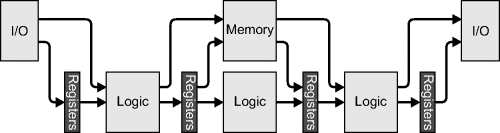
Most FPGA-based design is carried out at an intermediate level that is a mixture of both algorithmic and circuit level design. The implementation of synchronous systems is usually performed at the register transfer level (RTL). As illustrated in Figure 3.2, this structures the application as a series of alternating blocks of logic and registers. The structure is not necessarily linear, as implied by Figure 3.2; from a computational perspective, the primary purpose of each block of logic is to determine the next value that will be stored into the registers on its outputs. It can take its inputs from anywhere: other registers, I/O pins or internal memory blocks. As demonstrated in Figure 3.2, inputs, outputs and memory accesses may be either direct or via registers. The blocks of logic are not directly clocked; all of the clocking is through the registers (and also the memory if it is synchronous). Therefore, the signals must propagate through the logic before they can be clocked into the registers. This limits the clock speed of the design to the propagation delay through the most complex block.
Figure 3.2 Basic structure of any application – logic interspersed with registers.
The art of implementing an algorithm on an FPGA therefore falls to decomposing the algorithm into a sequence of register transfers, and determining the appropriate logic between each register. Note that, unlike implementing algorithms in software, each logic block operates in parallel. This usually requires adapting the algorithm from a conventional sequential form into one that can exploit the parallelism available from hardware.
Implicit within Figure 3.2 is the control logic required to sequence the steps within the algorithm. Depending on the algorithm and its implementation, not all of the registers may necessarily be updated at every clock cycle. This can be achieved by using the clock enable for the registers to control when they are updated. Also, the computation to produce a value for a register may not necessarily be the same every cycle. This requires a multiplexer on the inputs of the registers to select the appropriate computation depending on the current stage within the algorithm. These are made more explicit in Figure 3.3, with control logic providing the clock enable and multiplexer selection signals. Implicit within the compute logic are any memory elements that may be used to perform part of the computation, or provide cached input or output data.
Figure 3.3 A rearrangement of Figure 3.2 to explicitly separate the control and compute logic.
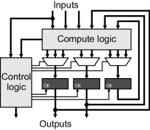
The distinction between control logic and compute logic can help with the transition from an algorithm to hardware. The control logic determines what is computed (or more precisely which computation gets saved in which register – in hardware, the logic is always adjusting its output to reflect changes on its inputs), while the compute logic actually performs the computation.
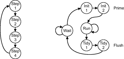
Since the computation is often context dependent, a common implementation of the control logic is as a finite state machine, with the context encoded in the states. Figure 3.4 gives two examples of simple finite state machines. The one on the left illustrates how a sequential algorithm may be implemented on parallel hardware. The algorithm consists of four steps, each of which take exactly one clock cycle, and when the algorithm has completed the fourth step, it returns to the start (perhaps operating on the next data item). The finite state machine on the right represents the typical structure for the control for a three-stage pipelined stream process with one clock cycle per pixel. The algorithm begins in the Wait state, waiting for the first pixel. When the first pixel arrives, the next two states are initialisation, priming the processing pipeline. Once primed, the pipeline stays within the Run state while pixel data is arriving. At the end of each block of data, the state machine transitions to the Tidy states where the pipeline is flushed, completing the calculations for the last pixels to arrive. It then returns to the Wait state, waiting for the first pixel on the next block.
Figure 3.4 Example finite state machines. Left: a repeating sequential process; right: a pipelined stream process.
The transitions from one state to the next may be determined by input (control) signals or, for more complex algorithms, determined by the data being processed, as reflected in Figure 3.3. In practise, an algorithm is decomposed into a series of modules. Rather than control everything with a single large finite state machine, the control logic is also modularised, with a separate state machine for each module.
Having looked at the basic structure of an algorithm when implemented on an FPGA, the next step is to look at the representation of the algorithm being programmed onto the FPGA.
3.1 Hardware Description Languages
The traditional approach to describing electronic circuits is through schematic diagrams. These provide a graphical representation of the components and connectivity. They are best used for representing smaller designs at the transistor and gate level. For higher level designs, they represent modules and packages as block diagrams. Modern schematic capture tools integrate circuit simulation and printed circuit board layout, making them invaluable for the production of physical systems. High end tools also integrate hardware description languages allowing the complete development and modelling of systems containing FPGAs and other programmable hardware. However, the level of abstraction of schematic diagrams is typically too low for representing complex algorithmic designs. At the lowest level, they can represent logic circuits as transistors and logic gates. At the register transfer level, a schematic representation is structural, as a collection of components or block diagram, rather than clearly representing the behaviour or algorithm. This makes them difficult to navigate for algorithmic designs, because the behaviour is not particularly transparent from a structural representation.
From these roots, hardware description languages evolved in the 1980s to address some of the limitations and shortcomings of schematic representations, and to provide a standard representation of the behaviour of a circuit. Since hardware is inherently parallel, it is necessary for an HDL to be able to specify and model concurrent behaviour down to the logic gate level. This makes HDLs quite different from conventional software languages, which are primarily sequential.
The two main HDLs are VHDL (very high speed integrated circuit HDL) and Verilog, both of which have since been made into IEEE standards (the current standards are IEEE, 2009, 2006a, respectively). Their original purpose was for documenting and modelling electronic systems. Both are hierarchical structural languages in that they describe the hardware structurally in terms of logic blocks and their interconnections. They also allow a behavioural description of the functionality of the circuit, rather than necessarily having to specifically identify the logic circuits. A behavioural description, as its name implies, describes how the circuit is to behave, or respond to changes on its inputs. It is, therefore, the role of the synthesis tools to determine the actual logic required to implement the specified behaviour.
The primary focus of VHDL and Verilog is for verification and simulation of logic circuits. Therefore, modules can readily be written in either language for testing the functionality of the circuits described. Through the design of appropriate test benches, this allows the design to be thoroughly tested for correctness before it is synthesised. The complexity of synthesising a circuit from its behavioural description limits what can be synthesised. Structural designs can be readily synthesised, as can behavioural descriptions that conform to an RTL coding style. However, these restrictions mean that many of the constructs available within both languages are not synthesisable.
3.1.1.1 VHDL
VHDL has its roots in the US Department of Defence and was built on the Ada language. VHDL therefore inherits many of the characteristics of Ada, including being strongly typed and having a tendency to be somewhat verbose. The synthesisable subset of VHDL is specified in (IEEE, 2004).
Perhaps the best way to briefly describe the language is to demonstrate its functionality through a simple example. This will implement the recursive streamed filter with input I and output Q:
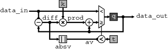
where k and t are constants. The corresponding schematic for this is shown in Figure 3.5. One VHDL representation of this is given in Listing 3.1.
Figure 3.5 Schematic representation of Equation 3.1.
Listing 3.1 VHDL implementation of the filter illustrated in Figure 3.5
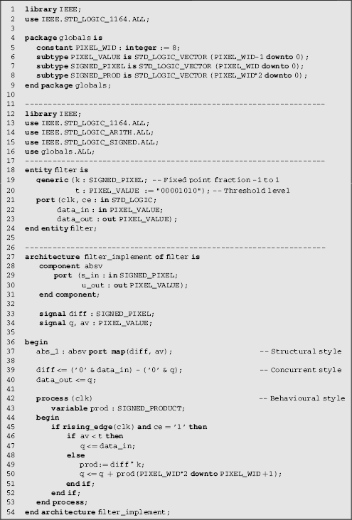
The main features of VHDL will be demonstrated through a line-by-line explanation of the code in Listing 3.1. The first two lines indicate that the following code will make use of definitions from within the STD_LOGIC_1164 package within the IEEE library. The basic representation of a single bit wire is STD_LOGIC, which can represent not only logic 0 and 1, but a range of other levels as well including a weak high or low, high impedance, and undefined. When synthesised, this will be either 0 or 1 (or high impedance if the output of a tristate buffer), but the other states are useful for detecting errors during simulation. A multi-bit number is represented by the type STD_LOGIC_VECTOR.
Since VHDL is strongly typed, the types of every operand and the result to which it is assigned must match exactly; any mismatch will result in a compiler error. This helps to ensure the correctness and internal consistency of the specification, but does mean that the developer has to do extra work to make everything match. To simplify this, a package is defined in lines 4–9, which defines the width of a pixel, and a number of types used within the project. Normally the package will be in a separate file and be used by all of the files within the project, effectively centralising the definitions. In this case it is included within the same file for compactness.
Lines 12–16 list the packages that will be used in the following definitions. The STD_LOGIC_ARITH overloads the definitions of arithmetic operations for the STD_LOGIC_VECTOR types, and these are extended in STD_LOGIC_SIGNED for signed arithmetic. Line 16 includes the package containing our type definitions.
Every block within VHDL consists of two parts: an entity (lines 18–24), which defines the block and its interfaces, and an architecture (lines 27–54), which describes the implementation. Within the entity, generic defines parameters of the entity – in this case the filter gain and threshold value. The threshold t is given a default value of 10. Rather than enter the value as a bit string, the conversion function CONV_TO_STD_LOGIC_VECTOR() defined in STD_LOGIC_ARITH can be used. A value needs to be given for k when the filter is instantiated and, if a value is given for t, it will override the default. Making them generic generalises the code. The port defines all of the data connections for the block. Here, a clock and clock enable signals are required to control the register internal to the filter. The data input and output are defined as PIXEL_VALUE, making use of the previously defined type. Note that the generic items must be constants; if they are to be controlled by other logic they need to be specified within the port list to enable them to be connected with whatever is controlling their value. The entity definition contains all that is required to connect the filter to other components within the design.
The architecture block defines the implementation of the entity. An entity may have several architectures associated with it, each describing a different implementation. The head of the architecture block defines the components and signals used within the architecture. A component is any other external entity that will be instantiated within the body of the architecture. In the example here, lines 28–31 define the absolute value block in Figure 3.5, which is going to be instantiated by another VHDL entity called absv. Lines 33 and 34 define the signals used within this implementation; these are labels for any internal wires or registers. The names here correspond to the labels within Figure 3.5.
There are three distinct coding styles that can be used within the body of an architecture. The first style is a structural style. This builds up a design by instantiating and connecting a number of component blocks. On line 37, an instance of the absv component called abs_1 is incorporated into the design. The port map defines the connections to the component instance; here diff is connected to the s_in port and av to the u_out output. A purely structural implementation would describe everything in this manner, using a hierarchy of connected components in much the same way that the schematic diagram would represent the circuit. More complex structural implementations can use generate statements and loops to instantiate multiple copies of a component for example to build multi-bit circuits from single bit components.
The second programming style is illustrated in lines 39 and 40. It places more focus on the flow of data through the block, and describes the implementation in terms of concurrent signal assignments. Whenever any of the signals on the right hand side changes, the corresponding statement is evaluated with the result immediately assigned to the left hand side. Line 39 subtracts q from data_in to produce the signal labelled diff. It is necessary to concatenate a 0 bit to the front of each of the terms to be able to represent the sign of the result. Line 40 connects the output port of the filter to the output of the register.
The third programming style defines the implementation in terms of its behaviour through one or more process statements. Each process block is executed whenever any of the signals within its sensitivity list changes. The process on lines 42 to 53 will be executed whenever clk changes. The statements within a process block are executed sequentially, making it a little more like a conventional programming language. If written in an RTL style, such a behavioural description can be converted to the corresponding logic by the synthesis tools. Within the header, any variables used within the process are defined. A variable is a little like a signal, with the difference being that an assignment to a variable takes place immediately within the process, whereas any assignment to signals is made whenever a wait statement or the end of the process is reached. At that point, all signal assignments within the process are made concurrently; up to that point, all signals will have the value when execution of the process started. That is variable assignments are made sequentially, whereas signal assignments are concurrent.
The if statement on line 45 specifies that the enclosed statements are only executed on the rising edge of the clock when the clock enable is set (the rising_edge function is defined in STD_LOGIC_1164). Consequently, any signal assignments within this block will be synchronous, implying that a register is required. The if on lines 46 to 51 imply a multiplexer, with each branch providing an appropriate input for the signal (register) q. Line 49 performs the multiplication and assigns the result to the variable prod. The multiplication operation is defined in STD_LOGIC_SIGNED to perform a signed multiplication, producing a full precision output. The least significant bits are truncated and the result accumulated in q in line 50.
As can be seen, the different programming styles may be mixed within any given design. All statements within the architecture are executed concurrently, in the sense that whenever any of the inputs change, the corresponding statement is evaluated.
While this example illustrates many of the features and characteristics of VHDL, it is by no means exhaustive. The interested reader should consult the standard (IEEE, 2004; 2009), the documentation for their synthesis tool or other references on VHDL (for example Bhasker, 1999; Ashenden, 2008).
3.1.1.2 Verilog
Verilog has many of the same features as VHDL. However, in contrast with VHDL which has its roots in Ada, Verilog is loosely modelled after C. Consequently, Verilog is more compact that VHDL. Again, as primarily a modelling language, not all language constructs are synthesisable (IEEE, 2005).
Each block within a design is specified as a module, with associated input and output ports. A structural design defines its operation by referencing lower level modules, and describes the interconnections between the module instances.
Within the module, there are two types of variables: wire and reg. A wire is as it sounds, a wire, while a reg is a variable that holds its value until it is changed (this is often, but not necessarily, associated with a flip-flop). Wider variables are created as arrays of bits. An assign statement performs continuous assignment. Whenever any variable on the right hand side of such a statement changes, the assignment is evaluated to determine the new value for the left hand side. The assignments are effectively all concurrent; the order that they appear within the module is immaterial.
An initial block contains sequential statements, with the block executing once on initialisation. An always block similarly executes a block of sequential statements whenever one of the variables in its sensitivity list changes. Within such blocks, there are two types of assignment: sequential, where the left hand side is updated immediately; and concurrent which waits until the next time unit or clock cycle, when all such assignments are made in parallel.
As with VHDL, a range of programming styles may be used. A full description of Verilog is beyond the scope of this book. The interested reader is referred to the standards (IEEE, 2005; 2006a) or other language references (for example Bhasker, 2005).
3.1.1.3 Summary
Standard HDLs are very good at describing the structure of a hardware design. Structural descriptions generally give the best performance, using the minimum of resources (if optimised appropriately by the designer). This makes them good for developing libraries of intellectual property (IP) blocks that may be instantiated many times or in many designs. However, design at the structural level is quite low level and can be very tedious. At a higher level, HDLs can model functionality through a behavioural specification. This describes what the circuit does, without necessarily specifying how it is to be implemented. Consequently, the designer generally has less control, so although the design is at a higher level, it is relying on the synthesis tools to derive an efficient implementation. Only the subset of behavioural descriptions that conform to an RTL style is synthesisable.
The low level of HDLs makes exploration of the design space (the trade-offs between area, speed, latency and throughput) more difficult. It is time consuming enough to programme one design, let alone several different designs to investigate the effects of different levels of loop unrolling and pipelining.
HDLs, by necessity, are general purpose and allow considerable control over how the circuit is implemented. This is both an advantage and a disadvantage. The advantage is that the developer can target specific structures available on the FPGA, or optimise the design for speed or resources required by programming in particular ways. By giving the designer control over every aspect of the design, fast and efficient designs are possible. The disadvantage is that the designer must control everything in quite fine detail, including both the data and control flows. The flexibility comes from the relatively low-level constructs, but programming at this level requires a lot of basic bookkeeping. This makes complex algorithmic programming more difficult.
The low level of programming is also not always particularly transparent. Very similar behavioural constructs map to latches or multiplexers. While a structural design can specify registers explicitly, they tend to be implicit in the behavioural programming style. These characteristics require close attention be paid at the low level, and has a strong focus on the hardware rather than the algorithm. Compared to software-based languages, HDLs are a lot like programming in assembly language.
In an attempt to overcome this problem, over the last fifteen years considerable research has gone into the synthesis of hardware from high level languages, in particular from C. The rationale behind this is twofold. Firstly, it enables existing software to be easily ported or recompiled to a hardware implementation. Many algorithmic designs are first developed and tested using C or MATLAB®. Once working, the design is then often re-entered manually into an HDL after which it is necessary to verify and refine the design manually. This process is both time consuming and error-prone. Having a single source that can be compiled to both hardware and software would speed the development process considerably. It would also enable the partitioning of the final implementation between hardware and software to be explored more easily. The time critical and easily parallelisable components can be compiled to hardware, with the more sequential components compiled as software. A second motivation is to raise the level of abstraction to make hardware design more like software design, making it more accessible to software engineers (Alston and Madahar, 2002).
Unfortunately, there are significant differences between hardware and software that pose significant challenges to describing a hardware implementation using a software language. Five areas of difference identified by Edwards,) are concurrency, having a model of time, data types, memory model and communication patterns.
Hardware is inherently concurrent, with each step or computation performed by separate hardware. In contrast, software performs its computation by reusing a central processor, making software inherently serial. As indicated in Chapter 1, software processors introduce parallelism at a range of levels: at the instruction level through wide instruction words (effectively issuing several instructions in parallel), temporally, through instruction pipelining (with successive instructions overlapping by being in different phases of the fetch/decode/execute cycle), through to coarse grained parallelism introduced by splitting the application into several relatively independent processes and using a separate thread for each. The fine-grained parallelism at the instruction level is closer to that of hardware, but is controlled by the particular architecture of the processor. The compiler just needs to map the high level statements to the given processing architecture. At this level the algorithm is primarily sequential, although compilers can (and do) exploit dependencies between instructions to maximise parallelism. At the thread or process level, the coarse-grained model does not match the fine-grained concurrency of hardware, but maps closer to having separate blocks of hardware for each thread or process.
Time and timing is absent from most software programming models. The sequential processing model of software ensures causality within an instruction sequence (Edwards, 2006), although this becomes more complex and less deterministic with multithreaded execution and task switching. However, the time taken for each task is not considered by the language. In contrast, hardware, and especially synchronous hardware, is often governed by strict timing constraints. Many hardware interactions must be controlled at the clock level and representing these with a high level software language can be difficult.
The data word width of a hardware system is usually optimised to the specific task being performed. In contrast, software languages have fixed word widths (8, 16, 32, 64 bits) related more to the underlying architecture than the computation being performed. Two approaches to this are to modify the language to allow the word width to be explicitly specified, or to make use of the object orientated features (Java or C++) to define new types and associated operators. Virtually all software languages support floating-point computation, and floating-point numbers have been the mainstay of scientific computing, including image and signal processing, for some time. However, until recently floating-point number representations have been avoided on FPGAs because of the cost of implementing the more complex hardware. It is only with higher capacity FPGAs and higher level languages that floating-point calculations have become practical in hardware for other than very specialised tasks.
The memory model of software is very different to that used within hardware systems. Software treats memory as a single large block. The compiler may map some local variables to registers, but the software model has everything stored in memory. This allows memory to be allocated to a process dynamically, with the associated memory block referenced by its address. C even allows efficient memory traversal algorithms through pointer arithmetic. In hardware, many local variables are not implemented in memory, but directly as registers. Memory is often fragmented into a large number of small, independent blocks. In such an environment, pointers have very little meaning, and dynamic allocation of memory resources is difficult, if not impossible. This has a direct impact on the algorithms that can readily be used or compiled to hardware.
The differences in memory structure also directly impact communication mechanisms between parallel processes. Software generally uses shared memory (including mailboxes) to communicate between processes. Such a model is sensible where there is only a single CPU (or small number of CPUs), and the processes cannot communicate directly. In hardware systems, parallel processes are truly concurrent and can therefore communicate directly. In data-synchronous systems, such as streamed pipelining, communication is often implicit, or through simple token passing. More complex systems can use FIFO buffers or other synchronising and communication mechanisms. In many hardware systems, the communication relies on dedicated hardware. This is particularly the case when communicating between clock domains.
Another major difference between hardware and software relates to the representation and execution of an algorithm. In software, an algorithm is represented as a sequence of instructions, stored in memory. A program counter points to the current instruction in memory, and a memory-based stack can be used to maintain state information, including any local variables. This allows algorithms to be implemented using recursion where within a procedure the state can be saved and the procedure called again. In hardware, the algorithm is represented by physical hardware connections. Saving the current algorithm state is difficult, making recursive algorithms impractical in hardware. Any such recursion within an algorithm must be remapped to iteration to allow a practical implementation.
In spite of these significant differences, three approaches have been used to develop synthesis tools from high level languages. One is to use the host language to create and manipulate a structural representation of the circuit constructed. This is effectively using the high level language to simply model the hardware, rather than directly specifying it. The second is to modify or extend the syntax of a high level language to provide constructs that enable it to be used to describe hardware (Todman et al., 2005; Edwards, 2006). The third approach is to use a standard high level language and requires the compiler to automatically extract parallelism from the design and appropriately map it to hardware. These three approaches are described in more detail with some examples of each of these approaches. Much of the literature reports experimental work, although there are now several commercial offerings.
3.2.1 Structural Approaches
Structural approaches work at describing the design using a structural model, rather than algorithmically. These are primarily tools that mimic the structural designs of conventional HDLs but within a standard programming language making the language and design more accessible to software engineers. They are able to use the programming constructs of the host language to automate some design tasks, or to facilitate parameterisation more naturally than standard HDLs. The other advantage of using a high level language is that it more readily enables targeting the result to either software or hardware, facilitating the partitioning of the design.
3.2.1.1 JHDL
JHDL (Bellows and Hutchings, 1998; Hutchings et al., 1999) is a Java-based hardware description language developed by the Configurable Computing Laboratory at the Brigham Young University. It began as a tool to experiment with run-time reconfigurability (Bellows and Hutchings, 2001) and was extended to synthesise the designs, targeting Xilinx FPGAs. It is based on a structural design, which is described programmatically using Java, with sets of classes representing objects, and wires. The integrated environment then allows the circuits to be simulated to verify and debug operation. Tools within the environment allow the manipulation of the design, including the placing of components on the FPGA (floor planning). The design is then compiled to an EDIF net-list which the FPGA vendor's tools then place and route to produce the bitstream.
The main limitation of the original tool was that it used purely a structural design model. While this enabled smaller and faster designs to be produced more quickly than conventional tools, design of complex control circuits and finite state machines was awkward. This led to the incorporation of behavioural synthesis (Wirthlin et al., 2001). Here the behavioural code is written in two key Java methods of the class associated with the module, which are then compiled by the Java tools. The Java byte codes are analysed to extract both the data flow and control flow from which the circuit is synthesised.
Although the documentation and papers talk about a technology mapping phase (where the platform independent representation is mapped to the resources of a specific FPGA technology), the environment currently supports only Xilinx FPGAs up to the Virtex II.
3.2.1.2 Quartz
Quartz (Pell and Luk, 2005) is a structural hardware description language based on block composition. This allows concise descriptions which can be manipulated by formal reasoning to prove the correctness of the implementation. One of the focuses of this work was on parameterised pipelines for exploring power consumption. The motivation for the work was to create efficient parameterised libraries, so the representation was compiled to structural VHDL.
3.2.1.3 HIDE
Crookes et al.,) extended their earlier work on implementing image algebra-based systems on transputers (Crookes et al., 1989) and other parallel processing systems to target FPGAs. The approach taken was to have a library of primitive operations, with corresponding hardware implementation, and use a Prolog-based system of rules to construct the final system automatically from the image algebra representation. The work was later extended to provide a range of low level implementations (bit-serial, parallel, signed-digit) to enable low level architectural exploration without having to change the high level program representation (Benkrid et al., 2000).
A later incarnation of the language, HIDE4K (Benkrid, 2000; Benkrid et al., 2002b) extended this rule-based approach to hardware skeletons, effectively a set of high level library constructs for building more complex operations. The image processing problem is represented as a directed acyclic graph of basic image processing operations, which is then matched to skeletons to get the framework for the implementation. The components within the skeleton are then instantiated from a library of optimised basic building blocks (line buffers, adders, multipliers, absolute value units, and so on) depending on the particular image processing operations being used. Although the HIDE language can produce platform independent VHDL with the vender tools implementing the design, it was found that higher clock speeds and better packing density could be achieved with libraries that target a particular FPGA (Benkrid et al., 2006). The platform specific libraries perform an initial placement, producing an EDIF net-list which is mapped to the FPGA.
The use of a skeleton library allows the user to specify a high level description of the operations, which are then internally translated to a structural representation, with the detailed implementation complexity hidden from the user (Benkrid and Benkrid, 2008). While more flexible than a pure library-based approach, it still requires that the design be able to be mapped to the available skeletons.
3.2.2 Augmented Languages
The second approach is to modify the syntax of the high level language to effectively convert it into a hardware description language (Todman et al., 2005). Particular extensions are the ability to specify concurrency and associated communication mechanisms, and to include hardware specific constructs such as RAMs, ROMs and variable data bit widths. With this approach the responsibility of mapping the algorithm onto hardware still rests primarily with the designer. Fully exploiting parallelism often requires significant changes to the algorithm to handle hardware constraints. This, of course, requires the developer to be familiar with hardware design. However, a wider range of parallelisation techniques can be exploited, enabling the design to be optimised for real-time operation. The advantage of using a high level language rather than a more conventional HDL is that much of the low level bookkeeping is abstracted from the developer. However, since this still allows some control at the lower levels, it really provides an intermediate level of abstraction and control. While some of the changes to the language may appear relatively superficial, the introduction of parallel constructs significantly modifies the language and the way that it is programmed. This requires the programmer to modify their thinking – it is still important to think in terms of hardware.
3.2.2.1 SystemC
SystemC (IEEE, 2006b) is a modelling language based on C++. System languages can be used for modelling a complete system, including both hardware and software components. SystemC decomposes the system into a set of modules, which are connected using ports. In this way it represents the structure of the system. A class library is defined which provides the components used to build up the system. Derived classes can then be used to implement the system directly using C++. The expressive functionality is similar to VHDL or Verilog, with each module containing processes that run concurrently, with the code inside each process executing sequentially. Like processes in VHDL, SystemC processes are triggered through events (changes on particular signals), perform some action, and then suspend execution. In this way, the language can also operate at the behavioural level. Although the system is structurally based, the behavioural description is written using standard C++.
One of the features of SystemC is the separation of the computation from the communication. This allows a move to a higher level of communication between processes through transaction level modelling (Swan, 2006). At the register transfer level, a communication takes place using a set of signals between the communicating modules, and a series of signal assignments and read operations on the wires of the bus. A transaction level model would represent the complete transaction with a single function call containing the request and response. Modelling at a higher level both simplifies the design and increases the speed of simulation by up to two orders of magnitude.
SystemC contains hardware orientated data types and directly supports fixed-point arithmetic. This raises the level of abstraction from conventional HDLs, because appropriate rounding and overflow operations can much more easily and transparently be specified. Although designed primarily as a modelling language, a subset of SystemC (including at the behavioural level) can be synthesised for FPGA implementation. Although early synthesis work was experimental (Economakos et al., 2001), most electronic design automation (EDA) vendors now provide tools for synthesis from SystemC.
3.2.2.2 ASC
ASC (A Stream Compiler) (Mencer et al., 2003; Mencer, 2006) also uses C++ classes to represent hardware data types and provides a layered approach to the design at the algorithm, architecture, arithmetic and gate level. The focus is primarily for the development and design space exploration of hardware accelerators to augment a standard serial processor.
The approach taken is to convert iteration through an array into a hardware stream process. At the algorithm analysis level, the developer is responsible for performing the associated loop transformations and selecting the appropriate architecture and data structures. The architecture generation is defined by the resulting ASC code. A set of C++ classes define the variable types (integer, fixed-point and floating-point), the data width, with the specific hardware number representation and storage type (register, stream, on-chip memory or off-chip memory) specified through an attribute. These attributes allow the design space to be explored simply by changing the appropriate attribute at the higher level, rather than having to specifically redesign everything at the low level. A library approach is used for the generation of arithmetic modules, with the specific format and storage defined by an extensive library. Compilation of the code produces either an executable that simulates the design at either the word level or bit level, or produces the circuit in the form of an EDIF net-list. Each module can be constrained on the basis of area, latency or throughput, enabling exploration of the design space from within the one framework.
Processing as streams simplifies the interface between the host processor and the accelerator. Data from the host is streamed into input FIFOs at the head of the stream and streamed from output FIFOs at the output.
3.2.2.3 SA-C
Single assignment C (Draper et al., 2000; Bohm et al., 2001; 2002; Draper et al., 2002; Najjar et al., 2003) is a high level variant of C specifically designed for image processing applications. It was originally developed as an accelerator for within the Khoros image processing framework (Hammes et al., 1999) and fits well with the low level image processing operations for which it is targeted.
There are three main differences between regular C and SA-C (Draper et al., 2000). Firstly, hardware data types are introduced. In particular, variable width integer and fixed-point numbers enable the data width to be tailored to the application. Standard floating-point and Boolean types are also supported. Secondly, arrays are natively supported, with associated control constructs for simply looping through multidimensional arrays and for scanning windows through arrays. Such constructs not only provide a higher level representation but also makes analysis of array accessing easier for the compiler. Looping through an array also maps naturally to a streamed style of architecture. Thirdly, aspects of C that do not fit well with FPGA hardware are eliminated. Pointers are not allowed (they are less necessary with the powerful new array iterators) and recursion is prohibited. The language also enforces single assignment semantics (each variable may only be written to once), which facilitates analysis of the dataflow, and enables a one-to-one correspondence between each variable and wires on the FPGA (registers are not required to hold a variable, except for pipelining to improve throughput). All of these features enable the dataflow to be analysed and optimised by the compiler to result in an efficient mapping to the FPGA architecture.
The computational architecture is split into three levels. The first is the data generator, which is responsible for streaming the data in from memory as required by the loop. This includes buffering data from one window position to the next. SA-C does not, however, infer or build row buffers, but reduces the number of reads by processing multiple rows across the image simultaneously (Draper et al., 2001). The second level is the loop body, which performs the processing on the data as the image is scanned. The single assignment restriction enables producer and consumer relationships to be identified at the image level, enabling two or more loops to be combined, minimising the number of times that the data needs to be transferred between the host (or memory) and the FPGA. This optimisation is effectively inferring a streamed pipeline from the dataflow. The third level is the data collector, which stores the results back to external memory.
The compactness of a SA-C representation is illustrated in Listing 3.2 for the implementation of a Prewitt edge detection filter (Bohm et al., 2002). Line 1 declares a procedure that takes as input a two dimensional image of 8-bit unsigned integers, and produces a 16-bit unsigned image result. Lines 2 and 3 declare and initialise the Prewitt masks. An image is declared on line 4, which is assigned the result of scanning a 3 × 3 window through the input image (lines–10). The body of the loop (lines 6–8) is executed for each window position. An inner loop (lines 7 and 8) iterates in parallel (the dot operator) through the two masks and the pixels within the window. The sum functions on line 8 reduce the pixel by pixel products to two numbers, one for each of the masks. These are assigned to the 16-bit integer variables dfdx and dfdy. Line 9 combines these values together to create the magnitude, which is then used to build up the array M.
Listing 3.2
SA-C code for a Prewitt edge detector (With kind permission from Springer Science+Business Media: Journal of Supercomputing, “Mapping a single assignment programming language to reconfigurable systems,” 21, © 2002, 119, W. Bohm, J. Hammes, B. Draper et al., Figure 2.)
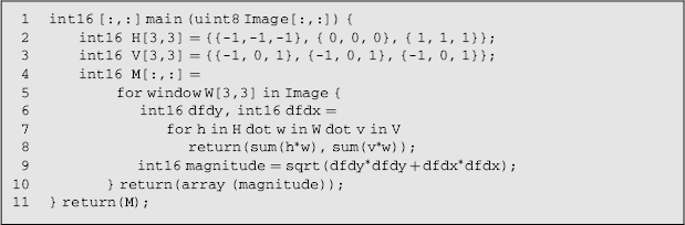
The language can be compiled for serial processing, for simulation and debugging on a conventional processor, or via VHDL to target hardware. The mapping to hardware is facilitated by a library ofconstructs for implementing each of the components.
The lack of a while statement makes other types of operations more difficult. However, the array access mechanisms are efficient for implementing operations that require a scan through the image and provide a higher level representation for those tasks than regular C.
3.2.2.4 A|RT
An early commercial C to HDL compiler was A|RT (for Algorithm to Register Transfer), marketed by Frontier Design. It extends C with fixed-point data types (Johnson and Defossez, 1999). A|RT creates a processor like architecture and uses a VLIW type processor to direct and schedule the operations (Johnson, 2000). The tools allow interactive exploration of different processor architectures during the design. One of the features is the ability to import predefined components (intellectual property cores) into the C programme as function calls. These map to a structural representation in VHDL, allowing optimised code to be directly incorporated into the design. However, as an early generation language, it has not survived (Martin and Smith, 2009).
3.2.2.5 Mitrion-C
Mitrion-C (Mohl, 2006) is a parallel C dialect marketed by Mitrionics specifically targeted towards high performance computing (including image processing). Like SA-C, it is based on the single assignment semantic to simplify extraction of parallelism from the code. Every statement returns a value and performs an assignment, including loops and conditionals. The only effect that a loop or block has on the rest of the programme is through the return value. This enables loops to be executed independently of other parts of the programme. Within a block, all assignments are parallel. The language supports a wide range of types, including variable sized integers and floating-point numbers. Collections of types include lists, vectors and streams. Memory accesses are synchronised through the use of instance tokens, which guarantee the sequential order of accesses.
The basic concept of Mitrion-C is that everything is parallel. Using this concept, a Mitrion virtual processor is created and the language is compiled to that. For an FPGA, the algorithm is accelerated to the maximum extent by unrolling loops (effectively creating multiple parallel processors) until the FPGA is filled. The latest version of their compiler will take the same source code and target an FPGA, GPU or multithreaded CPU exploiting the parallel capabilities of the target platform.
3.2.2.6 Handel-C
One of the difficulties with multiple parallel processes is ensuring reliable communication between them. Simply using shared registers or shared memory only works if the processes are synchronised. One approach is to use the communicating sequential processes (CSP) model described by Hoare (1985). This model requires all communication channels between processes to be unidirectional, point-to-point and blocking. That is the processes at both the sending and receiving end of the channel will wait until the communication successfully takes place before continuing. Using CSP primitives, it is possible to build more complex communication methods, including buffered communication.
The Occam programming language was the first to implement CSP for communication between parallel processes, and as a parallel language this was readily adapted to programming FPGAs (Page and Luk, 1991). Converting the Occam language (and the CSP model) to use a C-like syntax led to Handel-C (Page, 1996).
The Handel-C language was commercialised by Celoxica through the DK Design Suite (an integrated compiler and clock accurate simulator) and quickly established a strong following in the academic community. In 2006, the Handel-C development tools were passed to Agility Design Solutions. In 2009 Agility ceased trading and Mentor Graphics acquired Handel-C and the DK Design Suite.
Handel-C (Mentor, 2010b) extends a subset of C with variable word length integer variables, bit manipulation operations, hardware architectural components (ports, interfaces, RAMs, ROMs), constructs for specifying concurrency through parallel blocks and channel communication between parallel processes. While pointers are allowed, pointer arithmetic is not supported by the language.
The language also provides powerful recursive macros for constructing repetitive complex circuits (for example variable width multiplication and division, or CORDIC calculations). A distinctive feature of Handel-C is that every assignment takes exactly one clock cycle. The resulting strongly timed synchronous design is therefore implicitly at the register transfer level, although using a higher level algorithmic syntax. The compiler internally builds a state machine using a token passing scheme to control the execution and sequencing of commands. The compiler therefore reduces the burden of designing the control logic, as it is implicit in the language constructs. In other respects, though, it is still the responsibility of the developer to identify and exploit parallelism and create pipelines where appropriate. This makes Handel-C an intermediate-level rather than a high-level language. However, even this is sufficient to give significant design productivity over programming in VHDL.
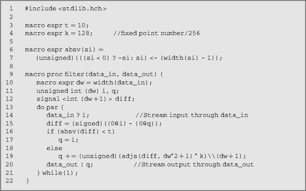
A Handel-C implementation of the circuit in Figure 3.5 is given in Listing 3.3. Lines 3 and 4 define constants for the threshold level and filter gain. The absolute value block is implemented by the macro expression on lines 6 and 7. Since Handel-C is strongly typed, it is necessary to cast the result to unsigned. width(si) is a compile time constant that gives the bit width of si; the expression here is taking the least significant bits, reducing the width by one. The actual filter is represented by the macro procedure on lines 9–22. The arguments of a macro procedure are passed by reference, so any operations on the parameter within the procedure will be directly accessing the caller's arguments. The parameters of macro procedures are untyped, deriving their type from the arguments. This allows macro procedures to be more easily parameterised, whereas the parameters of standard functions must be explicitly typed. Line 10 illustrates one mechanism for such parameterisation by defining dw to be the width of the argument. This is used in the following lines to declare the variables i and q, and the signal diff. Note that signals in Handel-C have a different meaning to those in VHDL. Here a signal corresponds to an unregistered wire. Lines 13–21 contain an infinite loop. The par specifies that all of the statements within the loop are executed in parallel. The data is streamed into the filter through the channel read from data_in on line 14, with the result streamed out through the channel data_out on line 20. Since these are all executing in parallel, if input data is not available or the downstream process is not ready, then the corresponding channel operation will block, stalling the process until the input data is available and the output transferred. In this way, the filter is automatically self-synchronising with the upstream and downstream processes using the CSP model. Lines 15–19 implement the actual filter. Line 15 takes the difference between the input and output. To prevent losing the sign of the result, the widths of the variables are increased by concatenating (@) a 0 on the front. Since diff is a signal, the result is not registered, so this does not take any clock cycles. A signal is used here to reuse the result in multiple places (in lines 16 and 19). Line 19 is effectively executing q += diff ∗ k; however the output of the multiplication in Handel-C is the same size as the inputs, so diff needs to be sign extended (adjs is defined in stdlib.hch) to the desired width. Since k is a constant, it will automatically be made the right width. The result is cast to unsigned and the least significant bits dropped (\) to make it the right width and type for adding to q. While the strong typing is good for detecting errors, the need for casting when the variable widths change can reduce the readability of the code.
Listing 3.3 A Handel-C code fragment to implement the filter shown in Figure 3.5
The Handel-C source can either be compiled to VHDL, or directly to an EDIF net-list. Vendor tools are then used to place and route the design for the target FPGA. These can be integrated within the DK Design Suite as custom build commands, producing the configuration file as the output.
3.2.2.7 Handel-C Derivatives
One of the limitations of Handel-C is that once a program has been developed with the strict timing model, it can be very time consuming to rearrange the algorithm. This makes exploration of the design space more difficult. Haydn-C (Coutinho and Luk, 2003) overcomes this problem by having two distinct formats. One is a strict timing model and structure that closely follows Handel-C, and indeed is compiled to hardware by using Handel-C as an intermediate language. The other format is an untimed dataflow graph that represents the algorithm itself. From this form, the algorithm may be transformed into a range of different structures, enabling exploration of pipelining, loop unrolling, resource allocation and scheduling. A single design can then be used to create a range of implementations guided by a set of annotations in the code. This enables a very flexible exploration of the design space without sacrificing the strict timing model.
Bach-C (Yamada et al., 1999; Kambe et al., 2001) is very similar to Handel-C, and with similar design goals. The main difference is that Bach-C does not have timed semantics. This allows for greater optimisation within each thread. Synchronisation is performed using either synchronous channels (like Handel-C) or asynchronous channels (effectively shared variables or memory).
3.2.3 Native Compilation Techniques
An alternative approach to those described in the previous section is to use standard software source code, and require the compiler to automatically extract parallelism from the design and map the design to hardware. The compilation process may be guided, either with annotations within the source or constraint files that control and optimise the mapping process (Todman et al., 2005). Common optimisations include loop unrolling and automatic pipelining based on an analysis of the algorithm dataflow. By hiding the hardware constraints from the designer, the lower level hardware design is abstracted away, enabling the developer to focus primarily on the algorithm development. Note that the significant differences between the way in which software and hardware are implemented may place some limitations on how the algorithm is coded or restrictions on the language to enable the compiler to identify constructs that may be parallelised. However, most of the work in making the design suitable for FPGA implementation is moved from the designer to the compiler. One of the limitations of this approach is that the compiler is effectively optimising a sequential algorithm, and only the obvious forms of parallelism may be extracted and exploited. The underlying algorithm is still sequential. However, for low level image processing, this approach has been shown to be effective (for example, Streams-C; Gokhale et al., 2000).
3.2.3.1 Transmogrifier C
One of the early efforts at a C to FPGA compiler was Transmogrifier C (Galloway, 1995). It supported a very limited subset of C (no multiplication, division, pointers, arrays or structures). One extension to regular C was the use of pragmas to specify the number of bits used by integers. It provided a simple behavioural method of describing a hardware circuit. The timing semantic was also very simple – there was one clock cycle for each function call and one for each loop iteration. Transmogrifier C was more recently reincarnated as FPGA C on Sourceforge.
3.2.3.2 SUIF-Based Compilers
The SUIF (Stanford University Intermediate Format) compiler system (Wilson et al., 1994; Hall et al., 1996) is a framework designed within Stanford University for collaborative research on parallelising compilers. The framework has been used as the basis for experimental work on compiling from C to HDLs.
The NAPA C compiler (Gokhale and Stone, 1998) works on standard C code and targets the NAPA platform, which consists of a RISC processor coupled with an adaptive logic array. Sections of code can be marked with pragmas to target execution on either the RISC processor or the reconfigurable logic. The compiler pipelines loops targeted for hardware to accelerate their execution.
Streams-C (Gokhale et al., 2000) is an extension of NAPA C to efficiently handle pipelined stream computing. As such, it is able to exploit the parallelism associated with processing streams, with pipeline optimisations performed automatically by the compiler. Directives are added as comment-based annotations that declare processes, streams and signals, and to assign resources to these on the FPGA. A process is a computational block that operates on streamed data. The compiler builds a state machine to control the flow of data through the process pipeline. A library of functions is provided for basic stream manipulations (opening, reading, writing and closing). These link successive processes, including those running on a host serial processor, with inter-process communication based on the CSP model. The same source can be compiled for sequential execution (using threads for each process) or to synthesizable VHDL for FPGA implementation.
One fruitful area of parallelisation is loop unrolling and pipelining. SPC (Weinhardt and Luk, 2001b) takes standard C input and performs loop transformation compiling to a net-list, with the vendor tools used for place and route. ROCCC (Buyukkurt et al., 2006) similarly takes standard C and compiles to VHDL. ROCCC is designed to manage and pipeline two-dimensional arrays and the access patterns required for image processing filters. Smart buffers are used to cache data required in subsequent rows to increase data reuse and reduce the number of memory accesses.
3.2.3.3 Impulse C
Impulse C (Pellerin and Thibault, 2005) is a commercial offering, from Impulse Accelerated Technologies, that follows along the lines of Streams-C. Following the CSP model, the application is divided by the programmer into a set of processes which communicate with one another through streams. This allows the processors with high computation density to be implemented on an FPGA, with the remainder of the application implemented on a serial processor (Pellerin et al., 2005). The development tools (called CoDeveloper) compile modules either to software or to hardware, using a library of streaming functions for software–hardware and hardware–hardware communication. The compiler automatically extracts parallelism, pipelines the design and builds the controlling state machine for each hardware process. However, the developer must still structure the code in a way that maximises the use of hardware resources.
3.2.3.4 Dime-C and DimeTalk
Dime-C (Genest et al., 2007) is a C to VHDL compiler provided by Nallatech. It aims to be ANSI compliant, but does not allow pointers, structures, and some types of loop or switch statements that can be expressed in other ways. The code can be compiled using standard software compilers for testing and debugging the algorithm. When compiled for hardware, pragmas are used to annotate the code to indicate to the compiler sections that contain significant parallelism. The compiler automatically parallelises and pipelines the code when possible.
The compiler can be run on its own or as part of DimeTalk IDE. DimeTalk (Sanderson, 2004) enables the communication between processes both within and between FPGAs to be designed at the conceptual level and it generates the required synthesisable code. Communication is based on a lightweight network architecture for connecting the various modules, with data transferred using a custom, low overhead packet-based protocol.
3.2.3.5 Catapault C
Catapault C (Bollaert, 2008) is a high level synthesis tool provided by Mentor Graphics. It uses standard, untimed C++ code allowing the design to be directly specified at the algorithmic level. It has no specific concurrency constructs – any concurrency is automatically extracted at the compilation and optimisation stage. The only restriction on the language is that everything must be determinable at compile time. This means dynamic memory allocation and recursion cannot be used. The language is extended with a class library that supports variable bit-width integers and fixed-point real numbers, as needed for an efficient hardware design. As standard C++ code, the algorithm can be tested and validated within the standard software environment before synthesising to hardware. Of all the languages reviewed here, Catapault C is the most compliant with C (or C++) in terms of what it is able to synthesise.
The compilation to hardware is controlled by the user by specifying timing and resource constraints. These, combined with characterisations of the target technology, are used to optimise the mapping to hardware through loop unrolling, loop merging, and pipelining. The tools provide several views of the algorithm and its performance, allowing the user to interactively adjust the constraints to efficiently explore the design space without having to rewrite the source code. During synthesis, the communication mechanisms between the different modules are automatically chosen based on the access patterns (stream FIFO, bank-switched memories, round robin memories and other interleaving constructs). The control logic required to schedule and sequence all of the modules is also built automatically. Synthesis then converts the C++ code to RTL in VHDL, Verilog or SystemC, which can then be used to directly generate hardware either for FPGA or ASIC implementation.
3.2.3.6 MATLAB® Based
Many image and signal processing algorithms are first developed and tested in MATLAB®. Therefore, considerable development time would be saved if the MATLAB® code could be synthesised directly to an FPGA. The MATCH project aimed to do exactly this (Banerjee et al., 2000).
Firstly, the MATLAB® code is analysed to determine the operations performed and the data types. This is complicated by the fact that MATLAB® is dynamically typed, with the type changing depending on the results of any assignments. For many operations there are optimised cores (Banerjee et al., 2000), otherwise the code is mapped to sequential code on the FPGA. Matrix operations are expanded out into loops, with complex expressions broken down to simpler expressions. The loops are then pipelined to accelerate the computation. Since most processing in MATLAB® is on large arrays, the input and output arrays are assumed to be in external memory. Speed, therefore, is dominated by memory references (Haldar et al., 2001a; 2001b). The floating-point calculations used by MATLAB® are converted to fixed-point for computation on the FPGA (Nayak et al., 2001; Banerjee et al., 2003). This significantly reduces the hardware and, if the bit width can also be reduced, multiple array elements may be packed into a single memory location, improving the bandwidth. The algorithm is compiled to the target FPGA via VHDL.
Since MATCH was developed, its technology was transferred to a start-up company, AccelChip. In 2006, Xilinx acquired AccelChip and the technology is now available as AccelDSP (Xilinx, 2009a). The design flow still follows the principles outlined above. The MATLAB® code has to follow a particular coding style that assumes streamed input and output data. The floating-point design is converted to fixed-point and verified for fidelity with the original floating-point model. The fixed-point model is then converted to RTL and a test bench created for validation. Acceleration optimisations performed by AccelDSP include partial or full loop unrolling, mapping of variables (arrays) to memory and pipelining. The final design can also be compiled to a block for use with Xilinx System Generator (described in the next section).
Another MATLAB®-based tool is Compaan/Laura (Harriss et al., 2002; Stefanov et al., 2004). This toolset converts a sequential MATLAB® design into a network of independent processes, which is more dataflow orientated. The revised processing model is easier to map to hardware. The data flows from one process to another using blocking FIFOs to ensure correct computation order. Within each process, optimisations such as loop unrolling and skewing are used to improve the implementation.
An alternative to representing an algorithm textually is to use a graphical programming environment and its associated visual language. A visual programming language is one which uses a visual representation to augment what is normally represented purely with text. Textual programming languages are a one-dimensional sequence of commands or statements, which matches the needs of a serial processing environment with a linear program memory architecture. However, programming FPGAs efficiently requires parallel and concurrent programming. A visual language offers multidimensionality (Chang et al., 1999), enabling both spatial and temporal semantic relationships to be expressed more clearly.
At the low level, a schematic diagram is a form of visual language. It enables a network of components to be created with connections between the components indicated by wires. In a textual language, each wire becomes a net name, with the circuit represented by a net-list. Connections are made by listing the net names associated with each port of the component (for example structural VHDL).
Many of the control structures of complex logic systems are based on finite state machines. These can readily be represented graphically using state transition diagrams, such as those shown in Figure 3.4. Therefore, a natural tool for creating and editing finite state machines could be based around the direct editing of the associated state transition diagrams. One example of such a tool is StateCAD, which is part of the Xilinx toolset. While such tools are good for creating finite state machines, this only forms part of the control structure for the complete design.
A range of higher level techniques are reviewed in the following sections.
3.3.1 Behavioural
3.3.1.1 vVHDL
Visual VHDL (vVHDL) (Miller-Karlow and Golin, 1992; Golin et al., 1993) provides a visual representation of VHDL, with different shaped icons and boxes representing concurrent and sequential processes. Otherwise, it provides much the same features as VHDL. Advantages of the graphical representation are that it overcomes the syntax problems associated with VHDL and provides better insight into the function of a design by distinguishing between sequential and concurrent processes (Miller-Karlow and Golin, 1992).
3.3.2 Dataflow
At a higher level of abstraction, both parallelism and pipelining are well represented using a dataflow graph. The parallel nature of FPGAs results in a better fit with dataflow languages, both visual and text based. Indeed, most image and signal processing algorithms are often represented graphically by block diagrams with blocks representing operations on the data, and connections between the blocks indicating the flow of data. Dataflow graphs expose the parallelism of an algorithm, while imposing minimal constraints on the execution order (Buck and Lee, 1993). This allows an appropriate set of hardware processors to be defined for the dataflow. All of the compilers of text-based serial languages (described in the previous section) that automatically extract and exploit the parallelism use some form of dataflow analysis of the algorithm to identify dependencies and parallelism.
This has led to the obvious approach of directly representing image processing algorithms graphically using some form of dataflow language. This can be at two levels: building the algorithm from image processing operations, and at the lower level of dataflow within the individual operations.
3.3.2.1 Khoros Based
Khoros is a software-based image processing environment (Williams and Rasure, 1990), of which Cantata is the dataflow-based graphical programming tool. Within Cantata, each image processing operation is represented by a block, with the blocks wired together according to the dataflow. There have been several research projects using Khoros diagrams as a front-end for targeting FPGA implementations (Hoisko et al., 1996; Levine et al., 1999; Ong et al., 2001).
The basic approach is to have a library of HDL primitives for each Khoros function (Levine et al., 1999). The application can then be compiled by piecing together these primitives based on the dataflow. Since the latency of each primitive is known, synchronising delays can automatically be inserted in parallel paths. Adding a new operation requires providing the underlying code in both C/C++ for the software environment and VHDL for the hardware implementation. These must be functionally equivalent to ensure that the hardware produced will gave the same results as the software algorithm (Ong et al., 2001). This is achieved by using the same fixed-point C/C++ code and compiling it to VHDL to create the library primitives using the A|RT compiler.
3.3.2.2 Simulink Based
Simulink is a graphical dataflow-based programming environment within MATLAB®. It is widely used for DSP-based design and is also applicable for stream-based image processing designs. A number of systems leverage off the environment by providing Simulink block sets for targeting FPGA-based designs. Examples are System Generator from Xilinx (Hwang et al., 2001), DSP builder from Altera (2010c), Synplify DSP from Synplicity (Balakrishnan and Eddington, 2007), and Simulink's own HDL Coder directly from MathWorks (2010). A brief comparison of some of these tools is performed by (Zoss et al., 2011)—there can be quite significant differences in both resources used and processing time between the different tools for the same design. Using the Simulink environment allows application developers without a detailed knowledge and experience of the hardware to produce efficient implementations relatively quickly and effectively. The modelling environment offered by Simulink (and MATLAB®) provides accurate simulation of the design that is considerably faster than that provided by conventional HDLs.
The design flow involves developing the algorithm within MATLAB® and then representing the algorithm graphically within Simulink. At this stage, the specific block sets are used for targeting the design to an FPGA. The design can then be thoroughly tested with bit-level accuracy within the Simulink environment, before being compiled directly to an FPGA. Many of the blocks are parameterisable, allowing the data width and other parameters to be tuned for the design. The block sets from Xilinx and Altera specifically target the advanced DSP features within their respective FPGAs, resulting in an efficient design and use of resources. For example, Altera provides a block set specifically targeted for video and image processing (Altera, 2010f).
The library-based approach hides many of the low level implementation details within the block sets. If all of the blocks required by an application are in the library, then this can be an efficient design approach. However, if a high level block is not available, it is necessary to use quite low level blocks to implement the design, which significantly increases the design complexity and reduces the transparency.
3.3.2.3 Others
LabVIEW is another dataflow-based programming environment. While targeted more for control applications, it can also be used for image processing. LabVIEW provides a set of blocks which have both a software and hardware implementation (National Instruments, 2005). The software implementation is used within the LabVIEW environment for simulating the design, while the hardware implementation is used when targeting an FPGA. When producing an FPGA implementation, the tools effectively use a library-based approach. Again, this has the limitation that only functions available within the library may be used for the design.
Another visual language is the PixelStreams graphical interface to Handel-C (Mentor, 2010c). It uses a library approach to provide a range of image processing operations in a stream based graphical environment. Each operation is written in Handel-C, so is readily extensible. The operations are connected using a consistent stream based interface which consists of a number of control flags and a range of data variables: pixel values, coordinates, and synchronisation pulses. The common interface makes the operations plug and play, with the resulting system compiled and implemented by the underlying Handel-C compiler.
3.3.3 Hybrid
While dataflow languages provide a good match for a parallel hardware implementation, unless the control can be embedded with the data, the control tends to be hidden. Directly expressing complex control within a dataflow language can be clumsy. Therefore, a hybrid approach can give improvement, where a dataflow representation is used for streaming data and a finite state machine can be used for designing the more complex control.
3.3.3.1 VERTIPH
The Visual Environment for Real Time Image Processing in Hardware (VERTIPH) (Johnston et al., 2004;; Johnston, 2009) is the approach that Massey University is investigating to address this issue. The representation of a design is divided into three main views. At the top, the architecture view provides a high level dataflow representation of the image processing algorithm in a manner similar to that used by Khoros or PixelStreams. The computational view is a timed dataflow representation of the computations required to implement each operation; this is at a similar level to that of the inner blocks within a Simulink representation. Finally, the scheduling view uses augmented state transition diagrams for providing the complex control, for scheduling each of the computational blocks and for managing shared resources.
The architecture view comprises a hierarchical block and wire representation of the algorithm (Johnston, 2009). The top level gives an overall view of the complete algorithm. Since the top view must be constructed first, VERTIPH enforces a top-down design. If necessary, each architectural block can be decomposed into a networked collection of either other architectural blocks or computational blocks as illustrated in Figure 3.6. The hierarchical nature of architectural blocks enables resources to be encapsulated with their controlling processes (for example a bank-switched frame buffer). Although such encapsulation is not enforced by the language, it follows good design principles for hiding complexity from where it is not needed, and helps to improve the reusability and maintainability of components. The wires between blocks can carry both data and control signals. The connections also use a hierarchical data structure (similar to structs in C) to hide unnecessary details from the diagram. An example architectural view is shown in Figure 3.7. Note that the control flow (shown in grey) flows in a different direction to the dataflow in many cases. Image processing specialists who never develop their own operations can use the architectural view to assemble predefined library modules into their design.
Figure 3.6 Hierarchical structure of a VERTIPH design. (Johnston, 2009; Reproduced by permission of C. Johnston.)
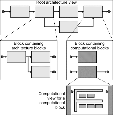
Figure 3.7 VERTIPH architectural view for lens distortion correction. (Johnston et al., 2004; Reproduced by permission of C. Johnston.)
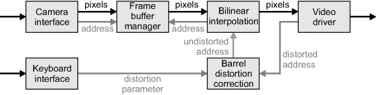
The computational view specifies the arithmetic and logic operations required to implement each block within the design. To encourage functional decomposition, it is also hierarchical, allowing computational blocks to be used in place of operation blocks. Like the architectural view, the computational view follows a dataflow style, but also introduces control constructs (loops and conditional executions) using a graphical representation modified from Nassi–Shneiderman diagrams (Nassi and Shneiderman, 1973). The control structures enclose the operations that they control, making the structure more evident. The syntax also introduces a strict timing semantic, with each operation assigned to a particular clock cycle, with the horizontal axis used to indicate time whereas the vertical axis indicates concurrency. The visual structure more clearly conveys the intention of the code, with a clear distinction between sequential, parallel and pipelined operations. The VERTIPH computational view for Figure 3.5 is illustrated in Figure 3.8.
Figure 3.8 VERTIPH computational view for the filter shown in Figure 3.5.
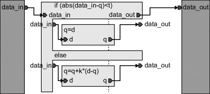
VERTIPH is unique in its representation of pipelines. All other languages consider pipelines as a special case of concurrent operations, reflecting the fact that each stage of the pipeline operates concurrently. However, from a dataflow perspective a pipeline is really a sequential construct. The fact that other data is also being processed in the other stages is immaterial to the dataflow (Johnston et al., 2010). Separating the sequential semantic aspects from the concurrent syntactic aspects significantly improves the transparency of the design. The representation used clearly shows the timing, throughput and latency of the design. Exploration of the design at this level is facilitated by giving the designer to direct control over the pipeline phasing. Having an explicit representation of the pipeline can also aid with pipeline control, enabling priming, flushing and stalling circuitry to be instantiated automatically in many cases (Johnston et al., 2010).
The third view within VERTIPH is the scheduling view. The primary purpose of this view is to control when each of the computational blocks is executed, and to manage resource contentions. For simple systems, the resource and scheduling view is not necessary; all of the controls may be specified by using conditional structures directly within the individual computational views. However, as the system grows in complexity, this can become unwieldy, especially as one change may require consequent changes in other computational blocks. Centralising the high level control in a single view makes the process more manageable. The scheduling view has two parts (Johnston et al., 2008). The first part consists of one or more state transition diagrams. These may be controlled by either external events or internal counters. In each state, one or more processes (computational blocks) may be scheduled to execute. The second part of the view indicates which processes are associated with each state. When multiple processes are associated with a state, these may be scheduled sequentially, concurrently, or as a pipeline. When multiple processes share a common resource, potential conflicts may arise. Many resource conflicts are simplified by encapsulating the resource and its conflict resolution processes within a single architectural block.
At the time of writing, the VERTIPH language does not include a simulator or compiler, but the language is described here to give a flavour of the approaches that can be taken for implementing image processing systems.
Four quite different approaches to programming an FPGA have been presented in this chapter. Hardware description languages (VHDL and Verilog) are good at describing hardware, and are inherently concurrent. Their main limitation is that they require programming at the structural level or register transfer level, which is quite different from the algorithmic approach to representing image processing algorithms. Consequently, the algorithm is usually developed within a software environment, leaving the laborious and error-prone task of translating it from the software into the HDL.
Conventional software languages, such as C and MATLAB®, are much better for representing algorithms, so if the translation step from software to HDL can be avoided, significant gains in productivity can be achieved. Two approaches are taken for using these languages to programme FPGAs. One is to extend the language to enable it to describe hardware, by adding concurrent constructs. The result is a software-based hardware description language – it retains the algorithmic structure, but is able to describe concurrent hardware. The conversion from software to hardware is then one of refinement, rather than rewriting the algorithm from scratch. The other approach is to leave the language unchanged, but to enhance the compiler to automatically identify and extract any parallelism from within the algorithm. The limitation of this approach is than many algorithms are represented serially, and are optimised for implementation on serial processors. While there may be parallelism that can be exploited, unless the underlying algorithm is essentially parallel it is not going to give the most efficient solution. The danger here is that the wrong algorithm is being parallelised and parallelising serial algorithms is not trivial.
The fourth approach is to use some form of visual language to represent the operation of the hardware. For many image processing algorithms, a dataflow representation exposes the natural parallelism inherent within the algorithm. One limitation of visual languages is that the representation is significantly more expansive (requires more screen real-estate), making it harder to maintain an overall view of the whole algorithm. In exposing the flow of data through the system, the control flow can also become obscured.
None of the current offerings is perfect (Martin and Smith, 2009). Which is best? The answer depends on the goals. A solution hand crafted in an HDL using a structural coding style will generally give the smallest and fastest design, although the development process is very time consuming. Using a C-based language gives higher productivity, but this often comes at the expense of a larger and slower design. The compiler orientated approaches will usually enable a faster exploration of different architectures, as these can often be set up as compiler constraints. Library-based approaches (whether using a textual or visual language) can be very efficient if all of the required functions are available within the library. The design then becomes one of piecing together library components, which usually have implementations that have been optimised for a particular family of FPGA.
In the Massey University laboratory, a combination of VHDL and Handel-C is used. VHDL is used primarily for developing interfaces to external components where precise control is required. All of the algorithmic design is in Handel-C, which is an intermediate level C-based hardware description language. This gives significant productivity gains over VHDL through its higher level algorithmic representation, but also enables control at the lower levels where necessary.
It is important to keep in mind that FPGA-based development is hardware design. Design for hardware and for software requires different skills. Even if a C-based language is used to represent the design, it is important to keep in mind the architecture that is being built or is implied by the algorithm. Not all software algorithms map well to hardware. For example, recursion is not available unless hardware is explicitly built for saving the context and recalling it again later (Skliarova and Sklyarov, 2009). Under real-time constraints, there is limited access to memory. These and many other aspects of hardware design usually require that the algorithm be transformed rather than simply mapped to hardware. Again, this requires a hardware orientated mindset.
Image processing algorithm development, however, is usually considered software design. Therefore, the development of efficient FPGA-based image processing systems requires a mix of both hardware and software engineering skills. The differences between these is explored in more detail in the next chapter.