
Chapter 13
Testing, Tuning and Debugging
In any application, it is the fortunate developer who can get the system to function as desired on its first attempt. Inevitably, there are errors in either the design or implementation that require the algorithm to be tuned or debugged.
There are four main causes for an algorithm not behaving in the intended manner that are addressed briefly in this chapter. These are:
- Design errors This encompasses a range of issues including faulty logic and the algorithm being unsuitable or not sufficiently robust for the task. A rigorous design process should eliminate such errors before reaching the FPGA implementation stage. However, many development applications follow a less formal design-as-you-go process, where such design errors can be expected!
- Implementation errors Syntax errors such as spelling mistakes, incorrect operations and misplaced parentheses will usually (but not always) fail to compile. More subtle errors result from the implementation not matching the design. These include errors in the mapping of operations onto the FPGA, such as not correctly taking into account the latency. Particular problems can relate to conflicts between subsystems working in parallel.
- Tuning errors In this class, the algorithm is basically correct, but the parameters are such that it does not behave in the intended manner. Tuning involves finding the set of parameters that gives the best performance.
- Timing errors These result from the algorithm being logically correct, but being clocked too fast for the propagation delays of the logic. Systems run at the limit of their performance may fail intermittently as setup and hold times of registers are violated.
A range of techniques were discussed from a design perspective in Section 5. These will not be examined again in this chapter in any detail, although they will be reviewed as appropriate under each of the categories above.
As outlined in Chapter 4, the design of an image processing algorithm for a particular task is a heuristic process. It requires considerable experimentation to develop the sequence of image processing operations to achieve the desired result. A software-based image processing system provides the level of user interaction required to try different operations and examine the results.
The main issue with algorithm design is how to go about testing a complex algorithm. In all but trivial cases, it is impossible to test an algorithm exhaustively. No algorithm is perfect; all will have flaws or limitations. The primary role of testing is, therefore, to determine the useable limits of the algorithm and determine its robustness.
The conventional approach to testing digital logic is to develop a test bench which exercises all of the components of the design and validates that the design is correct. With image and video processing, however, this approach is impractical because of the large input space. A single low resolution, 256 × 256 greyscale (8 bit) image has a total of 524 288 bits. This gives 2524288 different images. While only a small fraction of these are ‘useful’ in any sense of the word, and, of those, even fewer images may be relevant to a particular task, the number of images likely to be encountered in any application is still impractically large to test exhaustively. By today's standards, a 256 × 256 image is small. Larger images and image sequences (video) contain even more raw data, compounding the problem.
Testing an image processing algorithm therefore only considers a selection of sample images. In addition to a range of typical cases, it is important to use images which test the boundaries of correct operation. When using image processing to detect defects, it is particularly useful to have a large proportion of the test images near the classification boundaries. If necessary, the available images may be modified artificially to simulate the effects of changes in lighting, to adjust the contrast or modify the noise characteristics.
Test patterns and noise sources may be used to create test images or modify existing sample images to simulate effects which may occur rarely. For example, uneven lighting may be simulated by adding an intensity wedge to an image. The noise sensitivity of an algorithm may be tested by adding increasing levels of random noise to an image to determine the level at which the algorithm becomes too unreliable to be usable.
While some testing may be performed in software, in some applications the system must be tested on-line to achieve a suitably wide range of inputs. However, before getting this far, the developer should be fairly certain that the algorithm is not going to change significantly. Most of the adjustments should be parameter tuning rather than wholesale algorithm changes (unless of course the testing determines that the algorithm is not sufficiently robust or is otherwise deficient in some way).
13.1.1 Random Noise Sources
When adding noise to an image, it is necessary to have a source of random numbers. Two main types of random number generators may be implemented on an FPGA: true random number generators and pseudorandom number generators. Two techniques for generating true random numbers (Danger et al., 2007; Tsoi et al., 2007) are to rely on metastability (deliberately violating setup and hold times) so that the output is effectively random, and to sample a high speed clock signal with a slow but unstable clock. The jitter of the latter makes the sampled clock random. Two limitations of true random number generators are that the bit generation frequency is relatively low and that the sequence cannot be regenerated without storing it.
Pseudorandom number generators produce deterministic sequences which pass many of the tests of true random numbers. These work by maintaining a Boolean state vector, x, with the next state determined as some function of the current state. The output vector, y, is also some function of the current state. The most common form of hardware-based random sequence generator is a linear recurrence generator, where the function is given by the matrix:
with all of the operations performed using modulo-2 arithmetic. With this multiplication becomes an AND gate and addition becomes exclusive OR. Since matrices A and B are constant, this is equivalent to each state variable being the exclusive OR of some combination of the state variables, as shown on the left in Figure 13.1. With appropriate selection of A, the length of the sequence is ![]() , where N is the number of bits in the state vector. Such sequences are called maximal length sequences. The −1 comes from the fact that a state vector of zero will always produce a zero result using such a linear combination. Therefore, it is essential to initialise the state vector to be other than all zeros, otherwise a random sequence will not be generated. An implementation of Equation 13.1 optimised for FPGA implementation is described by Thomas and Luk (2005). The multiplication of each row of A was implemented using a single 4-LUT on the FPGA to combine up to four state variable bits to produce each output bit, giving a resource efficient implementation.
, where N is the number of bits in the state vector. Such sequences are called maximal length sequences. The −1 comes from the fact that a state vector of zero will always produce a zero result using such a linear combination. Therefore, it is essential to initialise the state vector to be other than all zeros, otherwise a random sequence will not be generated. An implementation of Equation 13.1 optimised for FPGA implementation is described by Thomas and Luk (2005). The multiplication of each row of A was implemented using a single 4-LUT on the FPGA to combine up to four state variable bits to produce each output bit, giving a resource efficient implementation.
Figure 13.1 Linear recurrence random number generators. Left: general case with ![]() ; right: linear feedback shift register with two output bits.
; right: linear feedback shift register with two output bits.
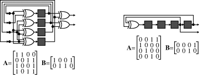
One class of linear recurrence generator is the linear feedback shift register (LFSR), which uses the feedback for only one state variable, with the others obtained by shifting the bits along. Although multiple bits may be obtained from an LFSR, as shown in the right in Figure 13.1, the problem is that the bits are related by a simple shift and are not independent. This problem may be addressed in a number of ways.
- Use several such generators (with different feedback combinations), each producing one bit output. If the generators have coprime maximal lengths, then the length of the output sequence will be the product of the lengths.
- Combine multiple bits together (using a B matrix) to improve the independence. The bits combined should be random rather than in a sequence.
- Taking k bits output every k clock cycles. This ensures that an independent set of bits is provided each time. A variation on this is to shift the data by k positions each clock cycle. This effectively uses
 rather than A as the state transition matrix. An example is shown in Figure 13.2 for
  .
. - A combination of the above can be used to improve the statistical properties of the output.
Figure 13.2 Producing multiple output bits by shifting several positions each clock cycle. Top: original 10-stage LFSR shifted by one bit; bottom left: shifted by two bits; bottom right: rearranged to show coupled LFSR implementation.
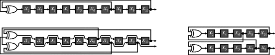
Looking in more detail at Figure 13.2, one 10-stage maximal length LFSR is represented by the feedback:
(13.2) ![]()
which on the next clock cycle is clocked into ![]() . When shifting everything by two places it is necessary to have two sets of feedback, representing successive shifts:
. When shifting everything by two places it is necessary to have two sets of feedback, representing successive shifts:
(13.3) ![]()
This may be readily extended to shifting any number of places. When shifting multiple places, the state bits fall into distinct groups, each of which is a standard shift register but with cross-coupled feedback, as demonstrated on the bottom right in Figure 13.2. As long as ![]() is not a factor of
is not a factor of ![]() , then the length before the sequence repeats is unchanged. Obviously for image processing
, then the length before the sequence repeats is unchanged. Obviously for image processing ![]() is far too small. For practical use, the sequence length should be significantly longer than the number of pixels in the image. (For
is far too small. For practical use, the sequence length should be significantly longer than the number of pixels in the image. (For ![]() the following all give maximal length sequences:
the following all give maximal length sequences: ![]() ,
, ![]() ,
, ![]() ,
, ![]() ,
, ![]() ,
, ![]() ,
, ![]() , and
, and ![]() . For
. For ![]() , there are no two feedback maximal length combinations, but there are many four feedback combinations including
, there are no two feedback maximal length combinations, but there are many four feedback combinations including ![]() ,
, ![]() ,
, ![]() , and
, and ![]() .)
.)
The numbers produced by most pseudorandom number generators have a uniform distribution. To produce numbers with a different distribution (for example Gaussian) then a lookup table containing the inverse cumulative distribution can be used to transform the input to the corresponding output. This follows the same procedure as histogram shaping illustrated in Figure 7.14. If necessary, to maintain precision, an interpolated lookup table (Section 2) can be used to map wider data words.
For a Gaussian distributed sequence of random numbers, with programmable mean and variance, an alternative is to use a single lookup table to generate a normal distribution (![]() ,
, ![]() ), then scale this by the standard deviation and offset by the mean:
), then scale this by the standard deviation and offset by the mean:
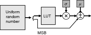
Since the transformation from uniform to normal distribution is symmetric, the resolution can be doubled for the same size lookup table, with the MSB used to select addition or subtraction, as shown in Figure 13.3.
Figure 13.3 Gaussian random number generator.
If multiple correlated numbers need to be generated, then Equation 13.4 may be adapted by scaling vectors:
where
(13.6) ![]()
and ![]() is the covariance matrix. For a given covariance matrix,
is the covariance matrix. For a given covariance matrix, ![]() is not unique and may be derived by many techniques. To generate
is not unique and may be derived by many techniques. To generate ![]() correlated output numbers, the multiplication by
correlated output numbers, the multiplication by ![]() requires
requires ![]() individual multiplications. Alternatively,
individual multiplications. Alternatively, ![]() lookup tables can be used to produce the scaled Gaussians (Thomas and Luk, 2009), which are then added with the mean vectors. That is, Equation 13.5 is expanded to:
lookup tables can be used to produce the scaled Gaussians (Thomas and Luk, 2009), which are then added with the mean vectors. That is, Equation 13.5 is expanded to:
(13.7) ![]()
where each term within the summation is generated by a separate lookup table.
As well as noise images, other test patterns can also be generated and used for testing algorithms or for modifying images to test a wider range of circumstances.
The mapping from the initial software representation to a hardware implementation can introduce errors within the algorithm. Rather than test the complete application level algorithm as a unit, it is far easier to test each image processing operation and verify that it is behaving as designed.
Verifying each operation level algorithm is simpler than verifying the complete application level algorithm in one step. This is because it is easier to test each operation more thoroughly when directly providing input to that operation. When testing as a sequence, some states or combinations may be difficult or impossible to test given the preceding operations. If each operation behaves the same as its software counterpart, then the complete algorithm should also operate correctly. Testing consists of providing one or more images which exercise each aspect of the algorithm and validate that the correct output is being produced.
While the algorithm can be validated through simulation, this is often quite slow for complex designs. This is another reason for testing each operation individually before combining them to create the application level algorithm. Conventional simulators operate from a hardware perspective and usually provide the waveforms of selected signals. Although this can be useful for validating timing and synchronisation, it is less useful for algorithm debugging, which is best achieved with a software style debugger.
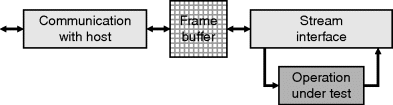
A structure for testing the operation of an algorithm on an FPGA is given in Figure 13.4. It consists of two main sections. The communication with the host is used to load test images into the frame buffer and retrieve the output images. If resources on the FPGA are tight, this may be implemented as a separate configuration from the actual test operation. The second section is the stream interface, which is used to interface between the test image(s) in the frame buffer and the operation under test. It is responsible for reading the data from the frame buffer and converting it into a pixel stream as required for testing the operation. It simulates image capture and any necessary processing steps prior to the operation under test. It also takes the output stream and stores the results back into the frame buffer (or another frame buffer depending on resources available and memory bandwidth). The output is then retrieved from the frame buffer by the host and compared with the expected output (produced for example by running the software version of the algorithm on the host). Any differences indicate potential errors in the implementation. The lack of differences is only significant if the input image exercises all parts of the algorithm.
Figure 13.4 Configuration for testing each image processing operation.
Testing the algorithm with a low clock frequency will also remove potential timing issues from the test. This enables the test for functionality to be separated from potential clock rate and propagation delay issues.
While such a system can provide a pass or fail indication, it is of limited value in debugging the algorithm. Several methods of debugging were outlined in Section 2. To review, these are:
- Route key signals to unused I/O ports. This makes them observable from outside the FPGA, enabling monitoring by an external oscilloscope or logic analyser.
- Embedding a logic analyser within the design. Both Xilinx (ChipScope; Xilinx, 2008a) and Altera (SignalTap; Altera, 2008e) provide embedded logic analysers with their development toolsets. These can monitor selected signals, recording their history in block memory enabling later readout and analysis with associated tools.
- Stop the system and read back the configuration to analyse the logic state at the time the system was stopped. When using a hosted system, one of the main limitations is the latency in transferring data between the FPGA and the host system.
- This can be augmented with a small amount of additional logic to enable hardware single-stepping by gating the clock (Tombs et al., 2004). Using logic to detect key events can provide the system with hardware breakpoints. Iskander et al. (2010) extended this idea by controlling the process with an on-chip microprocessor that uses a software style debugging interface for debugging the hardware in place. They used the internal ICAP port of Xilinx FPGAs to read back selected variables to provide true hardware debugging.
Of course, any combination of these techniques can be used, combined with simulation of the operation within the development environment.
13.2.1 Common Implementation Bugs
Experience has shown that there are a number of common bugs which occur during the implementation phase. This list is not exhaustive, but serves as a guide for investigating possible causes of malfunctions.
Hardware allows the bit widths of variables to be adjusted to minimise the hardware resources required. A common cause of errors is to underestimate the number of bits required by an application. There are two main consequences of having too few bits: overflow and underflow. Overflow occurs when the numbers exceed the available range. With most arithmetic operations, the effect of overflow is for the numbers to wrap around, becoming completely meaningless. During debugging and development, additional logic can be added to detect overflow. This requires adding an additional bit, ![]() , to a register. Overflow is then detected as:
, to a register. Overflow is then detected as:
(13.8) ![]()
After thoroughly testing the algorithm, the extra test hardware can be removed in the final implementation. Overflow can be corrected by adding extra bits, or by rescaling the numbers.
At the other extreme, underflow occurs when too many bits have been truncated from the least significant end. The effect of underflow is a loss of precision. Underflow occurs primarily when working with fixed-point designs, or when using multiplication and division. It also shows when reducing the size of lookup tables to reduce resources. Underflow is harder to test for with hardware. During the development stages (in software) a range of designs can be compared with different numbers of least significant bits to check that the errors that arise through truncation are acceptable. Underflow can also be affected by the order in which arithmetic operations are performed, especially when using a floating-point representation. Some applications may require one or more additional least significant guard bits during intermediate steps to reduce the loss of precision.
Both overflow and underflow reflect incomplete or inadequate exploration during the design stages of the project.
Closely related to overflow is the wraparound of array indices (unless this is intentional). A similar problem occurs in C programming, especially when using pointers and pointer arithmetic. Apart from the fact that such errors are errors whether in hardware or software, in a hardware system the effects are usually less severe. In software, with its monolithic memory structure, extending past the end of an array will go into following memory and can corrupt completely unrelated variables. In hardware, the effects are usually local. If the array is not a power of two, then there may be no effect if the hardware past the end of the array does not exist. Otherwise extending past the end of an array will usually wrap back to the start. The localisation of such errors can make them easier to track and locate in hardware than software. If necessary, additional hardware may be built which detects array bounds errors (and overflow of the index variable).
Another error relating to data word length is misalignment of data words when performing fixed-point operations. Most hardware description languages have integers as a native type (even if implemented as a bit array), but do not have direct support for fixed-point numbers. It is over to the user to remember the implicit location of the binary point and align the operands appropriately when performing arithmetic operations. The manual processing required can make alignment tedious to check and misalignment bugs difficult to locate. Errors are easily introduced when changing the size or precision of a variable and not updating all instances of its use. This may be overcome to some extent by using appropriate parameterised macros to maintain the representation and manage the alignment. The design of an appropriate test bench should detect the presence of any data misalignment errors.
The parallel nature of FPGA-based designs can result in additional bugs not commonly encountered in software-based systems. One of the most common of these is to write to a register (or access to any other shared resource) simultaneously from multiple parallel threads. The synthesiser will normally build a multiplexer to select the inputs, and if multiple inputs are selected the result may be a combination of them. Hardware can be added to a design to detect when multiple inputs are selected simultaneously when the multiplexer has been added explicitly to the design (for example using a structural programming style). However, when using a behavioural programming style, such multiplexers are added implicitly and it will be difficult, if not impossible, to detect the selection of multiple inputs.
Multiplexing errors result from bugs within the control logic. These can be caused by the parallel streams not being synchronised properly or by failure to build appropriate arbitration logic. Explicitly building in arbitration (Section 2) can provide error signals when a parallel thread is blocked from using a resource.
Pipelines with multiple parallel data paths can also suffer from synchronisation problems. Temporal misalignment can occur not only within an operation level algorithm but also within the higher application level algorithm, making such errors hard to detect. Most hardware description languages treat pipelining as simply another case of parallelism and rely on the developer to implement the correct pipeline control (in particular priming and flushing). The higher level, C-based languages, where the compiler automatically detects parallelism from the dataflow and implements pipelining, are better in this regard.
Synchronisation between clock domains is another complex issue prone to error. If throughput is not critical, a channel may be used, but for higher throughput (for example sending pixel data) use of a FIFO is essential. The resulting non-uniform data rate on the receiving side of the transfer can cause a wide range of synchronisation and control issues.
To summarise this section, if the software version of the algorithm behaves correctly then there are two primary sources of error within the corresponding hardware implementation. The first relates to customisation of data word widths and the second relates to the use of parallelism with consequent synchronisation and conflict issues.
Most algorithms require some tuning of parameter values such as threshold levels to optimise their performance. The requirements for tuning an algorithm were covered in some detail in Section 1.The basic structure for algorithm tuning is shown in Figure 13.5.
Figure 13.5 Generic structure for algorithm tuning.
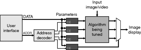
Firstly, a mechanism must be provided for dynamically changing the algorithm parameters. Recompiling the application each time a parameter is changed is not particularly practical and methods of modifying the parameter through directly manipulating the configuration file are not particularly transparent or portable. Altera provides a mechanism where selected register and memory contents may be changed or edited manually within the system (Altera, 2008e). A standard approach used by many ASICs is to provide a set of addressable control and status registers. These provide a flexible mechanism for directly setting algorithm parameters and can also be used for monitoring the algorithm status. These registers are usually accessed either via a low speed serial interface or a microprocessor style interface with parallel address and control busses.
The second key requirement is some form of user interface for manipulating the parameter and visualising the results of the changes. On a hosted system, the host computer can readily provide such a user interface. If the two are connected via a high speed interface such as PCI express, then the host may also display resultant image data as well. Otherwise it may be beneficial to provide some form of image display directly from the FPGA. On a stand-alone system, such a user interface may be implemented through an embedded processor. Otherwise the complete interface will need to be implemented directly in hardware (Buhler, 2007).
Timing is a critical issue in any high performance design. Timing closure is the step of taking a functionally correct design and getting a working implementation that meets the desired operating speed and timing constraints.
Timing closure has become more difficult with each successive technology generation. Older FPGAs were relatively small, so both the complexity and the speed of a design were limited. Modern FPGAs are significantly larger and capable of being clocked at a much higher speed. Consequently, the scale of applications being implemented on FPGAs has grown, not only in complexity but also in target operating speed. Consider for example image processing. Clock speeds from video cameras are relatively low and many early implementations of image processing on FPGA focussed on simple image processing operations and small local filters. However, the resolution of digital cameras has increased significantly in recent years. To maintain video frame rates, this has required a corresponding increase in pixel clock frequency by almost an order of magnitude. The complexity of image processing algorithms implemented on FPGAs has also grown. As a result, bigger and faster designs are being implemented on bigger and faster chips.
There are two aspects or components to timing closure: one is ensuring that the design on the FPGA can be clocked at the desired rate and the other is meeting the timing constraints of devices external to the FPGA. As device scales have shrunk, an increasing proportion of the propagation delay between registers on the FPGA is coming from the routing (Altera, 2009b). With high clock speeds and large FPGAs, the propagation delay from one side of the chip to the other can exceed the clock period. Therefore, it is essential to keep related logic together to minimise propagation delay. When interfacing to peripherals external to the FPGA, it is important to have the logic placed relatively close to the associated I/O pins. I/O drivers also introduce a significant propagation delay, as do the relatively long tracks on the printed circuit board (PCB) between the FPGA and peripheral. For high speed devices, such as DDR memory, even the skew between parallel signal lines becomes significant (this is why many high speed peripherals are going to even higher speed, serial connections with the clock embedded with the signal). Fortunately, many of these problems, at least within the FPGA, are managed by the FPGA vendor's tools, which can optimise the placement and routing of designs based on timing constraints specified by the developer.
The tools also provide a timing report which details the timing characteristics of the design. Such a report is based on a static timing analysis – after the design has been placed and routed on the FPGA, the propagation delay through each component and routing wire can be modelled and analysed against the timing constraints. The report will identify any timing violations, the associated critical paths and determine the maximum operating frequency of a design. However, there are three limitations of such an analysis.
The timing analysis is usually based on the worst case conditions. This usually corresponds with the performance of the slowest device, operating at the maximum temperature and minimum power supply voltage. Consequently, passing under these conditions will guarantee that the propagation delay will be shorter than the clock period, taking into account register setup times and any clock skew. With modern high speed devices it is also necessary to repeat the analysis under best case conditions (Simpson, 2010) (fastest device, operating at the minimum temperature and maximum power supply voltage) to ensure that register hold times are also met, given the worst case clock uncertainty or skew.
The second limitation is that the timing analysis is only as good as the constraints provided by the user. If a path has no timing constraint, it will not be analysed and any timing violation will not be reported. This can cause a design to fail. Timing constraints are used not only for timing analysis, but are also used by the place and route engine to determine where to focus its effort and optimisations during fitting. Changing any of the source files will change the placement seed, resulting in a different initial placement. Changing the timing constraints in general will change the order in which paths are optimised, resulting in a different layout and different timing. It is important to specify realistic timing constraints. If too tight, then the compile times can increase significantly as the place and route tools try to satisfy the constraints. Timing constraints are also essential when interfacing to external devices. In setting such constraints, it is also important to take into account the propagation delay of the PCB tracks and clock skew.
The third limitation of static timing analysis is that it can only identify errors within a synchronous design. With multiple clock domains, the clocks in each domain are usually relatively asynchronous. Even when operating at the same frequency, unless one clock is locked to the other, the phase relationship between them is unknown and cannot be relied on when directly transferring data from one domain to the other. When the frequencies are different, the relative phase is always changing, so specifying timing constraints between domains is virtually impossible. Therefore, it is essential that appropriate synchronisation logic be built whenever signals traverse clock domains. Suitable synchronisation logic was described in Section 5.1.3.
Designs that pass timing analysis but have timing errors typically do so for two reasons. The first is that an appropriate time constraint was not set for the path. With multiphase designs, the setting of suitable constraints is complicated by the fact that the clock might not be enabled on every clock cycle. In such cases it may be perfectly legitimate for the propagation delay to take up to two or three clock cycles before the register is enabled. Specifying such paths as multicycle paths in the constraints file aligns the constraints with reality. (It also avoids unnecessary effort on the part of the place and route tools trying to reduce the propagation delay to smaller than it needs to be.) The second problem is metastability resulting from asynchronous signals. This is caused by inadequate synchronisation of signals between clock domains. Problems caused by asynchronous signals can be much harder to detect and debug because they are often intermittent.
If a design is failing timing constraints, consider the following checklist:
- Use realistic timing constraints. Specifying a higher clock speed will result in a faster design up to a certain point. This comes at the cost of increased optimisation effort giving larger compile times. Setting the desired clock frequency beyond that which can realistically be achieved will drastically increase the compile times, without achieving timing closure. As the device use increases, the achievable clock speeds tend to reduce because there is less freedom available in optimising the critical paths.
- Identify multicycle or false paths. These can give false failure warnings. They also cause the compiler to spend unnecessary effort trying to make these paths conform to the timing constraint.
- Use low level pipelining. Deep logic has a long propagation delay and may need to be pipelined to meet performance targets. Also consider pipelining the control path, as this can also add to the propagation delay, especially with a series of nested conditional statements. Assigning to a register from multiple sources will build a multiplexer on the register input increasing the number of layers of logic. Propagation delay can be decreased if separate registers are used for each instance if the design allows.
- Reduce high fanout. A signal that is used in a large number of places may be subjected to excessive delay, especially if the signal is distributed over a wide area of the chip. Duplicating the driving registers in different parts of the design can reduce the fanout and increase the locality of the design.
- Register I/O signals. When working with high speed signals, both inputs and outputs should be registered within the I/O blocks. Related signals should use the same I/O banks where possible to reduce differences in propagation delay. Some FPGAs have programmable delays in the I/O blocks to balance small differences in delay.
- Use modular design with incremental compilation. If the compile times are excessively long, split the design into modules and use incremental compilation. For this, each module is compiled separately and the layout within modules is not changed when bringing the modules together under the top layer. The reduced compilation times come at the expense of poorer performance for signals spanning between modules (Simpson, 2010). Where possible, module inputs and outputs should also be registered so that the only delay between them is the inter-module routing. Incremental compilation can also result in reduced flexibility in optimising the placement and routing of the top layer of the design. Such techniques can therefore become less effective as the design approaches the capacity of the FPGA.
To conclude, timing and timing closure are not just considerations at the end of the implementation, but need to be considered at all aspects of a design, from the initial specification all the way through design and implementation.