
Chapter 2
Field Programmable Gate Arrays
In this chapter, the basic architectural features of FPGAs are examined. While a detailed understanding of the internal architecture of an FPGA is not essential to programme them (the vendor-specific place and route tools manage most of these details), a basic knowledge of the internal structure and how a design maps onto that architecture can be used to develop a more efficient implementation.
The basic idea behind programmable hardware is to have a generic circuit where the functionality can be programmed for a particular application. Conventional computers are based on this idea, where the ALU can perform one of several operations based on a set of control signals. The limitation of an ALU is that it can only perform one operation at a time. Therefore, a particular application must be broken into the sequence of control signals for controlling the function of the ALU, along with the logic required to provide the appropriate data to the inputs of the ALU. The sequence of controls is provided by a sequence of programme instructions stored in the memory.
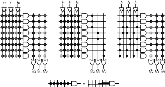
Programmable logic, on the other hand, represents the functionality as a circuit, where the particular circuit can be programmed to meet the requirements of an application. The key distinction is that the functionality is implemented as a parallel system, rather than sequential. Any logic function may be implemented using a two-level minterm (OR of AND) representation. Therefore, it made sense that early programmable logic devices consisted of a two-level programmable array architecture, such as that shown on the left in Figure 2.1. Each of the inputs (and its inverse) can potentially be connected to the input of each of a set of AND gates. Each circle represents a programmable connection between the corresponding vertical and horizontal line, as shown in the bottom of Figure 2.1. A similar arrangement is used to connect the output of each of the AND gates to the inputs of the OR gates. In practice, both input and output sections use the same circuit since, from De Morgan's theorem, the OR of ANDs can be implemented as a NAND of NANDs. Sequential logic, such as counters and finite state machines can be implemented with the addition of latches or flip-flops on the output, and appropriate feedback from the output back to the input.
Figure 2.1 Types of programmable logic array. Left: both the input AND and output OR sections are programmable. Centre: PAL, with programmable AND section and fixed OR section; right: PROM, with fixed AND section and programmable output OR section; bottom: interpretation of the programmable sections.
Simple programmable logic devices began appearing in the early 1970s, and were mainly used to simplify circuits containing many discrete logic devices. The early devices were either mask programmable or fuse programmable. Mask-programmable devices were programmed at manufacture, effectively hard wiring the programming using a metal mask. Fuse-programmable devices can be programmed by the user, making such circuits field programmable. The programmable sections can consist either of fuses where a higher than normal current is used to break a connection (blow the fuse in the conventional sense), or more usually antifuses, where a thin insulating layer is broken down by applying a high voltage across it, and it becomes conducting. Since blowing a fuse (or antifuse) is destructive, once programmed the devices cannot be reprogrammed.
Such a programmable array provides full programming flexibility. However, it was soon realised that advantages could be gained from having a less flexible array. If the output (OR) array is replaced by fixed connections, so that each OR gate has a fixed number of AND gates connected to it, the result is programmable array logic (PAL) and is illustrated in the centre panel of Figure 2.1. While this may appear to reduce the number of connections, in practice the number of AND gates must be increased because the AND terms cannot be shared between different outputs. However, restricting the programmability to just one section does reduce the area, and the speed of the OR section is increased. The only limitation this imposes on the logic function is the maximum number of terms that may be ORed together to give a particular output. For all but the more complex circuits, this limitation is not significant, and even when this limit is reached, multiple outputs may be used and combined to implement more complex logic functions.
Another advance, in the mid 1980s, was to control each programmable connection with an EEPROM (electrically erasable programmable read only memory) cell rather than a fuse. This enables the devices to be cleared and reprogrammed. A key benefit is that the logic may be altered simply by reprogramming the device. This opens possibilities for remote upgrading, without necessarily having the product returned to the factory or service centre.
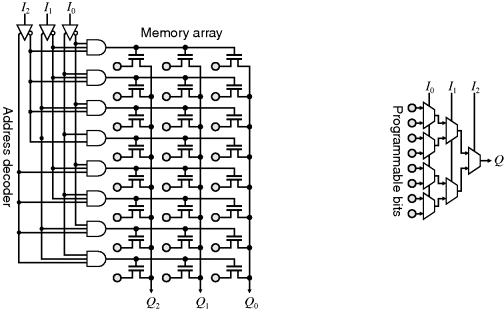
An alternative simplification to the PAL is to fix the AND section and make the OR section programmable, as shown in the right panel of Figure 2.1. This structure effectively results in a programmable read only memory (PROM) or lookup table (LUT). Each AND gate will correspond to one combination of the input signals, corresponding to exactly one line of the truth table representation of the function. So for three inputs, there will be 23 or eight AND gates. The OR section is programmed to select the combination of inputs required to give a high output. A lookup table may implement any arbitrary function of its inputs. This gives PROMs considerable flexibility, although the circuit size grows exponentially with the number of inputs, which restricts the usefulness of PROMs to where only a few inputs are required. Larger PROMs are also much slower than dedicated logic circuits, and consume more power. For these reasons, large PROMs are not often used for general programmable logic. However, the flexibility of the lookup table architecture can be effective with a small number of inputs, making it the most commonly used building block within FPGAs. In practise, a PROM is not implemented as shown in Figure 2.1. The programmable OR connection is usually replaced by a programmed memory cell, which is connected to the output via a pass transistor as shown in Figure 2.2. Alternatively, for a small number of inputs the programmed memory cell may be connected to the output via a multiplexer tree.
Figure 2.2 PROM architectures. Left: implemented as memory; right: multiplexer tree.
The programmable logic described so far only has a limited number of inputs and outputs. The next step in the development of programmable logic was to incorporate several blocks of logic on a single chip, with programmable interconnections to enable more complex logic functions to be created. Two classes of device resulted – complex programmable logic devices (CPLDs) based on the PAL architecture, and FPGAs based on the LUT architecture. These differences mean that CPLDs have a higher density of logic compared to interconnect, whereas the logic blocks within FPGAs are smaller and the architecture is more dominated by interconnects. The other main difference between CPLDs and FPGAs is that CPLDs tend to be flash-programmable, whereas the programme or configuration for most FPGAs is usually held in static memory cells. This makes the configuration volatile, requiring it to be reloaded each time the device is powered on. The configuration data is contained in a configuration file which is used to programme the system.
Both CPLDs and FPGAs were introduced in the mid 1980s, and were initially used primarily as glue logic on printed circuit boards to flexibly interconnect a range of other components. However, as device densities increased, FPGAs began to dominate because of the increased flexibility that came primarily through the more flexible interconnect structure. Current FPGAs have sufficient logic resources (and associated interconnect routing) to implement even complex applications on a single chip. More recent trends have led to the integration of specific functional blocks within the FPGA, including multipliers, memories, high speed input–output interfaces, and even serial processor cores (Leong, 2008). Implementing such commonly used features as dedicated blocks frees up the programmable logic resources that would otherwise be required. It also increases the speed and reduces the power consumption compared with implementing those functions out of general purpose programmable logic.
2.1.1 FPGAs vs. ASICs
Programmability comes at a cost, however. If an FPGA-based implementation is compared with the same implementation in dedicated hardware as an application specific integrated circuit (ASIC), the FPGA requires more silicon, is slower, and requires more power. This should not come as a surprise – a custom made circuit will always be smaller than a generic circuit for a number of reasons. Firstly, the custom circuit only needs to consist of the gates that are required for the application, whereas the programmable circuit will inevitably have components that are not used, or not used in the best possible way. Secondly, a programmable interconnect is not required in a custom circuit; the logic is just wired where it is needed. The interconnect logic must also be sufficiently flexible to allow a wide range of designs, so again it will only be partially used in any particular configuration. Thirdly, the programmable hardware requires extra configuration logic, which also consumes a significant proportion of the chip real estate. Taking all these factors into consideration, an FPGA requires 20–40 times the silicon area of an equivalent ASIC (Kuon and Rose, 2006). It is at the higher end of this range for designs dominated by logic, and at the lower end of the range for those applications that make significant use multiplier blocks and memories, where the programmable blocks are bigger.
In terms of speed, the flexibility of programmable logic means that it will always be slower than a custom circuit. Also, since programmable circuits are larger, they will have more capacitance, reducing the maximum clock speed. On custom hardware, the wiring delays can be minimised by placing connected components as close as possible to each other. The need for programmable interconnect on FPGAs means the logic blocks are spaced further apart, so it takes longer for the signals to travel from one block to another. This is made worse by the fact that designs tend to be more scattered over the resources available by the automated place and route tools. Finally, every interconnection switch that a signal passes through also introduces a delay. Therefore, an ASIC will typically be three to four times faster than an FPGA (Kuon and Rose, 2006) for the same level of technology.
An FPGA will also consume about 10–15 times more dynamic power than a comparable ASIC (Kuon and Rose, 2006). The main causes of the large disparity in power dissipation are the increased capacitance and the larger number of transistors that must be switched.
In spite of these disadvantages, FPGAs do have significant advantages over ASICs, particularly with digital systems. The mask and design costs of ASICs are significantly higher, although the cost per chip is significantly lower (Figure 2.3). This makes ASICs only economical where high volumes are required, or where the speed cannot be matched by an FPGA. With each new technology generation the capabilities of FPGAs increase, moving the crossover point to higher and higher volumes. FPGAs also enable a shorter time to market, both because of the shorter design period and because the reconfigurability allows the design to be modified relatively late into the design cycle. The fact that the design may also be reconfigured in the field can also extend the useful lifetime of a product based on FPGAs. The future is likely to see an increased use of reconfigurability within ASICs to address these issues (Rutenbar et al., 2001).
Figure 2.3 The relative costs of FPGAs, ASICs and structured ASICs.
Structured ASIC approaches, which effectively take an FPGA design and replace it with the same logic (hardwired) and fixed routing, can also overcome some of these problems. A structured ASIC consists of a predefined sea of gates, with the interconnections added later. This effectively makes them mask-programmed FPGAs. Fabrication of the user's device consists of adding from two to six metal layers forming the interconnection wiring between the gates. The initial cost is lower because the design and mask costs for the underlying silicon can be shared over a large number of devices, and only the metal interconnection layers need to be added to make a functioning device.
Both Altera (with HardCopy; Altera, 2009a) and Xilinx (with EasyPath; Krishnan, 2005) provide services based on their high end FPGA families for converting an FPGA implementation into a structured ASIC. The underlying sea of gates for these reflects the underlying architecture of the FPGA on which they are based. Such devices provide significant cost reductions for volume production, while achieving a 50% improvement in performance at less than half the power of the FPGA design they are based on (Leong, 2008). NEC Electronics Corporation also provides an embedded gate array service (NEC, 2009). This is based in a generic sea of gates, with the logic designs mapped onto these gates.
For prototyping, and designs where a relatively small number of units is required, the programmability and low cost of FPGAs makes them the device of choice.
2.2 FPGAs and Image Processing
Since an FPGA implements the logic required by an application by building separate hardware for each function, FPGAs are inherently parallel. This gives them the speed that results from a hardware design while retaining the reprogrammable flexibility of software at a relatively low cost. This makes FPGAs well suited to image processing, particularly at the low and intermediate levels where they are able to exploit the parallelism inherent in images. FPGAs can readily implement most of the forms of parallelism discussed in Section 1.8.
For a pipelined architecture, separate hardware is built for each image processing operation in the pipeline. In a data synchronous system, data is simply passed from the output of one operation to the input of the next. If the data is not synchronous, appropriate buffers may be incorporated between the operations to manage variations in dataflow or access patterns.
Spatial parallelism may be exploited by building multiple copies of the processing hardware and assigning different image partitions to each of the copies. The extreme case of spatial parallelism consists of building a separate processor for each pixel. This is not really practical for all but very small images; for realistic sized images, such massive parallelism does not map well onto current FPGAs, simply because the number of pixels within images exceeds the resources available within an FPGA.
Logical parallelism within an image processing operation is well suited to FPGA implementation, and it is here where many image processing algorithms may be accelerated significantly. This is accomplished by unrolling the inner loops, so that rather than performing the operations sequentially, parallel hardware is used.
Streaming feeds image data serially through a single function block. This maps well to a hardware implementation, especially when interfacing directly to a camera or display where the images are naturally streamed. If all of the operations are able to be implemented using stream processing, then the implementation of the whole algorithm as a single streamed pipeline results in a very efficient implementation. With stream processing, pipelining is usually required to achieve the required throughput.
The ability to make significant use of parallelism has significant implications when building embedded vision systems. Performing multiple operations in parallel enables the clock speed to be lowered significantly. A VGA resolution video streamed from a camera at 30 frames per second produces approximately 10 million pixels per second (although the clock speed is usually higher to account for the blanking periods). Any significant processing requires many operations to be performed for each pixel, requiring a conventional serial processor to have a much higher clock frequency. A streamed pipelined system implemented on an FPGA can often be operated at the native pixel input (or output) clock frequency. This corresponds to a reduction in clock speed over a serial processor of two orders of magnitude or more. The dynamic power consumption of a system is directly related to the clock frequency, so a slower clock results in a significantly lower power design.
If the whole algorithm can be implemented on a single FPGA, the resulting system has a small form factor. Designs with only two or three chips are possible, enabling the whole image processing system to be embedded with the sensor. This enables smart sensors and smart cameras to be built, where the intelligence of the system is built within the camera (Leeser et al., 2004; Mosqueron et al., 2007). The result is that vision can then be embedded within many applications as a versatile sensor.
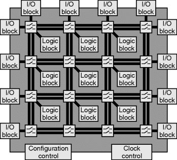
So, what exactly is inside an FPGA? Figure 2.4 shows the basic structure and essential components of a generic FPGA. The programmable logic consists of a set of fine-grained blocks that are used to implement the logic of the application. This is sometimes called the fabric of the FPGA. The logic blocks are usually based on a lookup table architecture, enabling them to implement any arbitrary function of the inputs. The logic blocks are typically tiled in a grid structure and interconnected via a programmable routing matrix that enables the blocks to be connected in arbitrary configurations. The input and output (I/O) blocks interface between the internals or core of the FPGA and external devices. The routing means that virtually any signal can be routed to any I/O pin of the device.
Figure 2.4 The basic architecture of an FPGA.
In addition to these basic features, most FPGAs provide some form of clock synchronisation to control the timing of a clock signal relative to an external source. A clock distribution network provides clock signals to all parts of the FPGA while limiting the clock skew between different sections of a design. There is also some dedicated logic for loading the configuration into the FPGA. This logic does not directly form part of the user's design, but is the overhead required for FPGAs to be programmable and provides the mechanisms for loading the user's design onto an FPGA.
Each of these components is examined in a little more detail in the following sections.
2.3.1 Logic
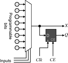
The smallest unit of logic within the FPGA is a logic cell. This is the finest grain logic unit producing a single bit output. It typically consists of a small LUT and a latch on the output, as represented in Figure 2.5. A common terminology is to refer to a three-input LUT as a 3-LUT, and similarly for other LUT sizes. The latch is used to register the output. On some FPGAs, both outputs may be provided, as in Figure 2.5; on others, a multiplexer may be used to select whether the registered or unregistered signal is output. The registers can be used for building finite state machines, counters, and for registering data within pipelined systems.
Figure 2.5 A logic cell is the basic building block of an FPGA.
The LUT can implement any arbitrary function of its inputs. More complex functions can be implemented by cascading multiple levels of LUTs by connecting the output, ![]() , to the input of the next layer. FPGA manufacturers face a trade-off in choosing the size of the LUTs. Consider implementing a simple two-input AND gate. With a large LUT, a significant fraction of the logic would be unused. Smaller LUTs would achieve a higher usage of resources. However, when implementing complex functions with small LUTs, multiple logic cells would have to be cascaded, which can significantly increase the propagation delay. For complex functions, using a larger LUT would be preferable. To balance this, the silicon area of the table grows exponentially with the number of inputs, so at some stage it is more efficient to split a complex function over multiple LUTs. A larger LUT also has a longer propagation delay than a smaller table because of the extra levels in the multiplexer tree. Early studies showed that the optimum size is for the LUT to have four to six inputs (Kouloheris and El Gamal, 1991; Singh et al., 1992). Early FPGAs used 3-LUTs and 4-LUTs. However, as device scales have shrunk, the proportion of the total propagation delay used by the routing matrix has increased. This has led to larger LUTs in more recent devices, for example recent Xilinx devices use 6-LUTs. Another approach taken is to combine two basic lookup tables, sharing some of the inputs, but allow the logic to be partitioned between the two outputs according to the application (Hutton et al., 2004).
, to the input of the next layer. FPGA manufacturers face a trade-off in choosing the size of the LUTs. Consider implementing a simple two-input AND gate. With a large LUT, a significant fraction of the logic would be unused. Smaller LUTs would achieve a higher usage of resources. However, when implementing complex functions with small LUTs, multiple logic cells would have to be cascaded, which can significantly increase the propagation delay. For complex functions, using a larger LUT would be preferable. To balance this, the silicon area of the table grows exponentially with the number of inputs, so at some stage it is more efficient to split a complex function over multiple LUTs. A larger LUT also has a longer propagation delay than a smaller table because of the extra levels in the multiplexer tree. Early studies showed that the optimum size is for the LUT to have four to six inputs (Kouloheris and El Gamal, 1991; Singh et al., 1992). Early FPGAs used 3-LUTs and 4-LUTs. However, as device scales have shrunk, the proportion of the total propagation delay used by the routing matrix has increased. This has led to larger LUTs in more recent devices, for example recent Xilinx devices use 6-LUTs. Another approach taken is to combine two basic lookup tables, sharing some of the inputs, but allow the logic to be partitioned between the two outputs according to the application (Hutton et al., 2004).
It is also usual to combine multiple logic cells into a logic block or tile, as in Figure 2.4. All of the logic cells within a block share common control signals, for example, common clock and clock enable signals. In a logic block, the outputs are directly available as inputs to other logic cells within the same block. The resulting direct connections reduce the number of signals that need to be routed through the interconnect matrix, reducing the propagation delay on the critical path. A small number of additional dedicated multiplexers allow more complex functions to be synthesised by combining adjacent LUTs to effectively create a larger LUT. Studies have shown that the optimal logic block size is four to ten logic cells (Ahmed and Rose, 2000).
Many of the early FPGAs were homogenous in that there was only one type of logic resource. However, as FPGAs developed and moved from being used primarily as glue logic to compute resources in their own right, implementing many functions using fine-grained logic was expensive. This has led to a more heterogeneous architecture, with a range of more complex coarser-grained building blocks.
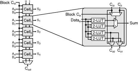
Addition is a commonly performed operation. On an FPGA, a full adder would require two 3-LUTs, one to produce the sum and one to produce the carry. With a ripple adder, the propagation of the carry signal through the routing matrix is more likely to form the critical path. Since addition is such a common operation, many manufacturers provide additional circuitry within logic cells (or logic blocks) to reduce the resources required and significantly reduce the critical path for carry propagation. This usually consists of dedicated logic to detect the carry (so only one LUT is needed per bit of addition) and a dedicated direct connection for the carry signal between adjacent logic cells.
Multiplication is also a common operation in digital signal processing (DSP). A multiplier can be implemented using logic blocks to perform a series of additions, either sequentially or in parallel. Sequentially, multiplication is time consuming, requiring one clock cycle for each bit of the multiplier to perform the associated addition. Implementing the multiplication in parallel improves the timing, but consumes significant resources. Therefore, it is common in FPGAs targeting DSP and other compute intensive applications to have dedicated multiply or multiply and accumulate blocks.
On a fine-grained FPGA, all of the storage is within the flip-flops in the logic cells. While this is suitable for data that is accessed frequently, the storage space is limited, making it expensive for storing larger volumes of data. Rather than require the use of off-chip memories, many FPGAs have had small blocks of memory added on-chip for intermediate storage and buffers. This can be implemented in two ways – either by adding dedicated memory blocks (block RAM) or by adapting the structure of the logic cells to enable them to be used as a random access memory rather than as LUTs; such memory is called fabric RAM because it is made from the “fabric” of the FPGA. A high bandwidth is maintained by keeping the memory blocks small, enabling independent access to each block. Many of the memory blocks are also dual-port, simplifying the construction of FIFO buffers and custom caches. True dual-port allows independent reading and writing on each of the ports. Some memories are only simple dual-port, where one port is write only and one port is read only.
Often, some parts of an application benefit from the parallelism offered by an FPGA, and other parts are more efficiently implemented using a serial processor. In these latter cases, a serial processor may be constructed from the fabric of the FPGA. The delays associated with programmable logic and interconnect will limit the clock speed of such a processor. Therefore several high end FPGA families implement a high performance serial processor as a hardware block on the FPGA.
To summarise, fine-grained homogenous FPGAs consist of a sea of identical logic blocks. However, most current FPGAs have moved away from this homogenous structure, with a heterogeneous mixture of both fine-grained logic blocks and larger coarse-grained blocks targeted for accelerating commonly used operations. This has both advantages and disadvantages in terms of design. Heterogeneous systems will generally be faster because the coarse-grained blocks will not have the same level of overhead that comes with fine-grained flexibility. However, heterogeneous devices are also harder to programme, and if the mix of specialised blocks is not right much of the functionality may remain underused.
2.3.2 Interconnect
The purpose of the programmable interconnect is to flexibly enable the different logic blocks to be connected to implement the desired functionality. Obviously it is impractical to provide a dedicated direct connection from every possible output to every possible input. In any given application, only a very small fraction of these connections would be required; however, any of the connections potentially may be required. The solution is to have a smaller set of connection resources (routing lines) that can be shared flexibly to create the connections required for a given application, a little like the cables in a telephone network.
Since the interconnect takes up room on the silicon, there is a compromise. If only a few routing lines are provided, more space is available for logic, but complex circuits cannot be constructed because of insufficient interconnection resources. Alternatively, if too many routing lines are provided, many will not be used, and this reduces the area available for logic. There is an optimum somewhere in between these extremes, where sufficient routing lines are available for most applications, without using too much space.
The connection network for most FPGAs is based on a grid structure, similar to that shown in Figure 2.4. At each grid intersection some form of crossbar switch enables programmable connection between the horizontal and vertical routing lines.
Another factor that needs to be considered is the propagation delay through the interconnection network. Each switch that the signal passes through will add to the delay. This has led to a segmented structure, where not every routing line is switched at every junction. Also, dedicated direct connections can be provided between adjacent logic blocks to reduce the number of signals that need to go via the interconnect matrix. While having a range of different interconnection resources improves the flexibility and speed, it can make the process of finding good routes significantly more complex, especially for designs which use most of the logic available on the FPGA.
It is important that only a single output is driving a routing line. If two outputs are connected together, with one high and the other low, the power supply will effectively be shorted, causing damage to the chip. One of the roles of the FPGA programming tools is to ensure that this never happens. Devices that use bus structures for routing must limit the current of driving transistors, or use open drain and passive pull-up. Both approaches affect the speed and power dissipation.
2.3.3 Input and Output
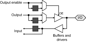
Input and output blocks enable the connection of signals between the FPGA and external devices. The flexibility of FPGAs requires them to be able to connect to a wide range of other components. Most of the I/O pins can be programmed as inputs, outputs, or both, and be connected directly to the internal logic of the FPGA, or pass via registers. This range of functionality may be provided by a generic I/O block such as that shown in Figure 2.6, with each multiplexer controlled by a programmable configuration bit. The main complexity of I/O arises from the large number of different signalling standards used by different devices and ensuring appropriate synchronisation between the FPGA and the off-chip components.
Figure 2.6 Generic input/output block.
Perhaps the most common signalling standard is Low Voltage Transistor–Transistor Logic (LVTTL) or Low Voltage CMOS (LVCMOS), which are suitable for general purpose 3.3V signals. FPGAs will almost certainly require a separate power supply for the I/O pins because the I/O voltages are often larger than the core supply voltage. Some standards may also require an external voltage reference to determine the threshold level between a logical 0 and 1. The voltage supply and reference levels will usually apply to a group or bank of I/O pins.
It is important when interfacing high speed signals to consider transmission line effects. A general rule of thumb is that any connection longer than about one-eighth of the rise time should have appropriate termination to minimise signal reflections. As FPGAs have become larger and faster, it has become common practise to provide programmable on-chip termination. If not provided, it is necessary to ensure that appropriate termination is built off-chip for fast switching signals.
Just as dedicated logic blocks are provided in some FPGAs for commonly used functions, many newer FPGAs may also include dedicated I/O hardware to manage some commonly used connections and protocols. One example is the logic required to interface to double data rate (DDR) memories. Two data bits are transferred per clock cycle on each I/O pin, one on clock high and one on clock low. Multiplexing and de-multiplexing are built into the I/O block, enabling the internal circuitry to operate at the clock rate rather than twice the clock rate. Differential signalling is commonly used for high speed communication because it is less sensitive to noise and cross-talk. This improved noise immunity enables a lower signalling voltage to be used, reducing the power requirements. Most of the recent FPGAs include the logic for managing low voltage differential signalling (LVDS), which requires two I/O pins for each bit.
High speed serial standards have signalling rates higher than the maximum clock speed supported by the core of the FPGA. Support for such standards requires incorporation of parallel-to-serial converters on outputs and serial-to-parallel converters on inputs. The serialisation and deserialisation (SERDES) logic enables the FPGA to run at a lower speed than required by the communication data rate.
Many high level communication protocols would require significant FPGA resources simply to manage the protocol. While this can be implemented in the fabric of the FPGA, the design is often quite complex and is better implemented using a dedicated interface chip. Such chips typically manage the media access control (MAC) and physical signalling (PHY) requiring only standard logic signals in their interface with the FPGA. Some FPGAs incorporate dedicated MAC and PHY circuitry for commonly used communications protocols, such as PCI express and Gigabit Ethernet.
Most FPGAs provide a range of both general purpose and dedicated I/O connections.
2.3.4 Clocking
FPGAs are designed primarily as synchronous devices, so require a clock signal. Although multiple clocks may be used in a design, registers, synchronous memories and I/O blocks can only be controlled by one clock. A clock domain consists of all the circuitry that is controlled by a particular clock.
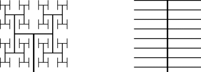
Since a clock drives a lot of inputs potentially over the whole of the FPGA, there are two special characteristics of clock lines that distinguish them from other interconnections on an FPGA. Firstly, it is important that all registers in a clock domain are clocked simultaneously. Clock skew is the difference in arrival time of the clock signal at successive registers in a design (Friedman, 2001). Any skew will reduce the timing margin and impact the maximum clock speed of a design. Although skew can be minimised by using H-tree or X-tree clock distribution networks, these do not fit well with the grid based structure of FPGAs (Lamoureux and Wilton, 2006). Instead, a spine and ribs structure is typically used (Figure 2.7), where the clock is distributed to rows using a spine and then to the elements on the row using the ribs (Lamoureux and Wilton, 2006). A series of buffers is used within the distribution network to manage the high fan-out. In practise, it is a little more complex than this, as the network must cater for multiple clock domains, and many FPGAs also have a mixture of local clocks and global clocks.
Figure 2.7 Clock distribution networks. Left: H-tree structure; right: spine and ribs structure.
Delay locked loops (DLLs) are used to minimise the skew and to synchronise clocks with external sources. These dynamically adjust a programmable delay to align the clock edge with an external reference. A side effect is making the output duty cycle 50% and providing quadrature phase clock signals. While the delay locked loop will match the input frequency, phase locked loops (PLLs) can also be used to synthesise different clock frequencies by multiplying a reference clock by an integer ratio.
2.3.5 Configuration
All of the switches, structures and options within the FPGA are controlled by configuration bits. Most commonly, the configuration data is contained within the FPGA in static memory (SRAM) cells, although flash-programmed devices are available from some manufacturers. Flash-programmed FPGAs are non-volatile, retaining their configuration after power-off, so they can immediately begin working after powering-on. Static memory based FPGAs lose their configuration on power-off, requiring the configuration file to be reloaded every time the system is powered on. Static memory had the advantage of being infinitely reprogrammable; flash memory typically has a limited number of write cycles.
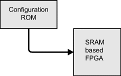
An FPGA is configured by loading the configuration file into the internal memory. This is usually accomplished by streaming the configuration file onto the FPGA either serially, or in parallel 8, 16 or in some cases 32 bits at a time. In a stand-alone system, the configuration file is usually contained within an external flash memory, such as that shown in Figure 2.8, with the board set up to automatically configure the FPGA on power-on. FPGAs can also be programmed serially via a JTAG (Joint Test Action Group) interface, and this interface is commonly used when programming an FPGA from a host computer system. The need to transfer the configuration into the FPGA each time the system is powered exposes the configuration file making the intellectual property contained within vulnerable to piracy or reverse engineering. The higher end FPGAs overcome this limitation by encrypting the configuration file and decrypting the configuration once it is within the FPGA.
Figure 2.8 Configuration of static RAM-based FPGAs.
FPGAs can also be reconfigured at any time after power-on. Since the configuration controls all aspects of the operation of the FPGA, it is necessary to suspend operation and restart it after the new configuration is loaded. No state information can be retained from one configuration to the next – all of the flip-flops are reset and all memories are usually initialised according to the new configuration. Therefore, any state information must be saved off-chip and reloaded after reconfiguration.
Some FPGAs can be partially reconfigured. The internal static memory controlling the configuration is addressed via internal registers, allowing the configuration for part of the FPGA to be accessed and changed. As before, this cannot be done while that part of the FPGA is operating; however, the rest of the FPGA can continue executing normally. Partial reconfiguration requires the layout of the design to be structured in such a way that the blocks being reconfigured are within a small area on the FPGA to facilitate loading at run-time.
Some FPGAs also support read-back of the configuration from the FPGA. This feature can be useful for debugging a design, given appropriate tools, but is generally not used in normal operation.
2.3.6 Power Consumption
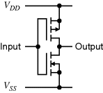
In embedded applications, the power consumption of the system, and in particular of the FPGA, is of importance. The power dissipated by an FPGA can be split into two components: static power and dynamic power. Dynamic power is the power required for switching signals from 0 to 1 and vice versa. Conversely, static power is that consumed when not switching, simply by virtue of the device being switched on. Most FPGAs are based on CMOS technology. A CMOS inverter, the most basic CMOS circuit, is shown in Figure 2.9. It consists of a P-channel pull-up transistor and an N-channel pull-down transistor. Only one of the transistors is on at any one time, and since the MOS transistors have a very high off-resistance, CMOS circuits typically have very low static power dissipation.
Figure 2.9 CMOS inverter.
Any significant power is only dissipated when the output changes state. This results from two main sources (Sarwar, 1997). The first is from charging the capacitance on the output line. The capacitance results from the inputs of any gates connected to the output, combined with the stray capacitance associated with the wiring between the output and any downstream inputs. The power required is given by
where ![]() is the average number of outputs that are changing in each clock cycle,
is the average number of outputs that are changing in each clock cycle, ![]() is the average capacitance on each output and
is the average capacitance on each output and ![]() is the clock frequency. For an embedded system, the power consumption may be reduced by considering each of the terms of Equation 2.1:
is the clock frequency. For an embedded system, the power consumption may be reduced by considering each of the terms of Equation 2.1:
- by limiting the number of outputs that change with each clock cycle;
- by minimising the fan-out from each gate and minimising the use of long wires (to keep the capacitance lower);
- by reducing the power supply voltage (although the developer has little control over this, it has been reducing with each technology generation); and
- by reducing the clock frequency.
In terms of a given design, reducing the clock frequency probably has the most significant effect on reducing the power consumption, as it is often the clock signal itself that dissipates the most power. It is toggling with every cycle, and because the clock distribution network extends over the whole FPGA it also has a high capacitance. Minimising the number of clock domains and keeping the logic associated with each clock domain together can also help to limit the power used by the clock circuitry.
The second component of dynamic power dissipation results from the fact that as one transistor is switching off, the other is switching on. During the transition there is a brief interval when both transistors are partially on and there is a conduction path between ![]() and
and ![]() . For fast transition rates, power dissipation from this source is typically much lower than that from charging the load capacitance. The flow-through current can be minimised by keeping the input rise time short, which can be managed by limiting the fan-out from the driving source. This flow-through current is becoming more important with reducing
. For fast transition rates, power dissipation from this source is typically much lower than that from charging the load capacitance. The flow-through current can be minimised by keeping the input rise time short, which can be managed by limiting the fan-out from the driving source. This flow-through current is becoming more important with reducing ![]() because the threshold voltages of the P- and N-channel transistors are brought closer together and both transistors are partially on for a wider proportion of the input voltage swing.
because the threshold voltages of the P- and N-channel transistors are brought closer together and both transistors are partially on for a wider proportion of the input voltage swing.
The static power dissipation arises from leakage currents from five different sources (Unsal and Koren, 2003) of which the subthreshold leakage is dominant. This is the leakage current through the transistor when the gate voltage is below the switching threshold and the transistor should be switched off. As the feature size and supply voltage of devices is scaled down, the threshold voltage must also be scaled down to maintain device speed. Unfortunately, the subthreshold leakage current scales exponentially with decreasing threshold voltage, so the leakage current contributes to an increasing proportion of the total power dissipation with each technology generation (Kao et al., 2002; Unsal and Koren, 2003).
Several techniques can mitigate against this increase in subthreshold leakage current (Kao et al., 2002). One is to use a higher threshold voltage in the sections of the circuit where the speed is not critical, and only use low threshold devices on the critical path. Another technique is to switch off sections of the circuit which are not being used, or at least place them on standby. Both of these techniques are used by FPGA manufacturers.
The user's design can significantly affect the power dissipated by an FPGA. In general, minimising the clock frequency and minimising the number of signals that transition every clock cycle can significantly reduce power dissipation. There may be limited control over the length of the interconnections, as much of this is managed automatically by the vendor's place and route tools. However, these tools are also programmed to minimise the length of the interconnections.
Another factor that can influence the design of embedded systems is the large current burst drawn from the power supply when the device is switched on. This results from the activity that takes place as the FPGA is configured. It is essential that the power supplies be able to handle this peak current, and not just the average required for normal operation. This is of particular concern in low power, battery operated devices where the peak current may be limited.
2.4 FPGA Families and Features
In the previous section the architectural features of FPGAs were reviewed in a general way. In this section, the particular characteristics of devices from several manufacturers are considered in more detail. The two main FPGA manufacturers in terms of market share are Xilinx and Altera, although there are several others that provide FPGAs. The current offerings from each of these are described in turn. Of particular interest from an image processing perspective is the size of the device in terms of logic resources, embedded memories, embedded multipliers or DSP blocks, and whether or not the device includes a processor core. (Note, where a processor core is not available, it is still possible to implement a soft processor using the logic resources.) For each family the range of resources across the different family members is listed. In the number of logic cells, 1 k represents 1000 cells. The RAM size is given in bits, where 1 K = 1024 bits. The total RAM figures represent the dedicated block RAM available on the FPGA, and do not include fabric RAM. The descriptions given are by necessity brief; more details may be found in the data sheets or product guides referred to; these are available from the manufacturer's web sites.
2.4.1 Xilinx
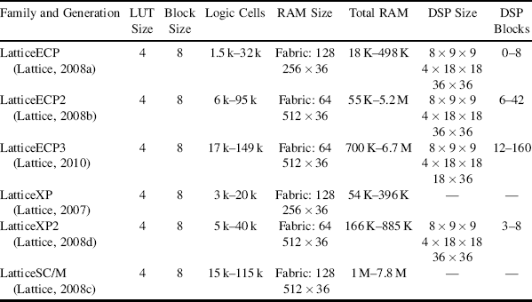
Xilinx was one of the first developers of field programmable gate array technology. It has had a number of families of devices, with the two current families being the Spartan series and the Virtex series. The main difference between the two families is that the Spartan devices are designed primarily for low cost, and the Virtex devices are designed primarily for high performance. Both families are discussed here chronologically, outlining the key features that have been added with each succeeding generation. In the newest generation, the 7 Series devices, the Spartan family is replaced by the Artix and Kintex families. Within each generation, a range of device sizes is available. The key characteristics are summarised in Table 2.1 with more details to be found from the data sheets (the shaded lines in the table represent “mature” devices that are no longer recommended for new designs).
Table 2.1 Characteristics of the Xilinx FPGA families.
2.4.1.1 Virtex and Spartan-II
Although the Virtex and Spartan-II are now obsolete, it is instructive to look at their architecture to see the evolution with successive generations. Both the Virtex and Spartan-II are structurally similar, so will be described together.
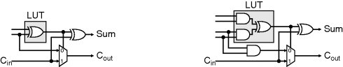
The basic logic cell is a 4-LUT. Each logic cell also has a flip-flop on the output. However, a bypass input is also provided allowing the LUT to be bypassed, enabling the LUT and flip-flop to be used independently. A dedicated multiplexer combines the outputs of two adjacent logic cells to implement a 5-LUT or a 4:1 multiplexer. (Xilinx calls this pair of logic cells a slice.) Another multiplexer enables two slices to be combined, to implement a 6-LUT or 8:1 multiplexer. Additional logic is provided to accelerate arithmetic operations. The carry chain includes multiplexers for carry generation and propagation, along with an XOR gate to enable a full adder to be implemented within a single logic cell, as demonstrated in Figure 2.10. The carry chain propagates vertically up the columns within the FPGA. Each logic cell also provides a dedicated AND gate to reduce the logic required to implement multiplication.
Figure 2.10 Left: logic required to implement a full adder with a single logic cell; right: a two-bit multiplication in a single logic cell. (Adapted from Elzinga et al. (2000); reproduced by permission of Xilinx, Inc.)
Each logic cell can also be configured as a 16 × 1 bit fabric RAM or as a 16-bit shift register. The two logic cells within a slice may be combined to implement a dual-port memory. This fabric RAM is useful for storing coefficients or other small data structures where the memory depth is shallow. In addition to the fine-grained fabric RAM, both the Virtex and Spartan-II contain blocks of dual-port memory, where each block contains 4096 bits. The aspect ratio may be configured between 4096 × 1 to 256 × 16, making it useful for implementing row buffers and larger FIFO buffers.
There is a range of interconnection resources between the logic blocks. There are direct connections within a logic block and to adjacent logic blocks horizontally, enabling the logic cells to be chained efficiently. In addition to the direct connections, the routing matrix provides four types of connections:
- single length lines connecting adjacent tiles, both horizontally and vertically;
- hex lines that span six tiles, with a connection after three tiles;
- buffered long lines that span the whole chip, both horizontally and vertically; and
- horizontal bus lines. These can be driven by tri-state buffers within the logic blocks.
In addition to these, there are global routing resources to distribute several clocks and other global signals (such as reset) with low skew. The clock drivers use a delay locked loop to synchronise skew free to either an external or internal source. The drivers can also divide down the signal or provide multiple phases if necessary.
Configuration of the FPGA is based on a frame structure, where each frame is associated with a column (or part of a column) within the FPGA. This enables partial reconfiguration of the FPGA, on a frame by frame basis. The configuration can also be read back from the FPGA for verification or debugging. Readback will also read the contents of any user registers (the flip-flops within I/O blocks or logic cells), and RAM (both fabric RAM and block RAM).
2.4.1.2 Virtex-II
Many of the changes in moving to the Virtex-II were relatively minor. The structure of each logic cell was basically unchanged, although a logic block is now made up of eight logic cells grouped in four slices of two logic cells each. As before, the logic cells may also be configured as fabric RAM or shift registers. An additional OR gate was added per slice to enable implementation of large sum of products chains (Xilinx, 2007b). Each logic cell can be configured as a 4-input AND gate, with the carry chain used to parallel adjacent logic cells to give wider input AND gates. The OR is placed at the top of each slice and can be linked horizontally to arbitrary widths. Dedicated multiplier blocks (18 × 18) were introduced with the Virtex-II, accelerating DSP and other compute applications.
The size of the block RAMs was increased to 18 Kbits, with configurable aspect ratio from 16 K × 1 to 512 × 36. The extra bits can be can be used as additional storage, although they are intended as parity bits. However, the user is required to implement any parity generation and checking logic.
There was a small change to the hierarchical routing resources. The single lines were replaced with double lines which connect over one or two tiles, both horizontally and vertically. The direct connections were also extended to allow direct connection to diagonally adjacent logic blocks.
The clock network was also augmented with local clocks associated primarily with I/Os. The clock drivers were augmented to include phase locked loops to enable frequency synthesis by a ratio of integers. The I/O blocks were enhanced to provide digitally controlled termination and direct support for differential I/O and double data rate standards.
The Virtex-II Pro added a number of additional coarse-grained blocks (Xilinx, 2007b). A key new feature was the introduction of a PowerPC processor core to accelerate high performance computing applications. Another new feature to facilitate high speed communication was the multigigabit transceiver cores (called RocketIO by Xilinx). These cores include SERDES logic to enable the communication to take place at a much higher clock speed than is used internally for the logic.
2.4.1.3 Virtex-4 and Spartan-III
The previous generation of FPGAs saw an increase in the use of coarser grained block for implementing specific functions. However, different applications require a different mix of these blocks. For example DSP applications make extensive use of hardware multiplication; communication applications require the high speed connectivity; image processing makes extensive use of the internal RAM for buffering. Therefore, to provide a good mix of features targeted at specific application areas, Xilinx provides several FPGAs within each family that have a different mix of coarse-grained blocks. From an image processing perspective, of particular interest are the devices that provide a focus on logic, block memories, and in some imaging applications, DSP resources.
The biggest change within the logic blocks is that only half of the slices may now be used as fabric RAM or as a shift register. All of the slices within a logic block still have fast carry chains. All of the devices have multiplier blocks, although the Virtex-4 devices also include a 48-bit post-adder and accumulator, and the Spartan-III add to this an 18-bit pre-adder on one of the multiplier inputs. Both families use 18 Kbit block RAMs, although the Virtex 4 also provides built-in logic to operate the block RAM as a FIFO without using additional logic resources.
The interconnect resources are the similar to those provided with the previous generation devices. Two notable exceptions are that the long lines only connect to every sixth tile, and the horizontal busses and associated tri-state buffers are no longer provided.
The clock managers introduced with the Virtex-II have been extended to the Spartan family as well. Similarly, the programmable I/O termination, support for differential signalling and double data rate interface have been extended to both families.
The Virtex-4 FX branch also includes the PowerPC core, high speed transceiver blocks and an Ethernet MAC. The Virtex-4 also introduces an internal configuration access port that makes the configuration memory of the clock managers and high speed I/O ports accessible from internal to the FPGA. This enables these devices to be reconfigured directly from within the fabric of the FPGA, or through the embedded processor. Also introduced with the Virtex-4 is encryption of the configuration file to prevent the design from being copied or reverse engineered. The decryption key is stored in volatile memory, which requires a battery backup to retain when the system is powered off.
The Spartan-3AN includes a serial flash memory on chip that can be used to configure the FPGA (Xilinx, 2009b). This has sufficient capacity for two complete configuration files, plus additional capacity for user applications.
2.4.1.4 Virtex-5
In the Virtex-5, the size of the logic cell increased to a 6-LUT, which may be fragmented to two 5-LUTs (sharing common inputs). The logic block architecture has four LUTs per slice, and two slices per logic block. As with the Virtex-4, only one of the slices can be configured as fabric RAM or a shift register. However, the increase to four LUTs per slice allows the fabric RAM to be configured as quad-port (using all four logic cells as separate interfaces), although only one port has read and write capability; the other ports are read only. A logic cell can be configured as a programmable 32-bit or dual 16-bit shift register.
The size of the block RAMs has been increased to 36 Kbits per block. The aspect ratio may be configured from 32 K × 1 to 1024 × 36 as full dual-port, or as 512 × 72 simple dual-port. The block can also be partitioned as two independent 18 Kbit memories. Optional 64-bit error correction circuitry is built in, enabling detection of 2-bit errors and correction of single-bit errors.
New to the Virtex-5 are PCI express endpoint blocks in some branches of the family. This can simplify connection with other devices, or a host computer through the PCI express interface.
2.4.1.5 Virtex-6 and Spartan-6
The latest members of the Xilinx FPGA families available at the time of writing are the Spartan-6 and Virtex-6. These extend the storage per logic cell to two flip-flops. While all of the logic cells within the Virtex-6 provide arithmetic logic and carry chains, only half of those within the Spartan-6 do so. Similarly, approximately half of the Virtex-6 logic cells can be used as fabric RAM or shift registers, while only approximately one quarter of the Spartan-6 logic cells can be configured to do so.
The interconnect model within the Spartan-6 has also been changed to give more focus on local routing. The horizontal and vertical long-lines have been removed, with the following resources now available (Xilinx, 2010b):
- direct connections back to the inputs within the same logic block;
- single hop, to adjacent tiles horizontally and vertically;
- double hop, to two tiles away horizontally and vertically, or one tile diagonally;
- quad hop, to four tiles away horizontally and vertically, or two tiles diagonally.
While the Virtex-6 block RAMs have integrated FIFO logic and support for error correction, this has not been migrated to the Spartan family. However, new with the Spartan-6 is an integrated memory control block that simplifies the interface to common memory types. This transparently hides the buffering and control with high speed high bandwidth DDR connections (Xilinx, 2010c). The PCI express endpoint blocks and high speed transceivers previously only present in the Virtex family have now been migrated to some of the Spartan-6 FPGAs. It is interesting that Xilinx has not continued the FX series with the PowerPC processor into the Virtex-6 generation.
2.4.1.6 Virtex-7, Artix-7 and Kintex-7
Xilinx has recently announced its 7 Series of devices. This latest generation of Xilinx FPGAs all share a common underlying architecture, designed to simplify the portability of a design from one family to the other. At the logic level, the Xilinx-7 Series is similar to the Virtex-6, but implemented in an advanced 28 nm process technology. This gives improved performance while at the same time giving significant power savings over previous generations. The main differences between the families are the size of the devices and the target market. The Artix-7 family is optimised for low cost and power and is designed with a small footprint targeting high volume embedded applications. As before, the Virtex-7 family is targeted for highest performance and capacity. The Kintex-7 family sits between the other two families, giving a balance between cost and performance.
A new feature added with the 7 Series is a general purpose analogue to digital converter that gives 12 bits resolution at up to one mega-samples per second. While too slow for video, these A/D converters would be useful in many embedded control applications.
2.4.2 Altera
Altera currently provides three families of FPGAs: the low cost Cyclone series, the mid range Arria series and the high performance Stratix series (Table 2.2). The original Stratix used the same logic architecture as the Cyclone, but with the Stratix II Altera introduced a new adaptive logic module (Hutton et al., 2004). None of the current families incorporate a processor core within the logic; the last to do so was the Excalibur FPGA, based on the now obsolete Apex20K family. In terms of embedded processors, Altera has focussed its efforts on its soft-core NIOS processor. However, the Excalibur is included in Table 2.2 for comparison.
Table 2.2 Characteristics of the Altera FPGA families.
2.4.2.1 Cyclone
The Cyclone series was designed for low cost applications, making it well suited for commodity embedded devices. This includes embedded image processing applications, especially distributed vision systems where a large number of sensors is required.
The basic logic cell is a 4-LUT with a register on the output. However, for arithmetic operations, the 4-LUT is partitioned into four 2-LUTs, enabling a full adder to be implemented using a single logic cell. Both the sum and the carry are implemented efficiently as a carry-select adder, with two 2-LUTs calculating each the sum and carry on the input signals, both without and with carry. These outputs are multiplexed by the carry-in, as demonstrated in Figure 2.11. This speeds up the addition or subtraction of wide operands because the LUTs are not in the critical path and the carry signals are generated in parallel for each section. A logic block consists of ten logic cells arranged vertically in a column.
Figure 2.11 Carry select adder as implemented by Altera. (Adapted from Altera, 2008b; reproduced by permission of Altera Corporation. Altera is a trademark and service mark of Altera Corporation in the United States and other countries. Altera products are the intellectual property of Altera Corporation and are protected by copyright laws and one or more U.S. and foreign patents and patent applications.)
In addition to the logic blocks, there are also blocks of dual-port memory, with 4608 bits per block. The aspect ratio of each port can be configured from 4096 × 1 up to 128 × 36, although the largest width is only available as simple dual-port. Each memory block can also be configured as a bank of tapped shift registers, with up to 36 outputs from a combination of taps and parallel registers.
Associated with each logic block is a local interconnect, which connects between logic cells within a block, or between adjacent blocks in the same row. More distant connections are made by driving horizontal and vertical lines which extend to the local interconnects of other logic blocks up to four tiles away.
In addition to the local data interconnects, there is a global clock network, which distributes up to eight clocks throughout the FPGA. The Cyclone has two phase locked loops, which can be used to synthesise clock signals by multiplying a signal by a ratio of integers. The PLL can also provide a programmable phase shift.
The basic I/O structure of the Cyclone is similar to that in Figure 2.6. A group of I/O blocks has a local interconnect in much the same way as the logic blocks, and it is primarily through this that the I/Os are connected to the logic. Selected I/Os have integrated circuitry to interface to DDR memories. Differential signalling support is also provided, although with an external resistor network for providing appropriate termination.
Configuration is based on a SRAM cell, which is programmed by serially loading the configuration data, either through dedicated pins or through the JTAG interface. The Cyclone FPGAs are not partially reconfigurable; the complete configuration must be loaded.
2.4.2.2 Stratix
The basic structure of the Stratix FPGA is similar to that of the Cyclone. The logic block also consists of ten 4-LUTs, with local interconnect. The biggest difference is the inclusion of DSP blocks, and a wider range of memory block sizes.
Each DSP block consists of a 36 × 36 bit multiplier. One of the unique features of this multiplier is that it can be segmented, enabling four parallel 18 × 18 multiplications, or eight parallel 9 × 9 multiplications. This latter feature is particularly useful for image processing, where 9-bit multiplications are suitable in many image processing operations. The 18 × 18 and 9 × 9 multiplications can operate with an associated 52-bit accumulator, making them suitable for DSP applications.
In addition to the 4608-bit memory block provided by the Cyclone, the Stratix also provides 576 bit and 72 Kbyte blocks. A 576-bit memory may be configured with aspect ratios from 512 × 1 to 32 × 18, with separate independent read and write ports. The two ports can be of different widths and in different clock domains, enabling them to be used as small FIFO buffers, or converting between parallel and serial data for lower speed serial I/O. The 72 Kbyte sized dual-port blocks can be configured with aspect ratios from 64 K × 9 up to 4 K × 144 (although the largest data width is only simple dual-port). This makes them suitable for storing larger data tables, or even buffering part of an image. Having a range of memory sizes enables the best size to be selected for an application without wasting too many resources.
The interconnect matrix of the Stratix extends that of the Cyclone by adding additional higher speed lines that span eight rows or columns from a logic block, and high speed lines that span 24 tiles horizontally or 16 columns vertically. The clock network is also significantly enhanced, with 16 global clocks and a number of regional clocks which drive each quarter of the FPGA. These enable up to 48 independent clock domains to be implemented on the FPGA. The phase locked loops of the Stratix can be reconfigured on-the-fly, enabling the clock frequencies and delays to be dynamically adjusted by an application.
The Stratix provides direct support for double date rate (DDR) memories and quad data rate (QDR) memories with two reads and two writes per clock cycle. This simplifies interfacing to external high speed memories. On-chip termination is provided for differential signalling, with dedicated high speed SERDES blocks for high speed serial signalling.
In addition to the serial configuration modes of the Cyclone, the Stratix can also be reconfigured in parallel, significantly reducing the configuration time, especially for the larger devices. It also has a register which can be used to control which of up to eight configurations is loaded, supporting dynamic update and reconfiguration of the FPGA with a small number of components. Partial reconfigurability is limited to reprogramming the phase locked loops.
2.4.2.3 Cyclone II, III and IV
The successive generations of the Cyclone family are based on much the same architecture as the original Cyclone. The basic logic cell is still a 4-LUT with a register on the output, although the logic block is extended to 16 logic cells. However, the use of the logic cell for performing arithmetic has been changed. Rather than use the carry select adder of the original Cyclone, a simpler ripple carry adder is used. The logic cell is split into two 3-LUTs; one implements the sum and the other the carry. The carry-out connects directly to the carry-in of the next logic cell in the chain.
The new generations incorporate dedicated hardware multiplication blocks. These are not as fully featured as the DSP blocks within the Stratix series, but accelerate designs where small multipliers are used. Each multiplier block can perform a single multiplication of two 18-bit numbers, or two multiplications of 9-bit numbers.
In the Cyclone II, the embedded memory blocks are the same size as the Cyclone. However, the Cyclone III and IV double the size of each block RAM to 9 Kbits. This can be configured with aspect ratios from 8 K × 1 to 256 × 36, although only simple dual-port is supported with the widest memory.
The interconnect with the original Cyclone was restricted to short local distances. These have been extended in the later generations to include higher speed horizontal lines which span 24 tiles, and vertical lines which span 16 tiles.
With each generation, the number of PLLs and global clock lines increases. The Cyclone III extends the size of the PLL multiplier and divider from 32 to 256, and the Cyclone IV extends this further to 512. This enables finer resolution clock frequencies to be synthesised with each succeeding generation. Both the Cyclone III and IV allow the PLLs to be reconfigured at run-time without having to reconfigure the entire FPGA.
The performance of the I/O blocks improves with each succeeding generation. The Cyclone III introduces programmable on-chip termination of outputs, although inputs still require external termination. From the Cyclone II onwards, support for memory interfaces is extended to QDR memories. PCI express is also supported, although this requires an external PHY and an internal soft intellectual property core (available from Altera) to implement the required endpoint logic in the FPGA. The Cyclone IV GX introduces up to eight high speed transceivers, with SERDES logic built into the I/O block. Also included within the Cyclone IV GX is a hard-wired endpoint for PCI express, including the buffering and control logic and PHY-MAC layer.
From the Cyclone II, the configuration data can be compressed to reduce the configuration file size by up to 55%, depending on the complexity of the design and device use. The FPGA then decompresses the data as it is streamed into the FPGA. This can reduce reconfiguration times by up to a factor of two. Configuration compression is only supported with serial reconfiguration. The Cyclone III and IV also provide the option of parallel configuration, up to 16 bits per clock cycle.
2.4.2.4 Stratix II, III and IV
With the Stratix II, Altera replaced the standard 4-LUT logic cell with an adaptive logic module (ALM) (Hutton et al., 2004). The key idea behind the adaptive logic module is that when a large LUT is used, much of the logic is often unutilised. By being able to adaptively adjust the effective size of the LUTs, the logic resources within the logic cell may be better used. This increases the effective logic density without a significant penalty in terms of chip area and routing overhead. It also has the advantage that larger functions which share common inputs may be packed within a single adaptive structure. In the Stratix II ALM, up to eight inputs may be combined with two adaptive LUTs to produce two outputs. The various combinations are (Altera, 2007):
- two independent 4-LUTs;
- a 5-LUT and 3-LUT within independent inputs;
- a single 6-LUT;
- two independent 5-LUTs, with two inputs shared between the LUTs;
- two 6-LUTs with the same function, with four inputs shared between the LUTs.
As well as the adaptive LUTs, each logic cell also contains two full-adders, enabling two result bits to be generated by each logic cell. Both the LUTs and adders may be used in a design, for example to apply logic to the inputs before adding, or even to use the result of the addition to select one of the inputs. This enables, for example, three input adders to be constructed, or very efficient implementation of functions such as (Altera, 2007):
(2.2) ![]()
The outputs from the logic cell (from either the LUTs or the adders) can be optionally registered, with two registers per logic cell. The Stratix II has eight ALMs per logic block; this is increased to ten for the Stratix III and IV.
In the Stratix II, the ALMs can only implement logic. From the Stratix III on, some of the logic blocks can be configured as simple dual-port fabric RAMs. In the Stratix III, a logic cell may be configured as a 16 × 2 RAM, whereas in the Stratix IV it can be configured as a 64 × 1 RAM. The fabric RAM replaces the small 576-bit memory blocks that were available in the Stratix and Stratix II. The size of the other memory blocks was also changed with the Stratix III and IV. The size of the intermediate blocks was doubled, implementing RAMs from 8 K × 1 to 256 × 36. The size of the large blocks was reduced significantly, with each block implementing sizes from 16 K × 8 up to 2 K × 72. Again, the block memories are true dual-port except for the widest data words, where only simple dual-port is supported. Although parity bits are provided, if they are to be used for error detection and correction the user must provide the appropriate logic. The Stratix IV provides a hardware block for setting the parity bits and correction of single bit errors when the block RAM is 64 bits wide.
The architecture of the multipliers in the Stratix II is much the same as those in the original Stratix, although rounding and saturation units were introduced. These can significantly reduce the logic required to manage overflow in particular. In the Stratix III the multipliers were redesigned to natively support 9 × 9, 12 × 12, 18 × 18 and 36 × 36 multiplications. The DSP blocks can also be configured to provide a 54 × 54 bit multiplier to support double precision floating point multiplication. However, rounding and saturation logic is only provided on 18-bit multiplications.
The interconnect structure was simplified a little from the Stratix, by removing the intermediate length lines. The routing resources are made up of:
- connections within a logic block through the local interconnect;
- direct connections between horizontally adjacent logic blocks;
- carry and register chains directly from one block to another vertically;
- horizontal and vertical connections from a logic block that span up to four tiles in each of the four directions horizontally and vertically;
- fast horizontal connections that span 24 tiles left and right. This was reduced to 20 tiles left and right for the Stratix III and IV;
- fast vertical connections that span 16 tiles up and down. This was reduced to 12 tiles up and down for the Stratix III and IV.
In terms of I/O resources, each generation saw a general improvement in speeds available. Full on-chip termination of both input and outputs was introduced with the Stratix III. In the Stratix IV, dedicated circuitry was introduced to support a range of high-speed communication standards, including PCI express and gigabit Ethernet.
With the Stratix II, Altera introduced both compression and encryption of the configuration file. The decryption key is stored internally in non-volatile memory. Stratix devices do not support configuration read-back or partial reconfiguration (other than of the clock circuitry).
2.4.2.5 Arria and Arria II
The Arria and Arria II families are basically the same as the Stratix II and Stratix IV respectively, but with enhanced high speed transceiver blocks designed primarily for serial communication applications. Since these features are less relevant for image processing, they are not described further here.
2.4.2.6 Stratix V
With the recently announced Stratix V, Altera has made a number of minor changes over previous generations. The ALM has been redesigned to improve logic utilisation. It is now able to implement many seven input LUT functions. The number of registers per ALM has been doubled to four. The increased availability of registers will improve the speed of heavily pipelined designs and this is likely to be of benefit in high speed image processing applications. The DSP block has been redesigned to natively support variable precision from 9 × 9 (three of which can be built with a single DSP block) up to 54 × 54 (which requires four DSP blocks). The small sizes will be of value for image filtering, while the large size is sufficient to implement double precision floating point for numeric intensive applications.
Another area where there is significant change is the size of memory blocks. The ability to use some ALMs as fabric memory has been retained, but the block RAMs are now only available in 20 Kbit blocks rather than the 9 K and 144 K of the Stratix IV. The 20 Kbit blocks support error correction, and both fabric RAM and block RAM can be configured as dual-port RAM, FIFO or shift registers.
An increased range of hard intellectual property blocks is available. Most of these provide direct hardware implementation for high speed communication protocols, in particular PCI Express. This speeds the design, and reduces logic resources and system power requirements.
Partial reconfigurability is not currently available (at the time of writing) but full support for partial reconfigurability is planned in future releases of Altera's Quartus software tools.
2.4.3 Lattice Semiconductor
Lattice Semiconductor produces a number of FPGA families (Table 2.3). Its current families are the ECP series designed for low cost applications, the corresponding non-volatile XP series and the high performance SC/M family. The Lattice Semiconductor documentation does not list the process technology, so that is not listed in the table.
Table 2.3 Characteristics of the Lattice FPGA families.
2.4.3.1 ECP
The LatticeECP is based on a 4-LUT with a carry chain to speed arithmetic operations and a flip-flop on the output of each logic cell. Adjacent cells form a slice, with four slices combining to make a logic block. Additional multiplexers associated with each cell enable adjacent cells to be combined to create 5-LUTs, 6-LUTs or a 7-LUT within a single logic block. The carry logic enables one bit of addition or subtraction per logic cell. Some of the logic blocks can be configured as fabric RAM, with the LUTs within each slice providing a 16 × 2 single-port memory. Adjacent slices may be combined to create either a wider memory or add a second port, giving a simple dual-port fabric RAM.
In addition to the fabric RAM, there are 9 Kbit blocks of RAM with configurable aspect ratio from 8 K × 1 up to 256 × 36. The block RAMs are true dual-port, except for the widest data width (×36) which is only simple dual-port.
DSP blocks enable multiplication at a range of data sizes from 9–36 bits wide. The smaller sizes can combine the multiplication with an accumulator which has an extra 16 guard bits (giving a total of 34 bits for 9 × 9, and 52 bits for 18 × 18).
The system has four global clocks, plus an additional four local clocks in each quadrant of the FPGA. On the FPGA are up to four phase locked loops which can be used to provide the global clock signals. Dynamic clock multiplexers enable the application to switch between different clock sources at run-time without glitches.
As with most FPGAs, a wide range of I/O standards is supported. Adjacent I/O blocks can be combined to provide support differential signalling. Multiplexing is provided on inputs and outputs to enable interface with DDR memories. A delay locked loop is used to provide the required clock alignment for the memory strobe signals.
Lattice Semiconductor provides an internal logic analyser which is accessible through the JTAG interface. The necessary logic to support the logic analyser must be added to the user design at compile time.
2.4.3.2 ECP2 and ECP3
With the next generations of the ECP, the logic blocks were restructured. In the ECP2, carry chains and output flip-flops are only available in three of the four slices within each logic block. The size of the fabric RAM from those blocks that supported it was also reduced. However, the size of the block RAMs was increased to 18 Kbits with configurable aspect ratio. As with the ECP, this is true dual-port except for the widest data widths.
With the ECP2, Lattice Semiconductor introduced high speed SERDES blocks to support high speed serial connections. The logic also includes the corresponding physical coding sublayer including PCI express and Gigabit Ethernet. Designs use a combination of dedicated hardware and user logic to manage the protocol.
The DSP block was been completely redesigned for the ECP3 to optimise its speed. The input registers are connected as a shift register to simplify the moving of coefficients or samples when filtering. This is followed by a set of multipliers which can be configured to manage the range of word sizes from 9 × 9 to 18 × 36. A set of pipeline registers separates the multipliers and an adder network and accumulators.
The clock network of the ECP2 consists of eight global clocks, and an additional four local clocks are available in each quadrant of the FPGA. This was extended in the ECP3 by splitting the FPGA into up to 36 local clock regions (depending on the size of the FPGA) with eight local clocks available in each region.
Configuration file encryption was introduced with the ECP2, as was dual boot support. This enables two configuration files to be present in the configuration ROM. If one configuration file fails to load for some reason, the FPGA will automatically switch to the other configuration file. Therefore, if an error occurs during a remote configuration update (into the configuration ROM), there is always a working configuration file available.
2.4.3.3 XP and XP2
The LatticeXP has basically the same architecture as the LatticeECP, with the exception that there are no multiplication blocks. The XP also contains on-chip a non-volatile flash memory that may be used for configuring the FPGA on power-up. This saves the need for an external flash memory for configuration, reducing the chip count. It is also faster because the transfer from the flash memory to the SRAM-based configuration memory has a significantly higher bandwidth. A further benefit is that it provides some protection of the intellectual property because the configuration file is not visible every time the FPGA is powered on.
The LatticeXP also has a sleep mode, where the logic is disabled, and the outputs are tri-stated. In sleep mode, the current is reduced by up to three orders of magnitude over the normal running mode. The advantage of sleep mode over powering off is that normal functionality may be resumed very quickly. Note though, that the block RAM and register contents are not maintained during sleep.
Similar to the XP, the LatticeXP2 is a version of the LatticeECP2 with built-in flash. It has been optimised further over the LatticeXP so that configuration from the internal flash only takes a few microseconds, making the FPGA virtually instant-on. It is also possible to transfer the contents of the block RAMs back into the flash memory without changing the rest of the configuration. The internal flash memory may be updated while the device is running normally, enabling live update of the device configuration. The XP2 also includes a configuration decryption block to provide additional design security. This enables the configuration file to be encrypted before transferring it to the FPGA, whether to the on-chip flash memory or direct to the SRAM configuration memory.
2.4.3.4 SCP/M
The LatticeSCP/M family is designed primarily for high speed communications applications. The internal architecture is much the same as the ECP series. The main difference is in the advanced high speed I/O blocks incorporated into the SC/M family. These are implemented as hard ASIC blocks integrated onto the FPGA. A flexible hardware PHY supports a number of high speed communications standards including PCI express and gigabit Ethernet. Programmable on-chip termination reduces the need for external termination resistances on both inputs and outputs.
A novel feature added by the LatticeSCP/M is a microprocessor interface. This enables the FPGA to be placed on the microprocessor's bus, enabling high speed configuration or direct processing of data as a hardware coprocessor. This is a viable alternative to providing a series of FPGAs with a built-in processor.
2.4.4 Achronix
A relative newcomer in FPGA terms is the Achronix Speedster. This claims to be the world's fastest FPGA (Achronix, 2009), with clock speeds up to 1.5 GHz. These speeds are obtained through extensive pipelining – even the routing is broken into short pipelined segments to reduce the capacitance and enable high clock speeds. Internally, the FPGA is self-synchronous, by combining clock and data together to create a data token. The development tools map a conventional synchronous design onto the fine-grained pipelined architecture. The characteristics of the Speedster are summarised in Table 2.4, with key features described in more detail below.
Table 2.4 Characteristics of the Achronix Speedster family.
The logic cell consists of a conventional 4-LUT. These can be combined in pairs to create a 5-LUT. Half of the logic cells also have carry chain logic for implementing arithmetic operations. The output of each cell has a flip-flop that can be used either for storage or pipelining. To achieve high speed, there is a maximum of one level of logic per pipeline stage. A logic block consists of eight logic cells. This may be configured either as logic, or as a 16 × 8 simple dual-port RAM. Each logic block also has a clock domain converter which facilitates transfer of data tokens from one clock domain to another.
Two other block types are included in the Speedster FPGA. The first is an 18 Kbit dual-port block RAM with configurable aspect ratio from 16 K × 1 to 512 × 36. The extra bits may be used for error correction, although this must be implemented through user logic. The second block type is a hardware 18 × 18 multiplication, which can be split into two 9 × 9 multiplies. Both blocks operate at up to 1.5 GHz.
The Speedster supports a wide range of I/O standards, including both differential and DDR signalling. For high speed I/Os, both input and output termination is provided on-chip, with the actual impedance value being set by external resistances on dedicated control pins. High speed serialisation and deserialisation enable serial data rates of up to 10.3 Gbps, with standards such as PCI express, gigabit Ethernet, SATA and so on supported directly in hardware.
Device configuration is either serial or parallel (8 bits wide). For serial configuration up to four serial flash devices may connected simultaneously, reducing the configuration time by a factor of four. Configuration encryption is supported, with the key stored in non-volatile memory.
2.4.5 SiliconBlue
Another recent newcomer to FPGAs is SiliconBlue Technologies. It has a series of low power FPGAs suitable for embedded applications (Table 2.5). The logic cell consists of a 4-LUT combined with carry logic and a flip-flop. A logic block is made up of eight logic cells. In addition to the logic, the FPGA also contains a number of simple dual-port block RAMs. The I/O block is similar to the basic block shown in Figure 2.6, although DDR and differential signalling are supported on some I/Os. Although the configuration is static RAM based, the iCE65 FPGAs have on chip a non-volatile memory that can optionally be used to reconfigure the device.
Table 2.5 Characteristics of the SiliconBlue iCE65 family.
The low power of the iCE65 makes it well suited to battery powered embedded applications. The low power is achieved by keeping the clock rate as low as possible, or putting the FPGA into sleep mode when not processing data. Typical power dissipation when operating at 32 MHz (suitable for pipeline-based image processing from a camera) is 20 mW.
2.4.6 Tabula
Tabula is a new entrant in the FPGA area, announcing its ABAX family of programmable logic early in 2010. Tabula has taken a completely new approach to solving the problem of device densities and speed. The ABAX has a three-dimensional architecture, enabling it to stack more logic into a given area. However, since three-dimensional logic devices are still not yet practical, it is using a novel approach with time as the third dimension, which Tabula has called a SpaceTime architecture (Tabula, 2010b). The basic principle is to dynamically reconfigure the whole device (logic, memory and even interconnect) with every clock cycle (up to 1.6 GHz) enabling each block to be used for multiple different functions. This reuse reduces the number of logic blocks actually required and also shortens interconnect paths, resulting in a faster and more compact design. The key characteristics are summarised in Table 2.6.
Table 2.6 Characteristics of the Tabula ABAX family.
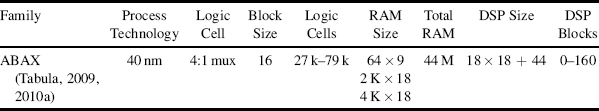
The rapid reconfiguration is achieved by having a stack of up to eight active configurations available. The user clock is multiplied up by the number of active configurations to give the internal system clock. Then with each internal system clock cycle the active configuration is cycled between those available. Thus each component is effectively being time-multiplexed up to eight times each user clock cycle.
At the time of writing, full data was not available on the internal components of the ABAX FPGA. The logic cell appears to be based on a 4:1 multiplexer, but may be more general than this. Four of these are grouped into a slice, with associated arithmetic logic. A logic block appears to consist of four slices, giving a total of 16 logic cells per tile. However, since each block is used for different functions up to eight times per user clock cycle, the effective logic densities are up to eight times the physical densities listed in Table 2.6. On the output of each logic cell is a number of flip-flops to enable communication between the different time slices.
On the FPGA, there are three different sizes of block memory. The small 64 × 9 blocks can be used either as a register file or as a 6-LUT. The medium sized dual-port block can be configured from 16 K × 2 to 2 K × 18. It also has built-in FIFO control, reducing the logic needed to implement FIFO buffers. The large size blocks are single port with aspect ratio from 36 K × 2 to 4 K × 18. Dividing the user clock cycle into up to eight internal time slices also means that a standard single-port memory can be accessed up to eight times every user clock cycle, effectively creating a multiport memory with a large number of ports. The DSP block performs a pre-addition, an 18 × 18 multiplication, followed by a 44 bit sum. Like the rest of the FPGA, it is capable of running at up to 1.6 GHz with the internal system clock.
A wide range of I/O standards is supported, including DDR and LVDS signalling. High speed serial links have built in SERDES logic, although the protocols must be managed with user logic.
Although the primary target market is DSP for wireless networking, the ABAX devices should also perform well in an image or video processing context.
2.4.7 Actel
Actel provides a range of low power FPGAs, making them ideally suited for embedded applications. There are three main families: the Axcelerator, the ProASIC3 and the IGLOO. Also included in Table 2.7 for comparison is the SmartFusion family, which includes an ARM processor and programmable analogue circuitry in addition to a ProASIC3 based FPGA block.
Table 2.7 Characteristics of the Actel FPGA families.
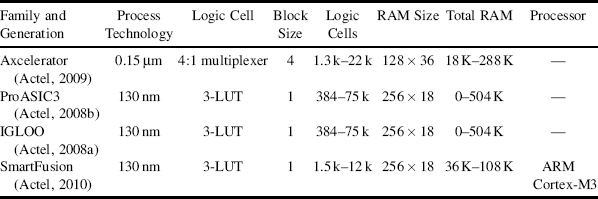
The Axcelerator family is one-time programmable using anti-fuse technology. Once programmed, it cannot be reprogrammed. A big advantage of one-time configuration is that it can begin operating immediately on power-on. The basic logic cell is a 4:1 multiplexer, which makes it different from the other cells looked at so far. Associated with each multiplexer is additional logic, including a carry chain, to make a full adder. A logic block consists of four such cells combined with two flip-flops. Although the logic is quite fine grained, it is relatively rich in memory resources, with a number of 4608-bit memory blocks. These memories are simple dual-port with configurable aspect ratio from 4 K × 1 to 128 × 36. The routing within the Axcelerator is relatively fast because the fuses do not introduce delay in the same way that pass transistors do. The lack of reprogrammability makes the Axcelerator best suited in embedded designs only where the functionality is not going to change.
The other families are based on flash memory programmed FPGAs. These also have the advantage that they are immediately ready on power-on, but with the ability to be reprogrammed if necessary. The basic logic element consists of a 3-LUT, which can also be configured as a D flip-flop. This makes them very fine grained and quite homogenous logically. Within the FPGA is a single block of 128 × 8 of user flash and a number of 4608-bit block RAMs. These can be configured from 4 K × 1 to 256 × 18 and are true dual-port within the ProASIC3 or simple dual-port within the IGLOO. The IGLOO also has hardware logic to use the RAMs as FIFO buffers. The larger devices are able to implement a 32-bit ARM processor as a soft-core block. While both families are low power, the IGLOO is designed particularly for ultra low power applications, making it ideal for embedded vision sensors. Both families are available in very small footprint packages (as small as 3 mm × 3 mm) making for an extremely compact design.
2.4.8 Atmel
The Atmel devices are relatively old technology, although they are still available. The main features are summarised in Table 2.8. The relatively small size of the FPGA (in terms of logic resources) limits what they can be used for in terms of image processing applications.
Table 2.8 Characteristics of the Atmel FPGA families.
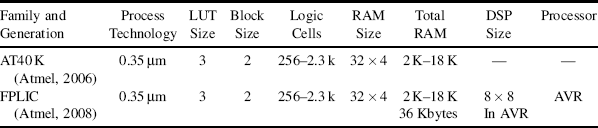
The logic cell consists of a 3-LUT, which are grouped two to a logic block. This enables a 4-LUT or full-adder to be implemented from each logic block. Each logic block also contains a single flip-flop. Small dual-port RAMs are distributed through the logic giving a relatively homogenous architecture. The devices are partially reconfigurable, enabling adaptive systems to be constructed where blocks of the design can be overwritten after the initial programming.
The FPLIC combines an AT40K FPGA with an 8-bit AVR microcontroller and 36 Kbytes of static RAM for the microcontroller instruction and data memory.
2.4.9 QuickLogic
QuickLogic used to make a range of FPGAs; its most recent family was the Eclipse (Table 2.9). Because of their age, the devices were relatively small, making them less suitable for many image processing applications. Their distinctive feature was that the logic was not LUT based, but consisted of a mixture of difference size AND gates and small multiplexers.
Table 2.9 Characteristics of the QuickLogic FPGA families.
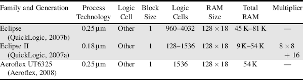
More recently, QuickLogic has moved from the FPGA market to providing much higher level application blocks that can be combined and customised for specific applications. A radiation tolerant version of the Eclipse is provided from Aeroflex that would be suitable for space-based applications.
2.4.10 MathStar
An alternative approach to programmable logic is taken by MathStar with its Arrix Field Programmable Object Array (MathStar, 2007). It is like an FPGA, but rather than the fine-grained logic blocks, it consists of a set of much coarser-grained building blocks. The advantage of this is that the coarse-grained blocks may be implemented more efficiently than building complex logic out of LUTs. However, unless the mix of blocks matches that required by an application, the resulting design may make poor use of the available resources. MathStar targets applications where there is significant mathematical computation (including image and signal processing) that can effectively make use of the coarser-grained blocks.
The Arrix is a 16-bit device in that all data paths are 16 bits wide rather than working with each bit individually as is the case with FPGAs. The available building blocks are:
- An arithmetic and logic unit (ALU). These have a 16-bit data path and can perform addition, subtraction and a wide range of logic functions. The ALUs are controlled by a reconfigurable state machine. The control bits which specify the operation come with the data.
- A multiply and accumulate block, that performs a 16 × 16 multiply, with a 40-bit accumulator.
- A register file that contains a 64 × 20 simple dual-port memory. The register file can also be configured as a 6-LUT (producing 20 outputs) or as a FIFO buffer.
- A block RAM. Each block is a single-port 2048 × 76 memory.
- An external RAM interface that facilitates connection to external DDR memories.
- A general I/O interface.
- A high-speed LVDS block with separate transmitters and receivers. These have built-in FIFO buffers to manage the flow of data onto and off the chip.
Two forms of interconnect are used: nearest neighbour and shared longer lines. The longer lines must be registered, giving them a latency of at least one clock cycle (longer for longer distances). Such pipelining enables a high clock speed to be maintained regardless of the length of interconnection. Each interconnect path is 21 bits wide: 16 bits for the data, one bit to indicate valid data and four control bits are used to control the ALU function.
While not strictly an FPGA, it is appropriate to use the Arrix for image processing applications.
2.4.11 Cypress
Cypress Semiconductor provides a series of three programmable system-on-chip systems. They combine an 8-bit, 16-bit or 32-bit microcontroller with a range of relatively high level analogue and digital building blocks or peripherals. Again, the blocks are too high level to classify them as FPGAs, and the underlying system is based primarily on the microcontroller rather than programmable logic. While these devices are less suited to real-time image processing applications, they may be appropriate when combining serial image processing (performed by the microcontroller) with a range of other sensors in a low cost sensor network.
Cypress Semiconductor also makes a wide range of peripherals (USB, wireless nodes, etc.) that provide a relatively simple way of integrating these functions within an FPGA system. Some of these are discussed in more detail in Chapter 7.
2.5 Choosing an FPGA or Development Board
Many FPGA manufacturers also sell development boards or evaluation boards. These boards often consist of an FPGA with a set of peripherals to demonstrate the capabilities of the device within a range of targeted applications. In particular, most boards provide some form of external memory and some means of interfacing with a host computer (even if it is just for the downloading of configuration files). Other than this, the specific set of peripherals can vary widely depending on the target application and market. Boards aimed for education use tend to be lower cost, often with a smaller FPGA and a wide range of peripherals, enabling them to be used for laboratory instruction.
With the large range of both FPGAs and development boards available, how does one choose the right system? Unfortunately, there is no easy answer to this, because the requirements vary widely depending on the target application, and whether or not a development system or product is being built.
For image processing, the development system should have the largest FPGA that can be afforded, with sufficient peripherals to enable a wide range of applications to be considered and programmed. Some essentials for any image processing application:
- There needs to be some method for getting images into the FPGA system. Depending on the intended input source, there are a number of possibilities here. To come from an analogue video camera, some form of codec is necessary to decode the composite video signal into its colour components and to digitise those components. Some systems provide a codec to digitise VGA signals, allowing the capture of images produced by another computer system. Common interface standards to connect to digital cameras include USB, Firewire and CameraLink. Most development boards have a USB interface (although actually getting to the video stream is more complex than just the physical interface), but few will have other camera inputs.
- The development board must have some method of displaying the results of image processing. While the final implementation may not require image display, it is essential to be able to see the output image while debugging. Either a VGA output or digital video interface (DVI) is suitable.
- The system must have sufficient memory to buffer one or more frames of video data. While the final application may not require a frame buffer, just capturing and displaying an image will require buffering the frame unless the camera and display are synchronised. Only the largest FPGAs have sufficient on-chip memory to buffer a whole image, and this memory is probably better used for other purposes in most applications. Therefore it is usually necessary for the frame buffer to be in off-chip memory. Dynamic memory has a variable latency, making it less suitable for high speed random access, although is suited for stream processing where the access pattern is known in advance. Static memory has faster access, although is generally available in smaller blocks. Working with two or more banks of static memory can often simplify an algorithm by increasing the memory bandwidth.
For systems where the FPGA is installed as a card within a standard PC, the host computer usually manages the image capture and display. The interface between the FPGA and host is usually through PCI express. Managing the interface with the host computer can use considerable resources on the FPGA. Depending on the application, the interface may also be a bandwidth bottleneck within the system.
When implementing a target embedded product, power and size are often the critical constraints. This will involve eliminating any peripherals that are unnecessary in the final application. However, for debugging it may be useful to have additional peripherals accessible through an expansion port. To minimise the cost of a product, it is desirable to reduce the size of the FPGA used. However, it is important to keep in mind upgrades that may require a larger FPGA. Many families have several different footprints for each size FPGA. Choosing a footprint that allows a larger FPGA to be substituted will reduce the retooling costs if a larger FPGA is required in later models.