
6.7 Two-Layer Boards
In conventional construction, a two-layer circuit board does not have a ground or power plane to form transmission lines. This means that a signal trace that interconnects components must have a nearby ground or power trace to form a controlled transmission line. For a logic and ground trace running in parallel on one surface, the characteristic impedance will usually be above 70 ohm. This results because the edge capacitance per unit length is a small value. There are several ways by which the capacitance can be increased to reduce the characteristic impedance, such as if the logic trace is placed between two ground/power traces, if the traces are thicker, or if the trace spacing is reduced.
The trace geometry we will consider for a two-layer board is a logic trace between two ground or power traces. The largest part of the field energy is concentrated in the space between the inner trace edges. We will consider trace widths and spacings of 10 mil.
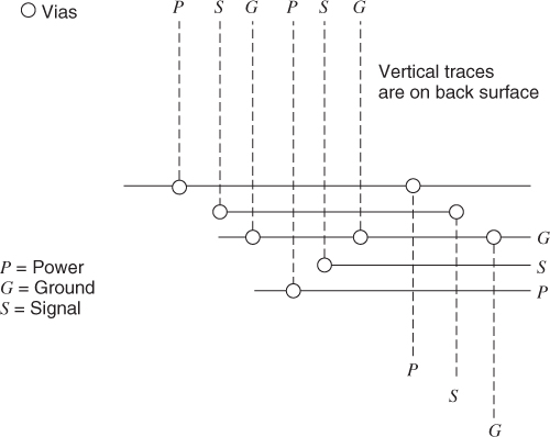
A possible construction for a fast double-sided board is to run traces left to right on the top surface and top to bottom on the reverse surface. The ground and power traces serve to connect power to the components and to form transmission line for each signal. It is good practice to use vias to interconnect ground and power traces on the two surfaces at regular intervals. These connections in effect form a pseudo ground/power plane for the board. Decoupling capacitors should be placed near the power and ground pins of each active component. Figure 6.13 shows a typical trace pattern.
Figure 6.13 Trace pattern for use on a two-sided circuit board.
The traces carrying power act as grounded traces as far as the characteristic impedance is concerned. When a logic signal propagates on the three conductors, the logic return current flows on both the power and ground traces. This means that the characteristic impedance is not a function of the static potentials on the traces.
The characteristic impedance Z0 of a logic trace between two grounded traces is given approximately by Equation 6.6:
where s is the spacing between traces, t is the trace thickness, and w is the trace width. The number of traces per linear inch is limited by the diameter of the via holes and the area of the surface pads that must be provided. Via hole diameters that are about 1/6th the board thickness are practical at little added cost. If the board thickness is 0.062 in then the hole diameter can be 10 mil. The pad diameter for a 10-mil hole is typically 25 mils, which means that trace spacing can be about 10 mil. If the board thickness is reduced then smaller diameter vias can be used.
For via pad diameters of 25 mil, trace spacing of 10 mil, trace widths of 10 mils, and a trace thickness is 2.7 mil, the characteristic impedance in air is approximately 73 ohm. If the traces are routed on a dielectric then half the field is in the dielectric. This means that about two-thirds of the transmitted energy is transported in the dielectric. The capacitance of the space in the dielectric is proportional to the relative dielectric constant. This means that if ε R is 4 then the characteristic impedance of traces in this space is half that of air. The characteristic impedance of three traces over a dielectric can be considered to be 2Z and Z in parallel or 2/3Z. In our example, this is an impedance of 48 ohm. If the trace thickness is 2 mil, the characteristic impedance is 50 ohm.
If the microstrip is coated with a thin dielectric, the traces need not be solder plated. This means that the surface currents will flow in copper that has a lower resistance than solder.
In board areas where there are no logic signals, ground and power traces can still be provided. An alternative is to flood these areas with copper and connect this copper to ground and power.
Vias are used to connect the logic traces in any required xy (Manhattan) pattern. The right angle bends in the transmission lines (signal path) will not introduce any significant reflections (Figure 6.14).
Figure 6.14 Treatment of the logic trace at a termination.

This connection geometry illustrates a basic problem in high speed logic. There is no way to reduce the loop area formed at the IC by the logic and ground connection. The pad and beam geometry forms a loop area that represents an uncontrolled section of transmission line. This loop area exists for all logic lines. Note that these loops are a source of radiation.3
Adding a ground pin next to every logic pin seems like a poor suggestion. The pin counts are quite high and rising. There still might be an answer if every pin is considered a two-conductor transmission line. Imagine a pin made of a stiff plastic strip with a plated conductor on each wide surface. One side would be logic and the other side would be ground. When the pin is installed in the board, the transmission line connection is automatically made.
If the traces carrying logic in the example mentioned above are separated by about 40 mil, there is the possibility of 25 traces per inch on each side of the board. For a 10 × 10 in board, that amounts to 500 traces running 10 in. If 30% of the board is taken by pads and 70% of the remaining board is useable, there can still be about 245 traces running 10 in. If the average trace run is 4 in, there can be 612 logic traces. If 70% of these trace runs are useable then the trace count drops to 428.
If a high trace count is not needed then the trace widths and spacings in the grid structure can be scaled up. Wider traces are in the direction to reduce both skin effect losses and cross coupling. A typical construction is shown in Figure 6.15. A typical signal termination is shown in Figure 6.14.
Figure 6.15 Via patterns for a logic transition.
