
6.9 Six-Layer Boards
Six-layer boards can be constructed by adding outer layers of copper foil to a four-layer layup. The layers of prepreg that bond the foil layers control the dielectric thickness. Another construction is to build the core from two clad laminates separated by prepreg and then add the outer layers of foil to form the layup.
A six-layer board allows for layups with adjacent ground and power planes. This geometry provides a distributed decoupling capacitor for the board. The closer the energy sources are to the loads the faster the energy can be supplied when there is a demand. The vias that connect this energy to the load must be closely spaced. This topic was covered in detail in Section 2.14.
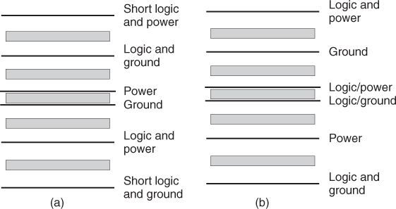
Trace layers must be near conducting planes for effective control of the characteristic impedance. It is preferred to have a ground or a power plane on each side of a trace layer. Examples of six-layer layups that can be a problem are shown in Figure 6.18.
Figure 6.18 Layup designs for six-layer boards that should be avoided.

In these layups, the ground/power planes are spaced, so they do not supply much energy to the logic. In Figure 6.18a, the outer logic layers are not near a ground or power planes so that cross talk is likely.
In logic designs where the rise and fall times are short, the problem of cross talk is present. In general, cross talk is reduced for traces that are between the conducting planes. For this reason, it is desirable to place shorter trace runs on outer layers and longer trace runs on inner layers between the conducting planes. In high speed circuits, it is desirable to use embedded microstrip for outer layers. This reduces the level of forward wave cross coupling. This point was covered in Section 3.11. Two recommended layups for six-layer boards are shown in Figure 6.19.
Figure 6.19 Acceptable layup designs for six-layer boards.
“Flooding” areas with copper to form ground or power planes is always recommended. A ground or power plane will reduce radiation or cross talk only where the plane forms a transmission line return path for traces. In other areas, it makes the board more robust and helps to radiate heat.
The flooded areas that are under (over) traces will affect the characteristic impedance of nearby traces. Placing conducting planes near a part of a trace run can create problems if the characteristic impedance varies along the trace run. Obviously, power planes and ground planes that are not closely spaced may not contribute much energy for use in decoupling the board.
Traces that transition between layers must receive special attention. The return current must also transition so that the characteristic impedance of the transition is controlled. It is important to realize that fields cannot cross through a conducting plane except where there is a hole. If the transition causes significant reflections then the result is a problem in signal integrity.