4.18 The Control of Connecting Spaces
Traces over and between ground planes define the spaces used by fields to propagate signal or energy. These spaces must be controlled along an entire path or there will be reflections resulting in delays. A good design controls the spaces between conductors and not just the geometry of the traces. This control must be for both signal propagation and the supply of energy from decoupling capacitors.
A problem can occur when the path of energy flow must transition between traces and components or between layers on a circuit board. The problem of connecting to a decoupling capacitor has already been discussed. The problem of connecting to the pins of a component can also be an issue. If the field must cross from the outer surface of a pin to the inner surface to reach the die then the field must spread out. This can be viewed as adding inductance or more properly as a change in characteristic impedance, which results in delays caused by reflections. A transition that is only 1/16th inch long can cause trouble when the rise times are very short.
A problem that is often ignored is the connections to a metal-cased power transistor. The only entry point for field energy is through the spaces around the pins. There is no way that field energy can transition through the metal enclosure. This includes energy to run the device and energy that leaves the device as signal.
The problem of supplying energy to a circuit from a low impedance source requires that the characteristic impedance be controlled along the entire energy path. To have low characteristic impedance, the spacing between conductors will usually be under 1 mil. This is true whether the path involves conducting planes, capacitors, DTLs, traces or coaxial cable. Controlling small dimensions at an interface poses a problem. This is a system problem as components must be compatible at the interface for both signal and power flow.
Interconnections where small spaces must be controlled requires compromises. Some misalignment must be permitted to make any connection at an interface practical. If the transition is limited to a few mils in length, the effect will not be noticed. Note that a length of 60 mils would be considered excessive. The example shown in Figure 4.7 shows a connection between a coaxial line and a component.
Figure 4.7 A coaxial connection to a component.
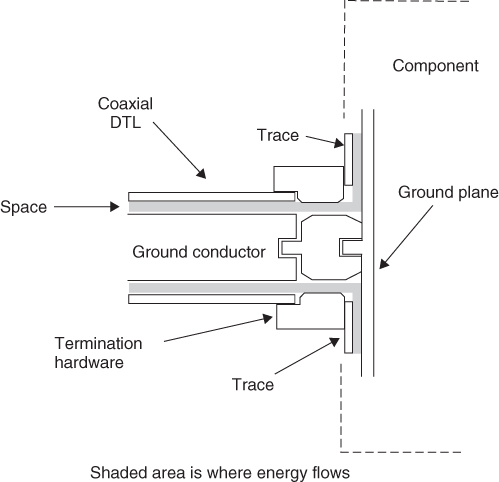
The edges of all connections must be chamfered to allow for misalignment. Note the way that the conductor geometry controls the space that is used by the fields.