3.5 Common Mode and Normal Mode
To appreciate the meaning of these terms, it is worth discussing the rejection of common-mode interference in analog circuits (below 100 kHz). The circuit geometry is very similar to the arrangements found in logic transport between different pieces of hardware. In analog signal processing, the signal of interest is often generated at a remote point and carried to conditioning electronics over a long cable. The zero or reference potential for the signal is often carried on a shield conductor G1 that is grounded near the signal source. The circuits that amplify the signal are associated with a second ground G2 located at the point of amplification.
The potential difference that can be measured between G1 and G2 at G2 is generated by fields in the area of cable routing. Consider a cable routed between two pieces of hardware. Fields in the area cross the loop formed by this cable and nearby conducting structures (grounds). These fields are often related to utility power, but they can include fields from radio and television transmitters, as well as digital circuitry. Signals that are observed between G1 and G2 at the receiving end of the cable will also appear between G1 and all the signal leads in the cable.4 This common signal must be attenuated or filtered so that the signal of interest (signal difference) can be amplified. This average or common signal is called a common-mode signal. For low frequency analog signals, these circuits are called differential amplifiers. This type of linear amplifier conditions (amplifies) the signal of interest (normal-mode signal) and attenuates the common-mode signals. In analog instrumentation, the common conductors are not usually connected together at the interface.
For signal conditioning above 100 kHz, the shield of a connecting cable should be grounded at both ends. This is the case when digital signals are transmitted over some distance. Consider Figure 3.2 where an external cable carries signals between devices.
Figure 3.2 A long cable between devices. Note: The shield may not be present.

Fields in the area will use the cable shield as one side of a transmission line. The return path can be racks, shields, other cables, or earth. The protection that could be provided by a close conductive plane is absent. This means that external fields can couple to the loop area formed by the cable and its return path. When this cable is connected to a circuit board, the arriving energy becomes a part of the general ambient. Some of the energy is reflected and some of it follows conductors and traces to their terminations on the circuit board. The average interference signal present on a group of logic lines, when measured with respect to a local common or ground, is called a common-mode signal. In digital parlance, this signal adds even-mode interference to odd-mode logic. This interference can use up available noise budget.
Definition: Common-Mode Signal. The average interfering signal on a group of conductors measured with respect to a local reference conductor.
Definition: Normal-Mode Signal. The signal difference of potential between a pair of conductors. A normal-mode signal is also called the signal of interest.
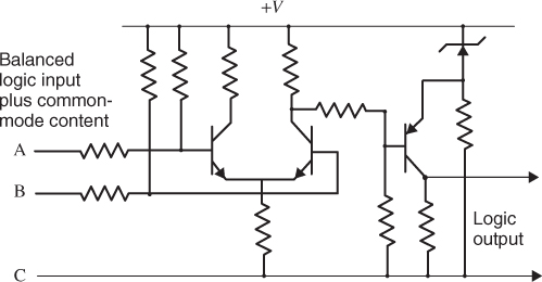
Cables often carry balanced logic lines through connector pins and then onto connecting traces. These traces may be stripline or microstrip. The receiving traces and their termination require careful attention. A typical common-mode rejection circuit is shown in Figure 3.3. Note that this circuit can accommodate interference that drives the input leads negative.
Figure 3.3 A differential logic circuit.
When a logic stream must cross between different pieces of hardware, external fields in the area will couple common-mode interference into the signal path. If the signal is balanced and if the cable pair is balanced, any coupled common-mode interference can be rejected by the electronics. A balanced signal pair means that the average signal is a constant. A balanced cable pair means that interference couples equally to both lines. A balanced logic signal requires that when line 1 is at a logic 1, line 2 is at logic 0 and vice versa. A balanced cable pair implies that an interfering field will add the same voltage to both logic lines. If the logic is 0 and 5 V, the interference at one moment might add a half volt to each line. At that moment, the logic signals are 0.5 and 5.5 V. The logic only considers the difference that is still just 5 V.
The termination of an external cable carrying a balanced signal requires some explanation. For short rise-time applications, the line termination should take place at the receiving logic. In many slower applications, the termination resistors can be located at the connector. Let us treat the short rise-time case first.
The balanced line impedance of a cable is typically 100 ohm. This impedance should be matched where the cable enters the board. If the cable connects to two 50-ohm traces then the two trace impedances appear in series, and this matches the cable impedance. These traces must not be closely spaced or the cable will be doubly terminated. In effect each trace as a transmission line carries half of the energy flowing in the cable. At the electronics, the two transmission paths are terminated in 50-ohm resistors (Fig. 3.4).
Figure 3.4 The termination of a balanced transmission line on a circuit board.

If the cable terminates on parallel board traces that form a 100-ohm transmission line, there are really three energy paths, namely, the path from each line to ground and the path between traces. Each path must be terminated or there will be reflections. If the ground plane is removed then there is only one energy path and one terminating resistor.
If the terminating resistors are placed at the cable connector, the traces from the connector to the IC form a stub. If this stub is shorter than one-quarter the distance a wave travels during the rise time then there will be no problem.
Cross talk has the effect of introducing jitter into logic. Ideally, if the common-mode interference affects each lead equally, the effect is balanced out and the logic transition time is not affected by the interference. Traces carrying balanced signals should not be routed parallel to long traces carrying unbalanced signals. If one of the traces should couple to interference this is odd mode coupling. This mode is not rejected in the electronics.