
Chapter 4. Cell and IP Modeling
4.1 Functional Modeling for Cells and IP
Functional models are written in a specific hardware description language (HDL), for which EDA vendors have developed corresponding simulation tools. The semantics of an HDL model consist of a set of concurrent sequential processes (CSPs). In short, a set of model processes (or procedures) are compiled. Each process has an input sensitivity list of signals; a transition on a signal in that list results in the execution of the statements in the process. Evaluation of the statements in the process/procedure proceeds sequentially to completion (or until a wait statement clause is encountered). All model processes are pending concurrently, and once active, they may execute in parallel (i.e., all starting at the same reference point in simulation time).
As described in the following sections, several levels of modeling abstraction are used to represent the logic functionality of an IP block and individual library cells using an HDL.
4.1.1 Behavioral Modeling
A behavioral model represents the (complex) functionality of a large IP block using programming language semantics typically associated with sequential statement execution. Procedures, processes, and functions are written using a combination of logical and arithmetic operators and statements that execute sequentially, following the CSP paradigm. The HDL sequential statements available for modeling include the control flow typically available with conventional programming languages, including if-then-else, (conditional and fixed iteration) loops, and case statements. As mentioned previously, the process is invoked when a change in value is assigned by the simulator to a signal in the input sensitivity list of the routine, as illustrated in Figure 4.1.
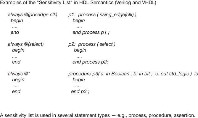
Figure 4.1 An HDL model consists of a set of concurrent, sequential processes. An example of a process and its sensitivity list are illustrated. Both Verilog and VHDL examples are depicted.
Although similar statement types are used, several aspects of the behavioral HDL model distinguish it from a conventional programming language, as discussed in the following sections.
Representation of Simulation Time
The statements used in behavioral HDL models reflect the times at which the results of statement evaluation are reflected by the simulator. As illustrated in Figure 4.2, a statement may have an additional clause that provides an explicit delay, which the simulator posts to a future event queue.
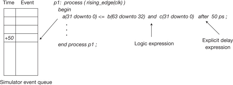
Figure 4.2 Illustration of an HDL statement with an explicit time delay until the assignment is to be applied to the simulation model. A pending update is posted on the event queue.
The HDL language semantics also include an immediate assignment statement. The result of this statement execution is an immediate assignment to the left-hand side variable, without advancing simulation time. Subsequent statements in a sequential procedure use the updated values, as illustrated in Figure 4.3.
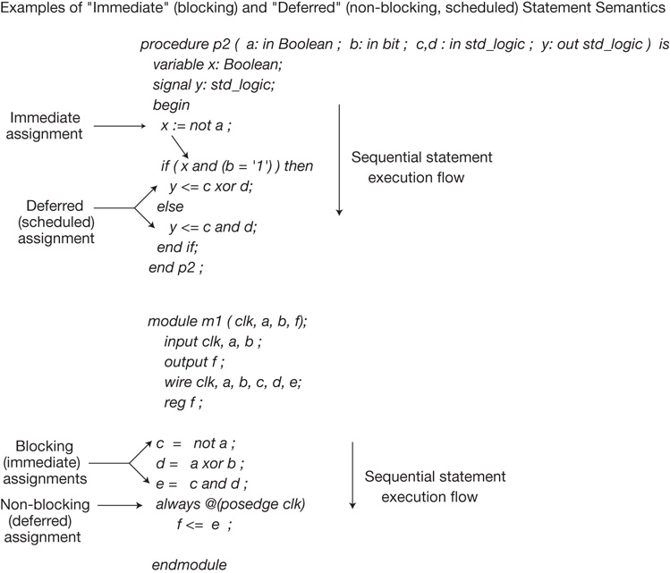
Figure 4.3 An immediate assignment statement executed in a CSP updates the left-hand variable value directly after evaluation of the right-hand side expression rather than posting to the event queue.
The representation of simulation time also includes the concept of an infinitesimal delta delay. An assignment of a new signal value from executing a deferred statement without a delay clause is not reflected immediately. Rather, the deferred assignment value is placed on the simulation event queue, to be evaluated at a delta time in the future, after all sequential statements in all active processes are complete. The explicit simulation time is not advanced until the delta event queue is empty and the next pending event explicitly advances the time base (using an “after n psec” clause). Figure 4.4 illustrates the evaluation flow.
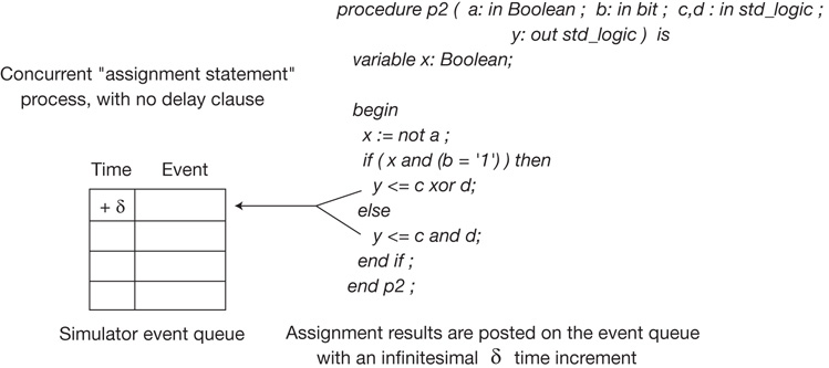
Figure 4.4 A non-immediate assignment without an explicit delay clause is posted to the event queue in an infinitesimal “delta delay” after the current simulation time. After all active processes complete, the event queue is evaluated, and new processes (and delta time assignments) are active. Simulation time does not explicitly advance until there are no pending events on the delta time queue.
Variables and Signals (VHDL), Wires, and Regs (Verilog)
The declaration of HDL model identifiers differentiates between the left-hand side targets of immediate (also known as blocking) and deferred (non-blocking) assignments. An immediate assignment is made to identifiers declared as variables (VHDL) or wires (Verilog). A deferred assignment is made to signals (VHDL) or regs (Verilog).
Resolution Function
In the specific case in which multiple assignments to the same signal from different statements are pulled from the event queue at the same (delta) time, a resolution function is invoked by the simulator to calculate the value to be assigned to the signal. The specific resolution function is associated with the type declaration of the signal (discussed shortly).
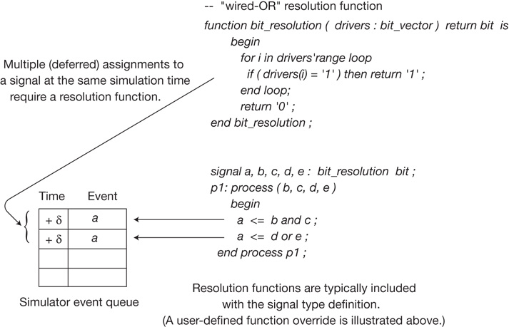
Figure 4.5 In the case in which multiple assignments to the same signal are present on the event queue at the same time (originating from one or more processes), the simulator evaluates the resolution function corresponding to the signal type to determine the assigned value. A “wired-OR” resolution function description in VHDL is shown.
Data Structures
A conventional programming language typically provides data structures that are based on collections of variables, such as vectors and multidimensional arrays, records, and linked lists with pointers (where variable values are references as address pointers to other variables). The HDL design model is typically presented to a behavioral synthesis flow; data structures that are “non-synthesizable” are not typically included in the model. Note that HDL testbench models compiled with the design model for functional simulation validation are typically able to utilize the breadth of HDL statements, including non-synthesizable constructs. A hardware simulation accelerator used in the validation methodology may restrict the testbench modeling style if all or part of the testbench stimulus and monitoring features are to be incorporated on the accelerator.
Types
Like programming languages, HDL behavioral models associate type declarations with each variable and signal. The compilation and elaboration of a simulation model check the validity of the right-hand expression as an appropriate result to assign to the type of the left-hand statement identifier. Typical HDL language types for logic signals define the enumeration of discrete values that are valid assignments for Boolean operators—for example, ‘1’, ‘0’, ‘U’ (uninitialized), ‘Z’ (high-impedance), ‘D’ (don’t-care), and ‘X’ (undefined, typically due to an error condition detected within the model). Other levels of modeling abstraction may utilize additional type values, as discussed shortly.
At the start of simulation time t = 0_minus, the type’s default (or initialization) value is assigned by the simulator to signals and propagated throughout the model to reach an appropriate initial state. Subsequently, the simulator advances to t = 0, where the testcase stimulus is applied. An uninitialized signal present in the simulation model well after t = 0 identifies logic paths that may not have adequately propagated the desired initial (or reset) condition. To expedite simulation runtime, a specific model state can also be provided to the simulator to avoid having each testcase exercise an initialization preamble.
The type definition also includes the resolution function to be evaluated when multiple assignments to a signal are active at the same simulation time.
Each type definition can typically be expanded to allow vectors and arrays (vectors of vectors) to be easily defined. The indices to these structures are typically integers, and the definition would support ascending or descending index ranges.
A behavioral model commonly utilizes additional types beyond Boolean logic definitions. For improved simulation execution throughput and coding productivity, the behavioral model is likely to also include integer, floating point, and enumerated types, the latter being especially advantageous for describing machine state. The integer and floating point types have corresponding arithmetic and relational operators in HDL semantics.
For the synthesis of the behavioral model to a detailed hardware description, the integer type declaration for a signal needs to be bounded when the identifier is declared. The valid bounds ultimately define the number of bits required to represent the identifier in the synthesized implementation. These bounds are also used in the simulator’s real-time range checking. The IEEE-754 standard provides the definition for 32-bit and 64-bit floating point value representation (and arithmetic evaluation) for behavioral synthesis.
Inferred State
The sequential statement execution within an HDL process may result in a signal that is not necessarily assigned in each sensitized execution of the process. The example in Figure 4.6 depicts an if-then-else conditional statement in which the set of assigned signals differs in the potential statement execution paths. If a signal present on the left-hand side of an assignment statement is not explicitly updated during process execution, the current value of the signal is retained in simulation.
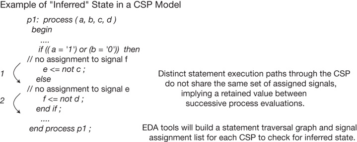
Figure 4.6 A signal that is not assigned during the execution of a CSP implies that the signal value is retained (i.e., an inferred state).
As a result, when synthesizing the behavioral model to a logic network, the value of the signal needs to be retained between evaluations of the process: An inferred state is implied. The resulting synthesized netlist includes a register, clocked by any of the input sensitivity list of the process, retaining its current value when the synthesized logic bypasses a new assignment to the signal.
Note that a loop construct in the behavioral HDL code denotes an explicit state machine.
Modules/Entities and Configurations
The HDL behavioral model also differs from a programming language with the additional support for a logical hierarchy. The model functionality is allocated to hierarchical elements denoted as modules (Verilog) or entities (VHDL), as illustrated in Figure 4.7.
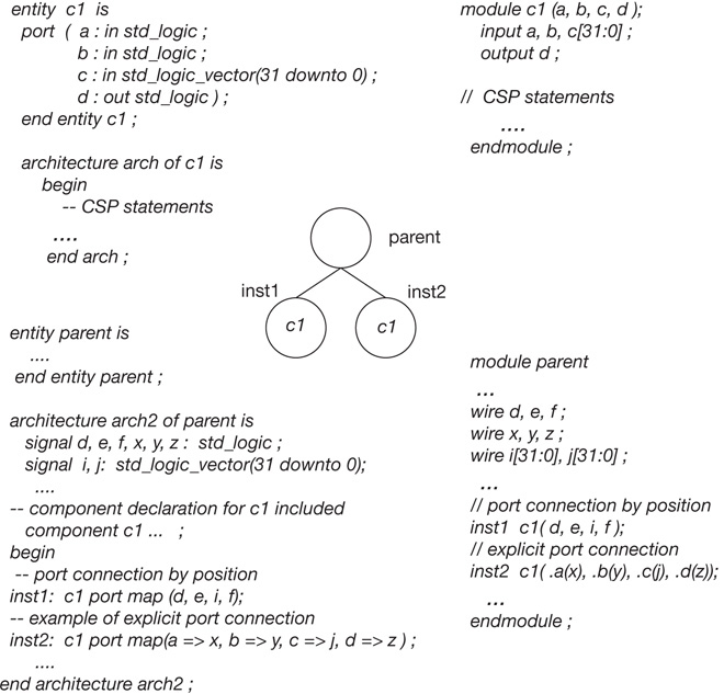
Figure 4.7 A hierarchical model is constructed using the definition of an entity (VHDL) or a module (Verilog) and then adding a component instance in the parent model.
Using VHDL semantics as an example, the connectivity to an instance in the logical hierarchy is through the ports of the entity. Signals defined in the parent connect to the ports of the child entity instances within the body of the parent model. During model compilation and elaboration, the signal-to-port connectivity is verified to ensure consistency of type and range declarations.
To provide increased flexibility in modeling styles, compilation may utilize a configuration specification (not to be confused with the DDM configspec described in Section 2.5, although they are similar in concept). This specification identifies a specific body that is to be associated with the entity/module definition when compiling the model. In this manner, different body code can easily be inserted, maintaining the same (invariant) connectivity throughout the logical hierarchy. For example, an RTL- or netlist-level model could replace a behavioral model at a subsequent project phase of functional validation by modifying the configuration specification. This model build approach simplifies the task of aligning the simulator used for each validation phase with the optimal model coding style.
Scope
The CSP execution paradigm includes the definition of the scope of an identifier, similar to a general programming language. A declaration of a local identifier implies that the value is not visible outside the process; it cannot be referenced by other (concurrent) processes. This enables independent HDL model development between blocks, as well as the integration of external IP models, without concern for identifier collisions. The EDA vendor simulator tool is likely to offer features that bypass the scoping rules of the HDL standard; for example, internal values in a process are visible to query during interactive simulation, breakpoints could be set to pause execution upon an internal value condition, and so on. In these cases, the simulator uses the hierarchically qualified instance prefix to access an internal identifier.
The behavioral abstraction typically simulates efficiently, with model compilation leveraging many of the optimizations developed for software programming languages. This style is commonly used by hard IP providers. Complex memory array and processor core IP are more readily modeled using the full HDL language semantics. Behavioral modeling is emerging as an attractive abstraction level for design IP, as well, especially for signal processing applications that perform arithmetic manipulations on streaming data packets. The numeric data types, arithmetic operators, and loop statements enable concise model coding and, thus, reduce the likelihood of design bugs. EDA vendors have also contributed to the growing adoption of behavioral modeling, with support for an increasing set of high-level HDL semantics in their behavioral synthesis tools.
4.1.2 RTL Modeling
The most prevalent HDL modeling style in SoC design uses an abstraction denoted as register-transfer level (RTL). All storage elements are explicitly coded; thus, all registers are readily identifiable in the HDL source code, as illustrated in Figure 4.8.
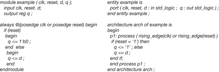
Figure 4.8 The register-transfer level (RTL) coding style incorporates explicit register assignment process statements, where the sensitivity list consists of a clock signal.
An RTL model of a design block includes a smaller set of HDL statement semantics than a behavioral model. No inferred state through the execution of conditional statements in a CSP is allowed (i.e., all branches through the clauses in if-then-else and case statements require assignments to a complete and consistent set of signals). A common coding style is to express combinational logic as stand-alone CSP statements (see Figure 4.9); the signals on the right-hand side become the sensitivity list for statement execution.
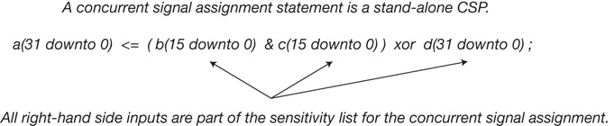
Figure 4.9 A concurrent, deferred assignment statement is equivalent to a CSP. The right-hand-side expression inputs are the elements of the sensitivity list. VHDL semantics are shown in the figure. Verilog uses a different method, with combinational logic represented by immediate assignments and coded outside the always statement.
The RTL coding style typically uses a limited set of signal types. The EDA industry has established de facto standards for type declarations, supported signal values, and operator evaluation for these types.
Simulation of an RTL model proceeds by calculating the combinational logic values to “transfer” to register signals each successive clock cycle. The RTL statements rarely include detailed delay information associated with any expression; the simulation timebase is advanced by the periodic clock signal input stimulus from the testcase. The RTL style enables simulation optimization during compilation. A cycle simulation tool assumes that only register signal values need to be recorded each cycle, in an output trace file for subsequent debug. Combinational signal values are not recorded (under the assumption that their values can be recalculated during debug from register values). The compilation of the cycle simulation model levelizes the RTL assignment statements between registers—no combinational loops are allowed—and optimizes the resulting compiled code. (Note that the cycle-optimized simulation execution requires special consideration for design blocks on different clock domains to achieve fastest simulator performance.)
Logic synthesis support for RTL model abstraction has been an established toolset from EDA vendors for decades. The synthesis flow identifies the registers in the design, constructs the combinational networks, and exercises optimization algorithms prior to technology mapping (e.g., constant value propagation, redundant logic removal, common sub-expression factoring). And, as mentioned previously, the RTL synthesis flow initially confirms that combinational network loops and statement clauses with inferred state are not present in the model.
As with behavioral coding, RTL models include a structural hierarchy of modules/entities. An SoC typically includes a mix of behavioral models for hard IP instances and RTL for design blocks.
Power domain information for the SoC design is typically not represented in either the behavioral or RTL model descriptions. The specific implementation of domain power gating (and internal state retention) for a sleep state operating mode is captured in the separate power format description rather than the RTL model. During RTL synthesis, consistency checks are evaluated to ensure that the power format description aligns with the RTL model.
4.1.3 Netlist
The most detailed HDL model representation is a netlist, consisting solely of structural instances of elemental cells from a library. No assignment statements are present. The netlist model could be generated by the logic synthesis flow or translated from a graphical schematic consisting of library cells, as depicted in Figure 4.10. The detailed text data in a netlist are rarely keyed in directly.
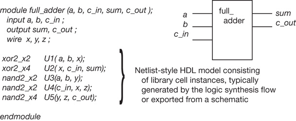
Figure 4.10 A netlist-style description is generated by the logic synthesis flow consisting of library cell instances. A netlist could also be exported from a schematic entry tool that uses graphic symbols for library cells. (A custom macro circuit-level netlist would be exported from device-level schematics.)
The use of schematics to represent a netlist may reflect the desire to build a block (or sub-block) from the bottom up, where the critical performance of a digital (or mixed-signal) function necessitates technology-specific cell selection and early timing simulation rather than using logic synthesis driven by timing constraints. Due to the rather poor simulation performance of a detailed netlist model, an RTL model for the schematic function is typically developed as well. The schematic-based netlist is subsequently presented to the logic equivalency checking (LEC) flow against the RTL model.
Note that the technology-specific netlist contains cell instances that do not add to the logic functionality of the model (e.g., parallel/serial repowering trees for high-fan-out signals). The netlist also includes the cells inserted to match the power format specifications.
4.1.4 Additional Functional Model Considerations
Regardless of the language description style used for each node of the logic model hierarchy, there are additional considerations for successful simulation:
Initialization—An HDL signal type has a default initial value. In addition, HDL statement semantics allow an overriding initial value to be coded in the model, as illustrated in Figure 4.11.
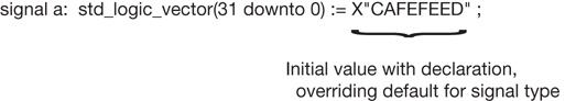
Figure 4.11 Initialization values in the HDL model override the default init value for the signal type.
To simplify coding and improve testbench efficiency, EDA simulators support the use of an external initialization file to establish the time t = 0_minus values on (a subset of) signals in the design. Note that these values are logically propagated at t = 0 in delta time. The simulation methodology flow needs to support use of an external init file, the capture of init state from a separate testcase that performs model reset(s), and a check to confirm consistency of the init file with the reset testcase results.
Test model views—The netlist model is used for test pattern generation. For logic primitive cell instances, the HDL representation of the cell is used directly by the EDA test pattern generation and fault simulation tools. However, for more complex cells, the functional description could be expanded to better reflect the circuit-level faults that contribute to the test pattern coverage measures. Figure 4.12 shows an example of a netlist instance in which the cell model could include two HDL views: one for simulation/equivalency flows and one for test analysis. The methodology team works with the cell library modeling and test teams to define how these alternative views are presented to the model compilation step of different flows.
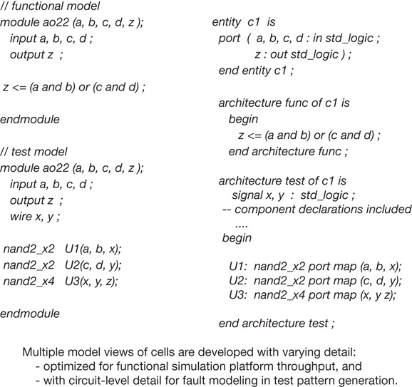
Figure 4.12 A cell (or IP block) could utilize multiple netlist views for different flows. A simulation view and a test view are illustrated.
The netlist also includes the full structural detail of the DFT architecture on the SoC (e.g., serial scan chain connectivity, test clocking).
X- and don’t-care modeling—The behavioral and RTL models are likely to utilize don’t-care designations when writing vector-based comparisons in conditional expressions, as illustrated in Figure 4.13. The use of the don’t-care designation makes the model coding easier and more readable; simulation compilation and logic synthesis disregard these bit comparisons.
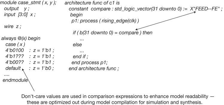
Figure 4.13 Don’t-care values are commonly used in HDL comparison expressions to improve code readability.
An additional model value designation—commonly, an ‘X’—is used to indicate that an erroneous condition has occurred, as part of a behavioral, RTL, or netlist model. For example, if an attempt is made to concurrently write to the same address from multiple write ports on a register file, an invalid value should be recorded (see Figure 4.14).
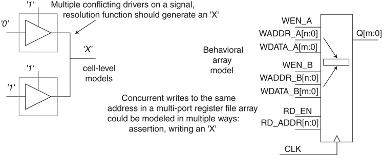
Figure 4.14 An unknown or undefined ‘X’ value may be assigned to a signal to represent an anomalous condition during simulation.
The propagation of an ‘X’ value on a signal in simulation usually expands throughout the network and can readily be detected. However, the evaluation of HDL statements with an input error value may provide unexpected results, as the behavioral or RTL model may not be coded to respond to unexpected conditions, as shown in Figure 4.15.
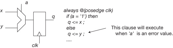
Figure 4.15 HDL models may not expect an ‘X’ value to be present at statement inputs and thus might not propagate the (internal) error condition. A methodology review of ‘X’ generation and propagation coding styles is needed to ensure consistency throughout the model.
If the ‘X’ signal value is to be regarded as an unknown value, rather than as indicating an error condition, a different simulation algorithm may be invoked. To enable testcase evaluation to continue, EDA simulation tools have implemented algorithms to set the ‘X’ signal value to both ‘1’ and ‘0’, evaluate the model twice, and merge the results. The methodology and functional validation teams review the modeling conditions that generate an ‘X’ value and determine what simulation tools settings are appropriate.[1,2]
Rather than rely on X signal value propagation, a more precise approach to handling model error conditions during simulation would be to add functional assertion statements to the model. In general, an assertion statement defines an invariant “true” expression and can be regarded as another concurrent process during simulation execution. (Sequential assertions embedded within a CSP are also available and would be evaluated only during sequential statement execution in the process.) Figure 4.16 shows an example of an assertion statement that includes an additional severity parameter.
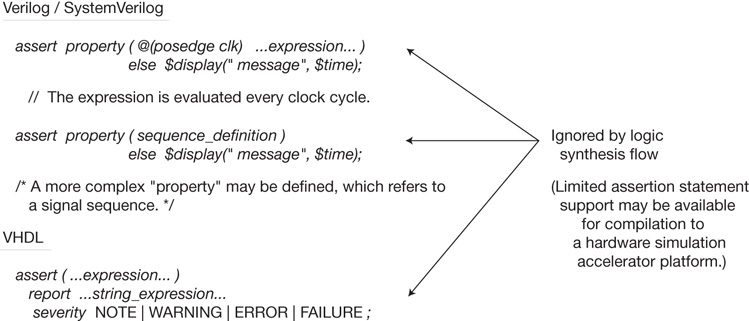
Figure 4.16 An example of an assertion statement to continuously monitor the simulation model for a specific condition. A severity clause is included, and it can be used to control how simulation proceeds if the assertion condition becomes false.
The EDA simulation tool includes settings that define what execution steps to take when as assertion statement of a specific severity is fired (i.e., when the “always true” assertion evaluates to false). An example of this simulation setting would be “stop_on_ERROR, continue_on_WARNING.” Rather than rely on the evaluation and propagation of ‘X’ signal values during the testcase, assertion-based validation enables more precise detection of anomalous simulation behavior. Both the simulation control setting and assertion output messages enable improved debugging. Further, EDA vendors now provide tools to analyze the model functionality to formally prove whether an assertion is always valid, without depending on functional simulation; if the assertion could be invalidated, the tool provides simulation counter-examples that fire the expression.
An assertion is a non-functional statement in an RTL or behavioral model. Assertions are skipped by logic synthesis tools when generating netlists. There is one exception: The synthesis of a model for a hardware simulation accelerator may be able to compile simple assertions into equivalent accelerator primitives with an output error signal, thus including the intent of the assertion in the accelerated simulation execution.
4.2 Physical Models for Library Cells
The physical model for each cell is based on the abstract view. The abstract defines the cell area and pin locations. Typically, the cell abstract includes power/ground pin definitions, as well, for coverage by the power and ground grids in the block physical design once the cells are placed. (It is uncommon for cells to include grid segments within the cell layout.) In addition to the abstract view, additional physical cell properties are required for subsequent flows:
Equivalent pin groups—Routing algorithms include features to deviate from the as-provided netlist, swapping signal connections among the input pins in an equivalent group to alleviate congestion.
Cell orientation options—Current fabrication processes require that all devices adhere to a single (vertical) orientation. As a result, the valid cell placement orientations are limited to mirror and flip operations. In addition, I/O cells have a strict distinction between left/right and top/bottom chip edge legal placements. The introduction of multipatterning decomposition among metal interconnect layers implies new placement orientation restrictions, such that the cell pin is consistent with the corresponding interconnect wiring track color, as illustrated in Figure 4.17.
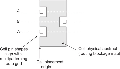
Figure 4.17 The physical locations of cell pins align with the multipatterning track color assignment for advanced process nodes.
4.3 Library Cell Models for Analysis Flows
4.3.1 Cell Models for Synthesis and Testability Analysis
The netlist model of an IP block on an SoC includes instances of library cells. The functional HDL model for each library cell may provide different views specifically developed for different flows. The library release includes information with each cell HDL model that enables the logic synthesis flow to select the correct functionality during technology mapping of the post-optimization RTL model. Specifically, the models for sequential cells (e.g., flops, latches) require a specific representation to be selected by synthesis, as these cells may have multiple clock/data ports, various (synchronous or asynchronous) set/reset input conditions, etc.
The testability fault model for the cell needs to be consistent with both the EDA tool capabilities and the prevalent manufacturing defect mechanism information from the foundry. Figure 4.12 provides an example in which the HDL model and Boolean gate-level model for a complex cell necessitate release of different views. Traditionally, test tools have utilized stuck-at pin faults on the gate-level cell model (i.e., test patterns are derived to generate and propagate values to demonstrate gate pins were not s-a-1 or s-a-0). This approach sufficed to cover the primary manufacturing defects, commonly localized to transistor operation. Note that CMOS logic circuits use complementary nFET and pFET transistors for each logic gate pin; the pin stuck-at fault model proved to be sufficient for early CMOS process technologies, merging the defect mechanisms of the two device types. More recently, resistive defects in the fabrication of contacts, vias, and local metal interconnects have led to the use of cell test models that may include greater detail. Test pattern generation tools may also accept a table of user-defined test pattern sequences for the cell that augment pin faults to exercise specific connections in the cell physical layout.
4.3.2 Cell Delay Models for Static Timing Analysis
Initially, cell delay models consisted of tables corresponding to input pin-to-output pin arcs. Each delay value in the table for each arc was a function of input pin slew and output pin (effective) capacitance load. Static timing tools would interpolate between these table entries to calculate the arc delay for each instance and flag cases where the network parasitics required extrapolation beyond the min/max slew and min/max load index values. Characterization of library cells would fill in these tables with measures from many circuit simulations, incorporating extracted circuit layout parasitics in the simulation model for each cell. Tables were provided for rising and falling input transitions for each pin. (Arc delay measurements are typically made between the 50% signal crossings of input pin and output pin waveforms.) The methodology team would trade off the number of table entries and the slew/load index range with the corresponding characterization effort for the library. Sequential cells required additional simulations for setup and hold time tables. Output pin waveform slew tables were also generated by the characterization flow, over the same input slew and output load index ranges as used to calculate the cell delay arc. The output pin slew for each cell delay arc was then used as part of the interconnect delay calculation, from the cell output to fan-out pins in static timing analysis.
The requirement for additional cell delay accuracy has recently led to the adoption of timing model formats that represent much greater detail and cell complexity. Pin-to-pin delay arcs may be conditional upon the logical values at other input pins, known as a state-dependent timing arc. The output signal slew table information proved to be inadequate for both interconnect delay calculation and the noise analysis flow. Current cell models replace each output slew table entry with a detailed (voltage or current) waveform representation. Interconnect delay calculation uses this waveform to determine the signal arrival and slew measures at fan-out pins.
Cell timing models are provided by the characterization flow for specific process tolerances, the supply and ground voltages (at the cell), and the (local) temperature values. The process tolerances span variations in fundamental device parameters, as well as a range of local interconnect dimensions after fabrication. The cell models are represented by a number of distinct parasitic extraction settings, each producing a unique netlist of resistance and capacitance elements between devices. Each extraction setting is selected to produce a netlist that biases the element values, such as max_R, max_C_total, max_RC, and max_C_coupling. The contribution of coupling capacitance is further complicated by the assignment of adjacent wires to multipatterning colors, with additional coupling variation due to the mask overlay tolerances.
The fabrication process parameters needed for characterization circuit simulations at each PVT corner require collaboration with the foundry engineering team. To maximize production yield, a set of worst-case (WC) process parameters is normally used for timing setup tests, while a best-case (BC) process would be used for hold tests. However, the definition of WC circuit simulation transistor and interconnect process values for circuit delay is not straightforward; setting all parameters to their statistical extremes from the foundry manufacturing measurement data requires establishing very conservative design performance targets. Rather, a set of WC characterization parameters is selected to represent n-sigma performance (e.g., 3-sigma performance from nominal). A set of representative circuit simulations is run, using sampled values from device and interconnect parameter statistical distributions. The resulting distribution of simulation measurements is analyzed to set an n-sigma process parameter sample that can be used across the library characterization flow.
The selection of the n-sigma parameters for library characterization assumes that the sampled delay distribution is Gaussian. The statistical delay for a representative library cell may have a different distribution shape, especially at low VDD supply values. As a result, the n-sigma performance target may need additional statistical analysis when selecting the characterization parameters.
Several simplifying assumptions are made when providing the n-sigma WC/BC cell delay model, for each operating voltage and temperature condition. The characterization values are used for all instances of all cells in the SoC netlist; the actual devices have some fabrication variation across each SoC die. A static timing analysis flow may introduce a unique margin for logic path and clock path cell delays to reflect the on-chip variation (OCV) when performing WC/BC setup and hold timing endpoint tests. (Section 11.4 discusses the use of derating factors in delay calculations.)
The use of n-sigma cell delay corner models is generally accepted for logic path timing analysis but may not be applicable to other IP blocks. For example, an array may incorporate such a large number of devices that a single n-sigma characterization approach cannot adequately represent the statistical variation within the array. A single device outside the WC process parameter set may result in an array weak bit that would be a significant yield detractor. (A single outlier device in a logic cell essentially results in a WC/BC delay anomaly that is only one constituent of a total path; its impact is less than an outlier present in an array, where no path averaging applies.) The array characterization must therefore be done to a high-sigma statistical process parameter set. The brute-force approach would be to run a large number of sampled Monte Carlo simulations on the array netlist, which would be computationally expensive. EDA vendors have developed unique “importance sampling” algorithms to reduce the number of simulations required to confirm high-sigma array behavior with high confidence levels.
Application-specific markets may also require high-sigma logic cell characterization, where the performance path averaging is not regarded as an acceptable trade-off, and there must be a high statistical confidence level in the calculated timing path delays.
Note that the cell delay model characterization reflects a single input transient, from which the pin-to-pin arc delay is measured; all other input values are assumed to be static. As illustrated in Figure 4.18, a multiple-input switching (MIS) event affects the actual circuit response.
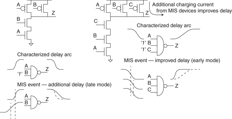
Figure 4.18 Example of a multiple-input switching (MIS) event at the cell inputs. Cell delay arc characterization currently assumes static values on other input pins. Both late-mode and early-mode arrival time propagation due to the multiple-input switching arrivals are depicted.
The static timing analysis (STA) algorithm adds path delays to calculate an arrival time and slew at each input pin. In Figure 4.18, for late-mode timing analysis, the arrival at input pin B occurs before the arrival at input pin A; although B is still transitioning when A arrives, the STA algorithm uses the A-to-Z delay arc to propagate the Z-falling arrival time, characterized with B at a static value. Thus, there is a degree of optimism in using the characterization delay to calculate the output arrival.[3,4] Conversely, for early mode timing analysis, multiple input transitions arriving shortly after the initial arrival could accelerate the delay transition; the arc characterization delay measured with static side inputs would be optimistic for hold time. The methodology team needs to review what MIS-based cell delay calculation derating features are provided by the EDA tool and to what extent those features should be applied in the static timing analysis flow to “margin” path delay calculations.
4.3.3 Power Analysis Characterization
Cell model characterization data is required for calculation of SoC power dissipation. There are three contributors to power dissipation associated with an individual cell (see Figure 4.19):
A switching transient on the output capacitive load
The cross-over current during a switching event, as the complementary devices in a CMOS circuit transition from active to off
Static (sub-threshold) leakage current
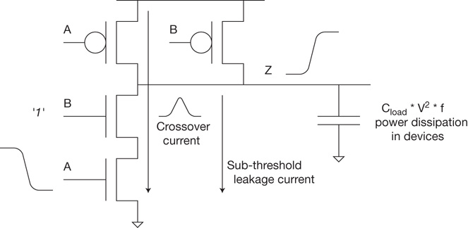
Figure 4.19 Contributions to cell power dissipation: subthreshold leakage current, cross-over current during a switching transition, and dissipation due to charging/discharging the capacitive load through the pullup and pulldown networks, equal to Cload*(V**2)*f, where f is the activity factor.
The power dissipation as a result of charging and discharging the output capacitive load is equal to:
where f is the frequency of the output signal transitions—the signal activity factor, in simulation terminology. The dissipated energy due to the cross-over current is a strong function of the input pin slew and can be measured during characterization. The sub-threshold leakage current is also easily determined, although specific characterization simulations are required. (For simulation efficiency, sub-threshold device current calculations are normally disabled during delay characterization.)
In addition to the data for cell power dissipation, the cell power model includes similar information used for the I*R voltage drop analysis flow for the power and ground distribution grids. A simplifying assumption is typically made for I*R analysis modeling. During a switching event, the saturated device current value is used for the duration of the transient, injected into the grid at the cell location, as depicted in Figure 4.20.
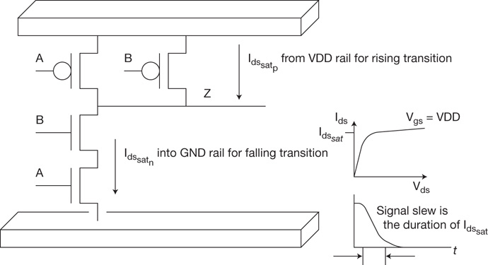
Figure 4.20 Power rail I*R voltage drop analysis requires modeling of the cell as a current source connected to the power rail for a switching transient.
The cross-over current in the other supply rail is typically neglected for the switching event. The cross-over current is indeed included in the cell power dissipation calculation, but its magnitude and duration would not contribute significantly to the dynamic I*R voltage drop in the other rail.
4.3.4 Cell Input Pin Noise Sensitivity
The noise analysis flow ensures that a capacitive-coupled transient from an aggressor does not result in an erroneous response on the circuitry associated with a victim signal and its fan-out cells, as depicted in Figure 4.21. The figure illustrates a “low-up” transient, representing the victim signal original value and the direction of the aggressor capacitive coupling. The driving cell will ultimately restore the signal to the correct logic value. However, the transient injected on the net will propagate at the fan-out cells, potentially resulting in an invalid network state.
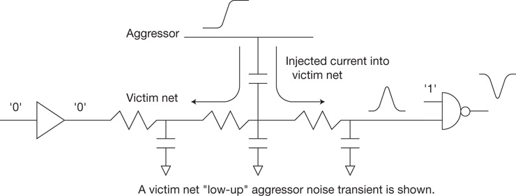
Figure 4.21 Model for a noise coupling event, from aggressors to a victim net.
The noise characterization of the library cell input pin determines the output transient due to an input noise pulse. The noise analysis flow determines how the coupled energy from the aggressor is dissipated through the victim net RC network and the pulse arriving at each cell input pin on the net. This input pulse at each victim net fan-out pin results in a perturbation at the output pin of the fan-out cell, to be further propagated by the noise analysis flow.
The characterization of the cell for input pin noise response requires specific features:
The interconnect extraction corner for characterization should maximize C_coupling.
The other (static) cell input values during characterization should be selected to maximize the gain of the input pin devices for maximum signal swing.
A set of magnitude/duration noise responses is required for each input pin (e.g., high_down, low_up). For circuit reliability, the characterization methodology should also establish high_up and low_down magnitude and duration data.
Figure 4.22 illustrates a simple input pin magnitude and duration curve from characterization (for a specific cell output load).
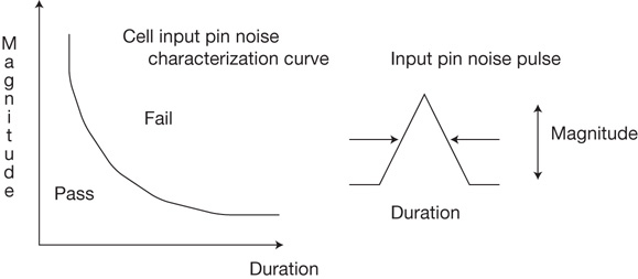
Figure 4.22 Cell noise characterization data. A simple pass/fail noise rejection curve is depicted. Characterization simulations sweep the input pin magnitude and duration for a range of output capacitive loads. The pass/fail delineation is based on an interpretation of the cell output response during characterization. At advanced process nodes, the actual noise pulse at the cell output pin is recorded for each simulation for the noise analysis flow to propagate this pulse through the network.
At advanced process nodes, the relative contribution of the coupling capacitance to the total interconnect capacitance on a net has increased. To maintain a suitable sheet resistivity with the scaling of line width, the aspect ratio of metal wires has been increasing in successive process nodes. As a result, the adjacent wire coupling capacitance is a greater percentage of the total wire capacitance. The graph in Figure 4.22 depicts a simple pass/fail curve from characterization for an input pin noise pulse. With this method, the noise analysis algorithm evaluates the arriving input pin pulse from a noise coupling event on a net and makes a direct pass/fail interpretation against the characterization noise curve. As discussed in Chapter 12, “Noise Analysis,” this restrictive pass/fail method is no longer suitable at advanced nodes, with the increased contribution of noise coupling from aggressors. Instead, cell input pin characterization exercises a simulation sweep of the input transient pulse magnitude and duration over a range of output loads and records the noise pulse measured at the cell output. The noise analysis flow now calculates the arriving noise transient at the input pin and subsequently propagates the characterization noise pulse from the cell output pin through the network. Additional aggressor events add to the noise pulses in the network simulation. The noise analysis flow determines the magnitude, duration, and arrival time of a noise pulse at a flop input to determine the risk of a network state upset error.
4.3.5 Modeling for Clock Buffers and Sequential Cells
A specific subset of the library cells is used in the distribution of clock signals. These cells consist of a limited number of logic functions, such as, inverters, buffers, and clock gating functions (refer to Figure 1.36). Characterization of these cells is slightly different than for the remainder of the logic library. Ideally, the rising and falling clock-to-output pin arc delays (RDLY, FDLY) at each corner should be equal, over the range of characterization loads and slews, to minimize clock phase jitter. The characterization range for clock-related cells may be more limited than for general cells; each drive strength option for these cells is typically designed for a rather precise load.
The noise characterization of these clock cells also involves more stringent magnitude/duration input pin limits, as the allowable output pin transient pulse is extremely limited. The fan-out set of these cells are other clock distribution circuits and sequential cell clock pin inputs, associated with very high-gain devices.
The characterization of sequential cells includes additional modeling requirements:
Setup and hold constraints apply at each corner. The measurement of setup and hold requires a number of circuit simulations, sweeping the arrival of the data input transition relative to the clock arrival, over the allowable slew range of each of these two input pins. The characterization flow team needs to collaborate with the library engineering team to determine what circuit simulation node measurements are appropriate to establish robust operation and what (maximum) deviations in those nodes are allowable when selecting setup/hold constraints (see Figure 4.23).
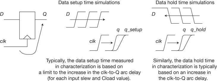
Figure 4.23 Sequential circuit setup and hold characterization measurements in circuit simulation.
The most direct setup and hold measurement criteria relate to the allowed increase in the clock-to-q delay. The clock-to-q arc delay is measured when the data input is stable. During setup and hold sweep simulations, as the data transitions near the clock, the clock-to-q arc delay increases. The maximum percentage increase is commonly used to define the setup and hold timing constraints for each of the input pin slew and output load data points.
Power characterization may require additional data, associated with input events that do not result in an output transition. For (single-stage) logic cells, if the output pin does not transition, there is little active power dissipation. Power calculations using SoC functional validation testcases to derive the activity factor on signals include only the contribution of switching logic gates. However, there may be internal power dissipation in a sequential cell when the output is unchanged. For example, consider the internal clock inverter power dissipation for the master/slave topology in Figure 4.24 when the data input is unchanged in successive cycles.
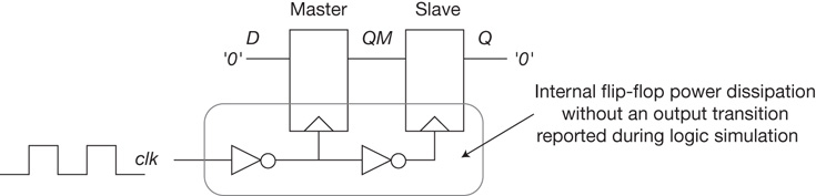
Figure 4.24 Internal cell power dissipation without a change in output value and, thus, no contribution to the signal-switching activity calculation.
The characterization of sequential cells and the power calculation flow require additional features to include the contribution from events that are not directly associated with functional validation testcase signal activity.
Noise characterization requires awareness of clock transitions. For combinational logic cells, noise characterization on input pins assumes static values on other inputs. The noise sensitivity of the data input pin of a sequential cell is maximized when the clock input pin is transitioning. The noise characterization for the data input should be thus simulated while the clock is in transition, using internal node measures for flop stability similar to those used for setup/hold simulations.
A special set of sequential cells is added to the circuit library for asynchronous interfaces. The characterization of these cells includes additional internal node measures during the data versus clock sweep circuit simulations. The calculation of metastability for these cells requires time constant measures for internal circuit nodes.[5,6]
Latches are not commonly present in an IP cell library. A design using alternating clock phase-based logic with latches (with potential path slack time borrowing in successive phases) requires special static timing analysis algorithms. If latches are present, cell characterization requires additional features—not only for setup/hold tests at path endpoints but also for the data-to-output timing arc for “clock transparent” mode value propagation.
4.4 Design for End-of-Life (EOL) Circuit Parameter Drift
The discussion on cell IP characterization in the previous section focuses on the circuit simulation testcases and measures used to provide models for electrical analysis flows. These circuit simulations utilize device and interconnect parameters from the foundry, based on process qualification wafer measurement data (with statistical distributions). Some device mechanisms during SoC operation, such as the following, lead to parameter drift:
Device Vt shifts due to “negative” bias temperature instability (NBTI for pFETs) and “positive” bias temperature instability (PBTI for nFETs)—During device operation where a high electric field is present between gate and conducting channel, a small population of free carriers enters the gate dielectric, filling available trap states, which results in an effective change in the device threshold voltage. For pFET devices, the direction of the electric field is from channel to gate, with free holes injected into the gate oxide; this is denoted as negative bias temperature instability (NBTI). For nFET devices, the direction of the electric field is from gate to channel, with free electrons injected into the oxide. As a result, for both pFET and nFET devices, the |Vt| increases over the operating lifetime. This mechanism is partially reversible during device operation, with the opposite gate-to-channel electric field direction. Also, the |Vt| parameter shift ultimately saturates.
Hot carrier effect—During device operation in saturated mode, where a high lateral electric field is present between the drain and the conducting channel, a flux of energetic carriers is also injected (locally) into the gate oxide near the drain node. The principal device model parameter impact is a reduction in the effective channel carrier mobility.
The magnitude of these parameter changes is provided by the foundry reliability engineering team. These effects are very much dependent upon local device temperature. Note that these mechanisms are especially prevalent in circuits with static DC bias currents, such as those used in mixed-signal IP.
The model characterization flows do not reflect these parameter drift mechanisms. Instead, special circuit simulations are separately pursued, typically using (high-sigma-sensitive) SRAM arrays and mixed-signal IP. The circuit sensitivities to these parameter drift changes are analyzed to assess the performance impacts over the SoC lifetime. To help with this assessment, SoC methodology flows provide additional data:
Switching activity data from functional validation tests and signal slews from static timing analysis—The duration and frequency of device operation in the high electric field modes is used to estimate the rates at which parameter drift and recovery occur.
Thermal map generated to estimate the local device junction temperature—The BTI and hot carrier effect parameter drift activation rates are highly dependent on the device temperature. The WC/BC cell characterization simulations use a junction temperature extreme. Product lifetime calculations commonly adopt an approach in which (spatial and temporal) temperature estimates are used, rather than an operating temperature extreme for the full lifetime. A temperature map of the SoC integrates the power dissipation flow calculations with the thermal resistance model of the die and package environment. The evolution of FinFET and silicon-on-insulator processes has introduced more complex local self-heating thermal resistance paths.
4.5 Summary
This chapter provides a brief introduction to cell and IP functional modeling, as well as the circuit characterization methods used to generate the model data required for SoC analysis flows. The EDA industry has established a detailed (and evolving) library cell modeling format that encompasses all this information.[7] This standard has enabled EDA vendors to release library characterization products to IP developers, whose output models can then be accepted by tools from any EDA vendor.
References
[1] Greene, B., “Catching X-Propagation Related Issues at RTL,– Tech Design Forum, February 26, 2014, http://www.techdesignforums.com/practice/technique/catch-x-propagation-issues-rtl/.
[2] Baddam, K., and Sukhija, P., “Challenges of VHDL X-Propagation Simulations,– Design and Verification Conference (DVCON) Europe, 2015. (Presentation slides available at https://dvcon-europe.org/sites/dvcon-europe.org/files/archive/2015/proceedings/DVCon_Europe_2015_TA5_2_Presentation.pdf; full paper available at https://dvcon-europe.org/sites/dvcon-europe.org/files/archive/2015/proceedings/DVCon_Europe_2015_TA5_2_Paper.pdf.)
[3] Lutkemeyer, C., “A Practical Model to Reduce Margin Pessimism for Multi-Input Switching in Static Timing Analysis of Digital CMOS Circuits,– TAU Workshop, 2015. (Presentation slides available at http://www.tauworkshop.com/2015/slides/Lutkemeyer_TAU15_PPT.pdf.)
[4] Kahng, A., “New Game, New Goal Posts: A Recent History of Timing Closure,– 52nd Design Automation Conference, 2015, http://ieeexplore.ieee.org/document/7167187/.
[5] Veendrick, H.J.M., “The Behavior of Flip-Flops Used as Synchronizers and Prediction of Their Failure Rate,– IEEE Journal of Solid-State Circuits, Volume 15, Issue 4, April 1980, pp. 169–176.
[6] Horstmann, J.U., et al., “Metastability Behavior of CMOS ASIC Flip-Flops in Theory and Test,– IEEE Journal of Solid-State Circuits, Volume 24, Issue 2, February 1989, pp. 146–157.
[7] Liberty modeling format; open source licensing is available from Synopsys: https://www.synopsys.com/community/interoperability-programs/tap-in.html
[8] Sun, S., et al., “Fast Statistical Analysis of Rare Circuit Failure Events via Scaled-Sigma Sampling for High-Dimensional Variation Space,– IEEE Transactions on Computer-Aided Design of Integrated Circuits and Systems, Volume 34, Issue 7, July 2015, pp. 1096–1109.
[9] McConaghy, T., et al., Variation-Aware Design of Custom Integrated Circuits: A Hands-on Field Guide, Springer-Verlag, 2013.
Further Research
Behavioral Modeling
An emerging behavioral modeling language for hardware simulation is SystemC. Describe how SystemC differs from both C-language and HDL semantics.
Describe the unique features required for synthesis of a SystemC model with a logic IP cell library.
Parameter Sampling for n-Sigma Characterization
The statistical distribution of a (dependent) circuit measurement due to fabrication process variations is required for characterization. The traditional method is to pursue random sampling (also known as Monte Carlo sampling) from the independent input parameter distributions and re-simulate a sufficient number of the same testcase stimuli with these different sample sets to plot a distribution of the circuit measurement. Of greatest interest are the n-sigma extremes of the measured value. More efficient methods are being pursued to reduce the number of simulations to estimate the high-sigma “tails” of the measured distribution (with high confidence).
Describe how importance sampling is applied to circuit simulations from independent parameter distributions.
Other sampling methods have also been proposed, including “scaled-sigma” sampling[8], worst-case distance, and high-sigma Monte Carlo[9]. Describe how these methods differ from importance sampling.