3
Circuits
In the design of a synchronizer the values of Tw and τ depend on the circuit configuration. Both affect the resolution time, but τ is more important for synchronization because the synchronization time needed is proportional to the resolution time constant τ. The effect of increasing Tw by a factor A is simply to add to the synchronization time an amount equal to τ ln(A).
Tw is mainly determined by the input characteristics of a latch circuit and τ is the time constant of the feedback loop. To some degree these two can be traded, a low-power input drive can reduce the loading on the feedback inverters thus reducing τ, but usually at the expense of Tw. Increasing power can often reduce both Tw and τ because the parasitic capacitances become a lower proportion of all capacitance, but only up to a point where parasitic capacitances become negligible and the value of C/G reaches a minimum.
3.1 LATCHES AND METASTABILITY FILTERS
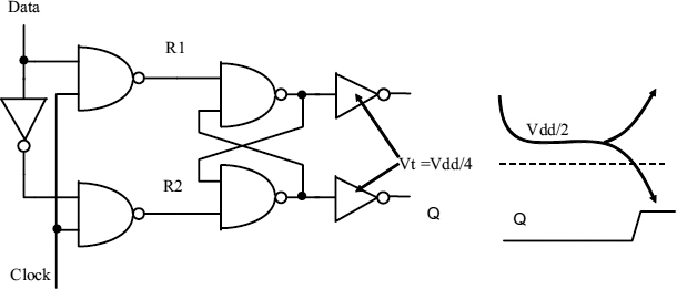
Figure 3.1 shows a simple latch made up of four NAND gates and an inverter. When the clock goes low, both R1 and R2 go high and the latch becomes opaque. Without the two inverters on the outputs a metastable level of Vdd/2 could cause any following digital circuits to malfunction when the circuit becomes metastable. The inverters on the outputs of Figure 3.1 prevent the half-level appearing at the output because they have a lower than normal threshold level. If the latch is in a metastable state, both inverter outputs are low because the output level when the circuit is metastable is higher than the output inverter threshold. Only when one latch output moves lower than the inverter threshold can the corresponding inverter output go high. The W/L ratio of the transistors in the inverters is crucial here to make low-threshold inverters. Wider n-type transistors and narrow p-type will give a lower than normal threshold, and wider p-types than n-types give a higher threshold.
Figure 3.1 Latch with low-threshold inverters.
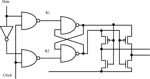
An alternative metastability filter arrangement [9] is shown in Figure 3.2, where a high output only appears when there is sufficient difference between the two latch outputs. The advantage of this is that it will filter out metastable outputs where both output voltages have the same value irrespective of whether the output voltage is, high, low, or half-level. Thus it can also be used to remove the effects of metastability in circuits like Figure 2.13 where both outputs go up and down in phase. Only when they diverge can an output appear from the filter.
Figure 3.2 Latch with metastability filter.
In Figure 3.2, when the clock goes low, one of R1 and R2 may go high just before the other, causing the latch to start to change state, but if the overlap is short the latch may be left in metastability. The NAND gate outputs both start high, but the filter outputs are low because the two p-type transistors are nonconducting
When both gate outputs go to the same metastable level, the filter outputs remain low, and as the metastability resolves, the latch outputs diverge. Only when there is a difference of at least Vt between the gate outputs can the filter output start to rise, so that one output rises when the high output gate is at about: (Vdd + Vt)/2, and the low output gate is at about (Vdd − Vt)/2.
3.2 EFFECTS OF FILTERING
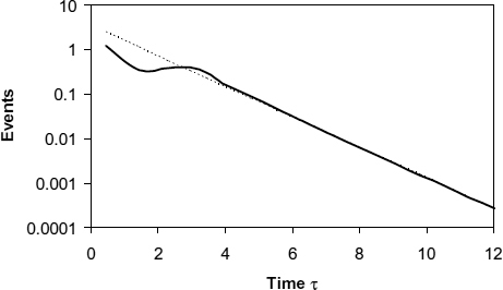
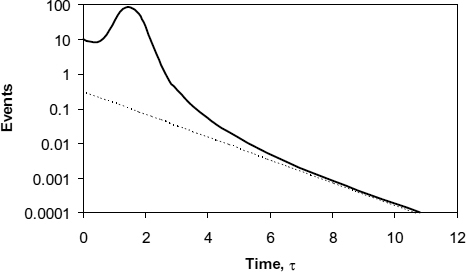
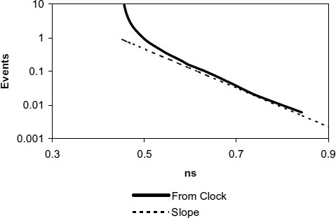
The event histograms of latches with metastability filters can be affected by the nature of the filter. When the clock in Figure 3.2 is high either R1 or R2 will be low. When the clock goes low both R1 and R2 go high. By SPICE simulations and measurements on sample circuits it is possible to find the output times for a range of input time differences between R1, and R2. Typical results are shown in the event histograms of Figure 3.3 and Figure 3.4.
Figure 3.3 Histogram for metastability filter. Reproduced from Figure 6, “Synchronization Circuit Performance” by D.J. Kinniment, A Bystrov, A.V. Yakovlev, published in IEEE Journal of Solid-State Circuits, 37(2), pp. 202–209 © 2002 IEEE.
Figure 3.4 Latch with low-threshold output inverters. Reproduced from Figure 7, “Synchronization Circuit Performance” by D.J. Kinniment, A Bystrov, A.V. Yakovlev, published in IEEE Journal of Solid-State Circuits, 37(2), pp. 202–209 © 2002 IEEE.
Figure 3.3 shows the effect of the circuit with a filter of the type shown in Figure 3.2, where the gate outputs both start high, and one of them must go more than Vt/2 below metastability to give an output. Output times in this figure are measured as the elapsed time in multiples of τ after the last input goes high. In Figure 3.3 the initial slope is only slightly faster than the final slope, but the effect is more pronounced in Figure 3.4 where the outputs are taken from low-threshold inverters with transistors sized the same as those in the filter. The threshold in the low-threshold inverters is about Vdd/30 below the metastable level.
The effect of the low-threshold inverter on the early part of the slope of Figure 3.4 can be compared with that of Figure 2.17 (low start) where the early events have been delayed because outputs both started high, and one has to fall to the threshold level before the inverter output goes high. In the long term this effect is negligible, so the histogram approaches the dotted trend line. In Figure 3.3 the slope of the trend line is slower because the loading on the latch output is greater, but the increase in delay applies equally to early and late events, so the difference between initial and final slope is not so pronounced. Though the circuit is slower, it is much less susceptible to noise, since the threshold detecting the resolution of metastability is much further away.
3.3 THE JAMB LATCH
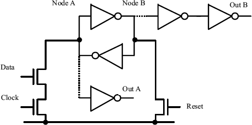
In most applications it is important to reduce the failure rate to a very low value, and therefore the value of τ should be as low as possible. Circuits called Jamb latches, based on cross-coupled inverters rather than gates are used [10,11] because inverters have a higher gain, and less capacitance, than gates. A schematic of a Jamb latch with the output taken from two places is shown in Figure 3.5.
Figure 3.5 Jamb latch.
In the Jamb latch, the cross-coupled inverters are reset by pulling node B to ground, and then set if the data and clock are both high, by pulling node A to ground. The output inverter on node A has a low threshold, and buffers the node from the effects of the output, and protects the rest of the system from the effects of metastability since its output cannot go high until node A goes fully low. It is also possible to take an output from node B, but here there must be two inverters so that the output is the same phase as the input, and two similar latches can be used in a synchronizer. The first inverter has to have a high threshold to buffer the output from metastability.
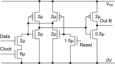
In a normal CMOS inverter, the p-type devices have a width twice the n-type. This is because it is important to make the timing of the low to high transition on the output the same as the high to low transition. To make the pull-up current from a p-type CMOS transistor the same as the pull-down current from an n-type transistor, the width of the p-type has to be twice the n-type. The situation in metastability is different. Here the transconductance of the inverter is the sum of the transconductance G, of both p-type and n-types, and the capacitance C is also the sum of both devices. Thus the optimum value of τ = C/G is found when the p-type is much smaller than the n-type, ideally zero. In practice the variation in τ with p-type width is not large, and it is necessary to have a p-type pull-up transistor to hold the latch state so a 1:1 ratio between p and n widths is usually used. For correct operation, reset, data and clock transistors must all be made wide enough, when compared to the inverter devices, to ensure that the nodes are properly pulled down during set and reset. Typically, this means that the reset transistor has a similar width to the p-type transistors in the flip-flop, and the data transistor is wider because it is in series with the clock. Typical transistor widths are shown in Figure 3.6.
Figure 3.6 Jamb latch B transistor widths.
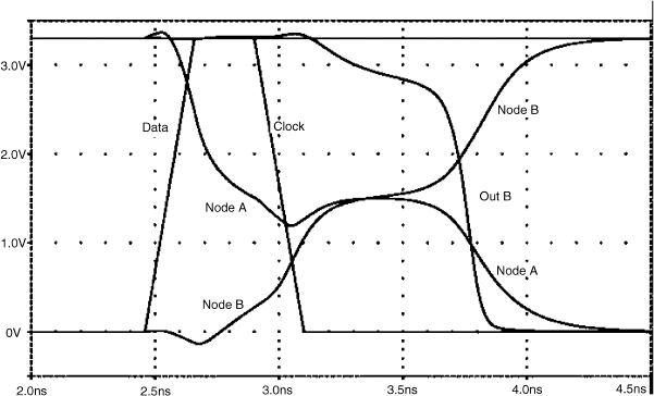
Metastability occurs if the overlap of data and clock is at a critical value which causes node A to be pulled down below the metastability level, but node B has not yet risen to that level. This can be seen in Figure 3.7, which was produced by simulation, where the data goes high at about 2.55 ns while the clock is high, then node A falls to about 1.1 V, while node B rises to about 0.8 V. When the clock input goes low at 3 ns both node A and node B become metastable at about 1.5 V, and the output can be taken from node B with an inverter whose threshold is 0.1V higher than the metastable level.
Figure 3.7 Jamb latch waveforms. Reproduced from Figure 9, “Synchronization Circuit Performance” by D.J. Kinniment, A Bystrov, A.V. Yakovlev, published in IEEE Journal of Solid-State Circuits, 37(2), pp. 202–209 © 2002 IEEE.
If the latch state is to be observed at node A, we must use a low-threshold inverter between node A and the output because that node is going low. Only one output inverter is actually connected to either node A or node B to avoid loading the latch too much, and in that inverter the transistor widths are minimized. When the node B output is used the inverter threshold and node B start voltage are on different sides of the metastable level so the events histogram should correspond to the high-start, low-threshold curve of Figure 2.17, and in the second (node A output), they are on the same side so this corresponds to the high-start, high-threshold curve. When the clock and data overlap, both nodes always start from below the metastable level. To record an output from the node A Jamb latch a low-threshold inverter is used, so that when node goes fully low, there is a high output. This node is quite sensitive to small changes in the clock data overlap, because it is already below the metastable level and does not have far to move. This means you get a bigger than expected change in output time for a given overlap change, and therefore there are fewer events that can give an output within a fixed output time slot.
The inverter on node B needs to have a high threshold to record an out-put change, and it is less sensitive to a given change in clock data overlap than would be expected, because the node is low already, and needs to go high to give the low going final output. Turning that into the number of events that fit into an output time slot, there are more than normal because a bigger change in clock data overlap is needed to span the time slot.
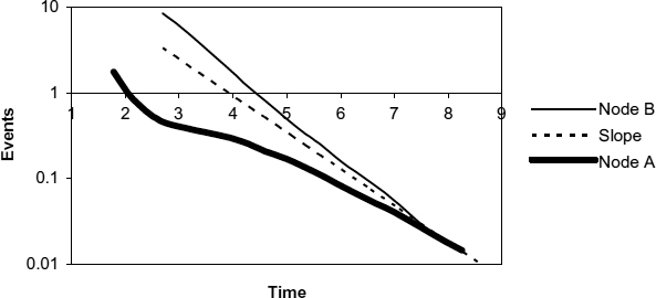
Histograms produced from simulations of both node A and node B circuits are shown in Figure 3.8. The node A circuit has both start and threshold on the same side of the metastable level, and is therefore equivalent to the high-start high-threshold case of Figure 2.17, whereas for Node B the start and threshold are on opposite sides, and so are equivalent to the low-start case.
3.3.1 Jamb Latch Flip-flop
A master–slave flip-flop built from two Jamb latches may have the latch output taken either from node A or node B. If node A is used, a single inverter with a low threshold provides a high output when the data is high and the latch is clocked.
Figure 3.8 Jamb latch histograms. Reproduced from Figure 10, “Synchronization Circuit Performance” by D.J. Kinniment, A Bystrov, A.V. Yakovlev, published in IEEE Journal of Solid-State Circuits, 37(2), pp. 202–209 © 2002 IEEE.
For large input times the two latch outputs in Figure 3.8 have a shorter delay for node A than for node B, for example in a simulation of a typical 0.18 μ process when the input is 113 ps before the clock, the output after one inverter is 97 ps after the clock for Out A, a total delay of Td = 210 ps and 147 ps after for node B so Td = 260 ps. However when the input is less than 10 ps, the delays are very similar. Intuitively, it is obvious that the large signal delay from the input through to the first Out B inverter path has one more inverters than the Out A path, and will be approximately one inverter delay longer. The simulation shows that when the clock goes high and the latch is metastable, there is very little voltage difference between nodes A and B, so the two delays are similar when metastability is resolved.
By plotting input times against output times we can deduce the values of τ, Tw0 and Td from the simulations
For Node A τ = 40 ps, Tw0 = 20 000 ps and Td = 201 ps
For Node B τ = 40 ps, Tw0 = 20 000 ps and Td = 250 ps
Here we are using Tw0 which is the intercept on the y-axis at for output times measured from the clock. Tw is the intercept for the typical output time of around 250 ps, and in this case is
![]()
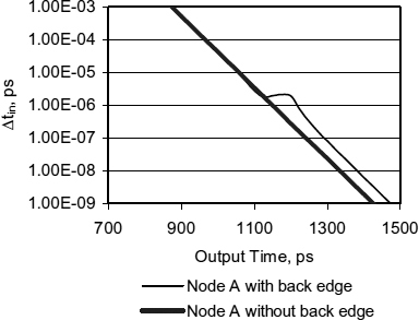
Figure 3.9 Jamb latch Out A back edge offset.
The back edge offset (Equation 2.25), for Out A is therefore, 47 ps and for Out B, −1 ps. 47 ps is similar to the delay expected in an inverter in this technology. Further simulation for a master–slave flip-flop using Node A and with a clock back edge at 1 ns gives the input output characteristic of Figure 3.9.
The difference between Td and the projection of the deep metastability slope τ, back to the point where Δ tin = τ gives an estimate of the offset.
3.4 LOW COUPLING LATCH
The value of τ in these circuits is determined by the drive capability of the inverters, and the capacitive loading on the nodes. To reduce this loading, the output inverters should have small geometry, but the set and reset drive transistors in the Jamb latch cannot be reduced below a certain size, or the circuit will not function correctly. It is possible to overcome this problem by switching the latch between an inactive (no-gain) and an active (high-gain) state. As the device moves between the two states, only a small drive is necessary to cause the output to switch one way or the other, and if this drive is small, it can be maintained in the fully active state without switching the output further.
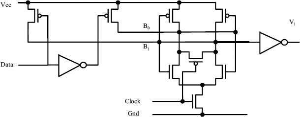
Figure 3.10 shows a circuit based on this principle, in which the latch is activated by the low to high transition of the clock, and one of the B1 and B0 nodes goes low, giving a high output on V1 if data is high before the clock. Because they don't need to overcome a fully conducting n-type transistor, the p-type data drive transistors need to be less than one-quarter the size of those in the Jamb latch, and so load the latch is much less.
Figure 3.10 Low-input coupling latch. Reproduced from Figure 12, “Synchronization Circuit Performance” by D.J. Kinniment, A Bystrov, A.V. Yakovlev, published in IEEE Journal of Solid-State Circuits, 37(2), pp. 202–209 © 2002 IEEE.
The simulated performance of the circuit is shown in Figure 3.11. The output takes at least 5τ from the clock, where the Jamb latch takes only 2τ. This is because the internal bistable starts from near the metastable point when the clock goes high, and only has a very low drive to bias it in one direction or the other, where the Jamb latch is driven very hard by any clock data overlap. The trade off is that τ is only 80% of the equivalent Jamb latch. Because τ is lower, after a resolution time of 20τ it has caught up with the Jamb latch, and the number of events at 30τ is significantly less. The trade-off is that τ has been made a little smaller, at the expense of Tw, which is significantly bigger, and hence the delays are longer at first. The value of τ in this circuit is lower because loading effects from the set and reset mechanism are lower.
Figure 3.11 Low-coupling latch characteristics.
3.5 THE Q-FLOP
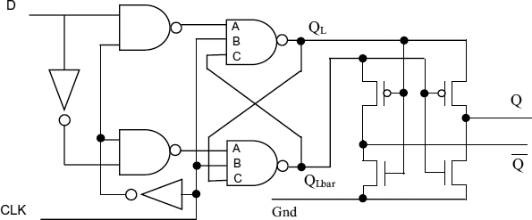
In some systems it is useful to know when metastability has resolved. In order to achieve this we can use a metastability filter in a circuit whose outputs are the same in metastability, and also when the clock is low. A circuit that has these properties is shown in Figure 3.12 This circuit, sometimes known as a Q-flop [12], ensures that half-levels will not appear at the output, and any uncertainty due to metastability appears as a variable delay time from the clock to the output rather than a half-level. When the clock is low, both outputs are low because both QL and QLbar are high. When the clock goes high the Q-flop can take up the state of the D input at that time, and then becomes opaque to D changes, but it may become metastable if the D input changes near to the clock edge time.
In Figure 3.12 only clean output level transitions occur, because the output is low during metastability, and only goes high when there is a significant voltage difference between QL and QLbar. Equation (2.5) shows that the transition between a voltage difference of V1 and V2 takes a relatively short time, τ ln (V2/V1), so when the voltage between QL and QLbar is sufficient to produce an output (more than the p-type threshold Vt) the transition to a full output of Vdd will take less than 2τ. This voltage difference is also much greater than any latch internal noise voltage, so when the QL signal leaves the metastable region to make a high transition, it happens in a bounded time and cannot return low. On the other hand, the time at which this transition takes place cannot be determined, and may be unbounded.
Figure 3.12 Q-flop.
3.6 THE MUTEX
An important component of asynchronous systems is the mutual exclusion element. Its function is to control access to a single resource from two or more independent requests. If access to one request is granted, the others must be excluded until the action required is completed. A simple application is the control of access to a single memory from two processors. Requests from each processor to read from, or write to a particular memory location must not be interrupted by the other, and if the requests are entirely independent, they may occur nearly simultaneously. The design of arbiters, which decide which request to grant are discussed more fully in Part C, but almost all are based on the use of a MUTEX circuit which must distinguish between two closely spaced requests, and metastability is inevitable when the time between requests is very close.
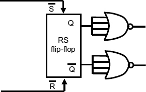
Most MUTEX circuits are based on a set reset latch model in which the latch is made from cross-coupled gates, and is followed by a filter circuit, which prevents metastable levels reaching the following circuits, and also has the function of signalling when the decision is complete. Figure 3.13 shows how this can be done with arrangement similar to Figure 3.1 in which the outputs of the RS latch are fed into two low-threshold inverters.
Figure 3.13 MUTEX.
Figure 3.14 FPGA MUTEX with low-threshold inverters.
When both request inputs, R1 and R2, of the MUTEX are low, both of the latch outputs are high. In this case both inverter outputs, G1 and G2, act as the grant outputs and are low; this signals that no request has been granted. If only one request goes high, the corresponding grant will go high, and any subsequent request on the other input will be locked out. If both requests are made within a short time of each other, the first request will normally be granted, but if both grants go high at almost the same time the latch may be left in a metastable state. In metastability both grant outputs are low because the latch metastable level is higher than the output inverter thresholds, shown here as a dotted line. Only when one latch output goes fully low can the corresponding grant go high. It is important to note that a high grant output then indicates the end of metastability in the latch and the completion of the MUTEX decision.
It is more difficult to design a MUTEX in a standard cell or FPGA environment because the transistor geometries cannot be altered to produce a shifted threshold, but a similar effect can be obtained by paralleling the inputs on a multi-input NOR gate to lower the threshold as in Figure 3.14, or using a multi-input NAND gate to raise the threshold. An FPGA MUTEX should also have the flip-flop implemented as a single RS device to avoid the possibility of the oscillation problem described earlier.
Once the latch output voltage has fallen far enough below Vdd/2 to cause one of the grant outputs to start to go high it does not take long for it to fall all the way to a defined low level. Since the output voltage trajectory of a metastable latch is given by Equation (2.5), then the time taken for the trajectory to go from a threshold level, Vth below metastability, to a low logic level Vlow, is
This time is a constant, depending only on circuit characteristics, so the timing of the end of metastability after the output gate threshold is exceeded is fixed, and the grant cannot return to a low level.
Typically MUTEX circuits are used in situations where the time between the requests R1 and R2 can have any value, and the probability of all separation times is the same. We can assume therefore that the probability of all the values of Kb between 0 and Vdd is also the same. Now the average extra time required for resolution of metastability can be found by using Equation (2.5), where
![]()
and averaging t over all values of Kb
From this it is possible to see that on, average the time penalty imposed by a MUTEX is quite short, at the normal propagation delay plus τ. While there is a finite probability of long resolution times, the probability of times significantly longer than τ decreases exponentially with time, and the probability of an infinite decision time is zero.
3.7 ROBUST SYNCHRONIZER
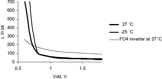
One of the problems of synchronizers in submicron technology is that latches using cross-coupled inverters do not perform well at low voltages and low temperatures. Since the value of τ depends on the small signal parameters of the inverters in the latch it is more sensitive to power supply variations than the large signal propagation delay expected when an inverter is used normally. This is because the conductance of both the p- and n-type devices can become very low when the gate voltage approaches the transistor threshold voltage VT, and consequently C/G can become very high. As Vdd reduces in submicron processes, and VT increases, the problem of increased τ and therefore greatly increased synchronization time gets worse. Typical plots of τ against Vdd for a 0.18 μ process are shown in Figure 3.15. It can be observed from this figure that τ increases with Vdd decreasing and the reduction in speed becomes quite rapid where Vdd approaches the sum of thresholds of p- and n-type transistors so that the value of τ is more than doubled at a Vdd of 0.9 V, and more than an order of magnitude higher at 0.7 V, −25°C. For comparison the typical large signal inverter delay with a fan out of four (FO4) in this technology is shown. This demonstrates τ is likely to track the processor logic delay rather poorly, making design difficult.
Figure 3.15 Jamb latch τ vs Vdd.
The increase in τ can have a very important effect on reliability. For example, a synchronizer in a system where a time equivalent to 30τ has been allowed might give a synchronizer MTBF of 10 000 years. A 33% increase for τ, in this synchronizer will cause the time tp fall to an equivalent of only 20τ. As a result the MTBF drops by a factor of e−10 from 10 000 years, to less than 6 months. It is very important, that worst-case variations of all parameters, such as process fluctuations, temperature, and power supply are taken into account in any estimate of τ to ensure that the reliability of the system under all operating conditions is as expected, and circuits are needed that are robust to variations of process, voltage and temperature.
One way of improving the value of τ is to increase the current in the transistors by increasing all transistor widths, but this will also increases power dissipation. In order to estimate the average energy used during metastability, we will assume that the average metastability time is τ. As the transistor width increases, the total switching energy increases in proportion but τ only decreases slowly as transistor sizes increase, and reaches a limit at around 30 ps in a 0.18μ process. While τ can be optimized for conventional circuits, sensitivity to PVT variation remains a problem.
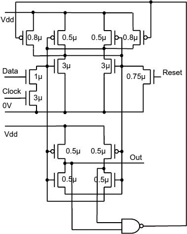
An improved synchronizer circuit [23] that is much less sensitive to power supply variations is shown in Figure 3.16.
Figure 3.16 Robust synchronizer. Reproduced from Figure 2, “A Robust Synchronizer Circuit”, by J Zhou, D.J. Kinniment, G Russell, and A Yakovlev which appeared in Proc. ISVLSI'06, March 2006, pp. 442–443 © 2006 IEEE.
This circuit is essentially a modified Jamb latch where two 0.8 μ p-type load transistors are switched on when the latch is metastable so as to maintain sufficient current to keep the total transconductance high even at supply voltages less than the sum of thresholds of the p- and n-type transistors. Two 0.5 μ feedback p-types are added in order to maintain the state of the latch when the main 0.8 μ p-type loads are turned off. Because of these additional feedback p-types, the main p-types need only to be switched on during metastability, and the total power consumption is not excessive. In the implementation of Figure 3.16 a metastability filter is used to produce the synchronizer output signals, which can only go low if the two nodes have a significantly different voltage. The outputs from the metastability filter are both high immediately after switching, and are then fed into a NAND gate to produce the control signal for the gates of two main p-types. In this circuit, the main p-types are off when the circuit is not switching, operating like a conventional Jamb latch, but at lower power, then when the circuit enters metastability the p-types are switched on to allow fast switching. The main output is taken from the metastability filter, again to avoid any metastable levels being presented to following circuits. Now there is no need for the feedback p-types to be large, so set and reset can also be small. The optimum transistor sizes for the improved synchronizer are shown in Figure 3.16, and the resultant τ at Vdd of 1.8 V is as low as 27.1 ps because the main transconductance is provided by large n-type devices and because there are two additional p-types contributing to the gain. It also operates well at 0.6 V Vdd and −25°C, because it does not rely on any series p- and n-type transistors being both switched on by the same gate voltage.
Figure 3.17 Robust synchronizer τ vs Vdd.
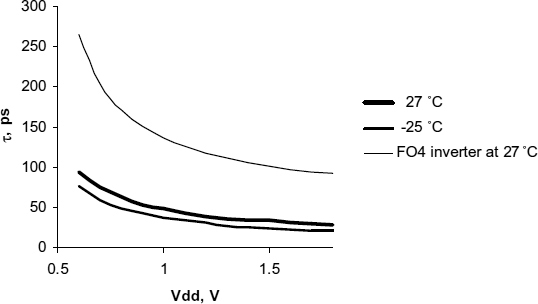
The relationship between τ and Vdd for the improved synchronizer is shown in Figure 3.17.
The switching energy for this circuit is 20% higher than a conventional Jamb latch. At the same time as maintaining a low value of τ, the ratio between τ and FO4 is much more constant at around 1:3 over a wide range of Vdd and temperature.
3.8 THE TRI-FLOP
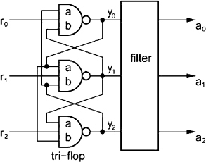
Multistable (as opposed to two state) flip-flops have also been proposed for synchronization and arbitration, and may have an advantage in some situations, however implementations can be unreliable. Figure 3.18 shows a tristable circuit, in which only one of the y outputs can be low when all the r inputs are high. Multi input MUTEX circuits can be made from trees of two or three input circuits an in certain circumstances a tree based on three input MUTEXes may be lower power and higher performance than those based on two input MUTEXes. Unfortunately without careful design they can oscillate when two, or all three request signals r0, r1, and r2 arrive simultaneously.
Figure 3.18 Tristable flip-flop. Reproduced from Figure 1, “Analysis of the oscillation problem in tri-flops”, by O. Maevsky, D.J. Kinniment, A. Yakovlev, A. Bystrov which appeared in Proc. ISCAS'02, Scottsdale, Arizona, May 2002, IEEE, volume I, pp. 381–384 © 2002 IEEE.
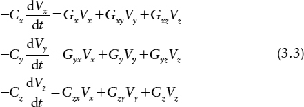
The small signal model for a tristable can be described by three first-order differential equations
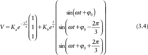
where Cx, Cy, Cz represent the output capacitances of gates x, y, and z, and Gx, Gy, Gz their output conductances. Similarly, Gxy, Gxz, etc. represent the input transconductances of gate x, etc. from the inputs connected to gates y and z. If Cx,=Cy=Cz=C, Gx=Gy=Gz=G and Gxy=Gyz=Gzx=Ga Gxz=Gzy=Gyx=Gb, a solution can be found where:
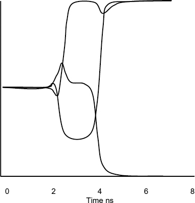
Figure 3.19 Oscillation in a tri-flop. Reproduced from Figure 2, “Analysis of the oscillation problem in tri-flops”, by O. Maevsky, D.J. Kinniment, A. Yakovlev, A. Bystrov which appeared in Proc. ISCAS'02, Scottsdale, Arizona, May 2002, IEEE, volume I, pp. 381–384 © 2002 IEEE.
Here

If the two input transconductances, Ga, Gb are consistently different, metastability may result in oscillations on the outputs, which cannot be filtered out [13]. Taking this to the extreme where Gb = 0, but Ga is not, the ‘b’ inputs to the gates would be open circuit, and we would have a ring of three oscillator. This oscillatory metastability is clearly shown in Figure 3.19 where the tri-flop was implemented using 0.6 μ CMOS ‘symmetrical’ NAND gates in which the width of the input transistors was twice that of the ‘b’ input. Realistic worst-case tolerances of technological parameters also give a similar, though less vivid effects.
If the input transistor geometries are made identical, ω becomes zero, and there is no oscillation, but small variations in the transistor critical length dimensions could easily tip the circuit into instability, and a more robust solution can be found by examining the roots of the characteristic equation

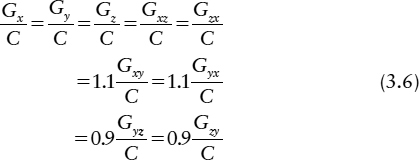
Imaginary roots will result in an oscillatory solution to the system of differential equations, but stability, with a tolerance of 10% variations in transconductance can be assured [14], by making:
The potential gain from using a tri-flop, however, is not likely to be worth the effort of ensuring the correct transconductance conditions, and networks of two-way MUTEXs will generally be more advantageous when building multiway arbiters.
Synchronization and Arbitration in Digital Systems D. Kinniment
© 2007 John Wiley & Sons, Ltd

