9
Pausible and Stoppable Clocks in GALS
Traditionally, clocks are derived from very accurate, crystal-controlled oscillators whose frequencies are fixed. Any interface between two independently clocked domains has to assume that the timing of the two clocks cannot be changed in any way, and this leads to the need for synchronizers to retime the data. In a globally asynchronous, locally synchronous (GALS) system [65,67,68], it is possible to pause, or stop the clock, rather than retime the data so that synchronization is not necessary.
There are two main methods of using the communication between processors to link the clocks. If the processor clock starts when data arrives, and activity stops as soon as the data is processed the clock is called data driven [71]. With a data-driven clock there is no choice between ongoing internal processor activity and the need to process new data, so there is no competition between them and there can be no metastable signals. A pausible clock [72,73] is normally running when the input data arrives so there is still a choice, to pause or not to pause, just before the next clock is due. Even if there is no internal processing when data arrives, requests coming from two independent sources to the same processor may have to be arbitrated. Instead of synchronizers with a fixed resolution time and a consequent probability of failure, a processor core with a pausible clock uses a MUTEX to decide if the clock should be paused in this cycle or the next. While the MUTEX is metastable, the clock is paused, the resolution time is unknown and can be unbounded, but there is no reliability problem. Pausing the clock means that the processor does nothing, but on average, the additional resolution time in the MUTEX is quite small. On average it is τ, so the loss of performance resulting from arbitration is also small.
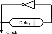
Figure 9.1 Delay-based oscillator.
9.1 GALS CLOCK GENERATORS
A simple oscillator made up from a delay and an inverter is shown in Figure 9.1, and this forms the basis of most stoppable clocks [74]. The delay itself is usually a chain of inverters and the total number of inverters in the ring is odd. This means the clock frequency is 1/2ntd where n is the number of inverters, and td is the delay per inverter.
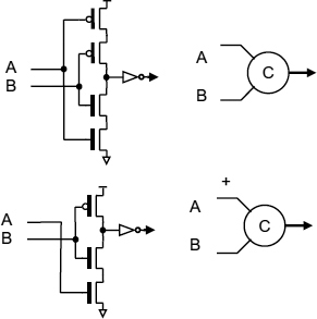
To ensure that the clock can only be stopped after a complete cycle we need a C gate [69,70] which only produces an output after all its inputs have changed. The top circuit in Figure 9.2 shows a simple design for a two-input C gate in which the output goes high after both inputs go high, and low when both inputs are low. If the inputs are different, the output will stay at its previous level. Circuits like this can also be modified so that an input is only sensitive to a positive or negative edge. In the bottom circuit the output goes high only after both the A and B inputs have gone high, but only the B input needs to go low to give a low output, so A is sensitive to the positive going edge, but not the negative edge.
Figure 9.2 C Gates.
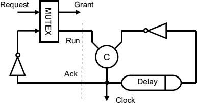
Figure 9.3 Pausible clock. Reproduced from Figure 1, “Demystifying Data-Driven and Pausible Clocking Schemes”, by R Mullins and S Moore which appeared in Proc. Thirteenth Intl. Symp. on Advanced Research in Asynchronous Circuits and Systems (ASYNC), 2007 pp. 175–185 © 2007 IEEE.
A complete pausible clock circuit is shown in Figure 9.3 [72–74]. The MUTEX outputs are both low if its inputs are both low, but if one input is high the corresponding output also goes high, leaving the other low. If both inputs go high, the MUTEX arbitrates between them. If the request was the first input to go high the grant signal goes high and run stays low, otherwise grant stays low and run goes high.
In Figure 9.3 with a low input request, the grant is always low and the run signal follows the inverse of the clock, so one input to the C gate changes when the inverse clock changes, and the other later at a time determined by the delay. As a result the clock cycles at a frequency of 1/2 Delay.
When the request signal goes high the run signal stays low if it is already low (clock is high), or goes low the next time the clock goes high. The clock cycle is completed by the other input to the C gate going low after the delay time. The clock then goes low, and a high-going edge arrives at the C gate after the delay. Because run remains low a new cycle starts. When the request goes low again, the clock is low, run goes high and a new cycle of the clock is initiated.
The clock circuit operates with a four-phase protocol:
- the request goes high, and the clock is paused;
- Ack goes low, signalling completion of the cycle;
- request is lowered, allowing the clock to continue;
- Ack goes high.
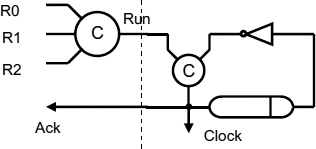
Figure 9.4 Synchronized inputs.
The alternative of a stoppable clock is shown in Figure 9.4 [71]. Here there are a number of request signals, R0, R1, and R2 indicating the arrival of a data item.
Run only goes high after all the data has arrived, and then Ack goes high. A single cycle of the clock is enforced by a four-phase protocol in which the requests are lowered, and Ack goes low after the end of the delay. A second cycle cannot start until new requests arrive and the stoppable clock is effectively synchronized to the data.
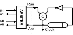
If two or more requests are competing for processor time, it is necessary to arbitrate between them. In Figure 9.5 the data-driven clock circuit is generalized to more than one input by replacing the C gate with an arbiter. Arbiters are discussed in more detail in Part III, here we assume that requests R0 and R1 arrive independently, and one is granted. The run signal then initiates a single clock cycle.
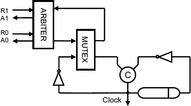
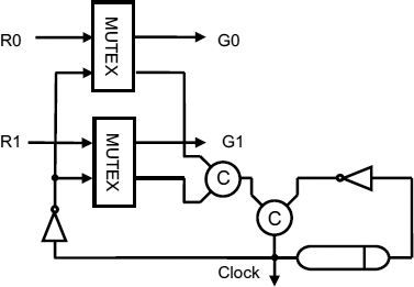
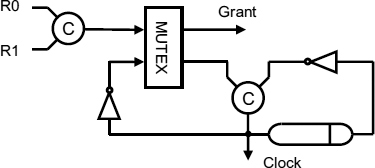
An arbiter can also be used as the input to a pausible clock as in Figure 9.6. In this circuit, as soon as the grant is made the request that succeeded is acknowledged. Pausible clocks which simply sample the request inputs every cycle, or wait for all requests to be present, are shown in Figure 9.7 and Figure 9.8.
In Figure 9.7 either R0 or R1 can pause the clock. The clock will not start again until the request is cleared, but in Figure 9.8 both R0 and R1 must be present before the clock is paused.
Figure 9.5 Arbitrated inputs. Reproduced from Figure 2, “Demystifying Data-Driven and Pausible Clocking Schemes”, by R Mullins and S Moore which appeared in Proc. Thirteenth Intl. Symp. on Advanced Research in Asynchronous Circuits and Systems (ASYNC), 2007 pp. 175–185 © 2007 IEEE.
Figure 9.6 Pausible clock with arbitrated inputs. Reproduced from Figure 4, “Demystifying Data-Driven and Pausible Clocking Schemes”, by R Mullins and S Moore which appeared in Proc. Thirteenth Intl. Symp. on Advanced Research in Asynchronous Circuits and Systems (ASYNC), 2007 pp. 175–185 © 2007 IEEE.
Figure 9.7 Pausible clock with sampled inputs. Reproduced from Figure 4, “Demystifying Data-Driven and Pausible Clocking Schemes”, by R Mullins and S Moore which appeared in Proc. Thirteenth Intl. Symp. on Advanced Research in Asynchronous Circuits and Systems (ASYNC), 2007 pp. 175–185 © 2007 IEEE.
Figure 9.8 Pausible clock with synchronized inputs. Reproduced from Figure 4, “Demystifying Data-Driven and Pausible Clocking Schemes”, by R Mullins and S Moore which appeared in Proc. Thirteenth Intl. Symp. on Advanced Research in Asynchronous Circuits and Systems (ASYNC), 2007 pp. 175–185 © 2007 IEEE.
As well as stopping or pausing the clock when an input request arrives, the clock may have to be to be stretched when output data has not been acknowledged, that is, the clock must remain low until output is complete.
9.2 CLOCK TREE DELAYS
The plausible and stoppable clock circuits described above rely on the clock tree delay being small. That means when the clock stops, the processor will stop in a relatively short time. In practice many synchronous processor designs are large and have a clock tree consisting of many stages to provide the drive necessary for a large system [75,76]. In a synchronous system the clock never stops so it does not matter that the delay through the clock tree is a large proportion of the clock cycle time provided that each edge arrives at the same time in all parts of the processor. If the clock has to be started and stopped by requests for a data transfer, all clock edges are associated with data, and it is important that the data and the clock edges that deal with that particular data item are timed to arrive at the same time.
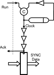
Figure 9.9 shows how the insertion of a clock tree may affect the latching of data into the processor input register. In Figure 9.9 the clock tree is shown as a chain of buffers between the oscillator and the point where the input register is clocked. The clock is started when the run signal goes high, but there is a delay between the starting of the clock and its arrival at the input register. Because of this delay, the input request cannot be acknowledged until the data is safely clocked into the input register, thus delaying the data transfer by at least the amount of the clock tree delay. In many processors this delay is more than half the clock period, and it can be as much as several clock cycles in a large processor. Because the Run request cannot be removed until the acknowledge is sent, the clock cycle will be extended to at least twice the clock tree delay rather than twice the delay line time.
Figure 9.9 Effect of a clock tree delay. Reproduced from Figure 11, “Demystifying Data-Driven and Pausible Clocking Schemes”, by R Mullins and S Moore which appeared in Proc. Thirteenth Intl. Symp. on Advanced Research in Asynchronous Circuits and Systems (ASYNC), 2007 pp. 175–185 © 2007 IEEE.
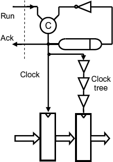
A simple solution to this problem for clock trees of less than one cycle time delay is shown in Figure 9.10 where the input data is clocked into a register by a clock unaffected by the tree delay, and then into the processor input register by a clock derived from the clock tree. The acknowledge can then be sent out much earlier, and the additional delay before the input data is usable by the processor may sometimes be used to do some pre-processing between the two registers. Effectively there are then two clock trees, the first is lightly loaded and drives the input register, and the second, loaded with the bulk of the processor clock burden, has a bigger delay of up to one clock cycle. The time between the data arriving in the first register and being clocked into the second may not be wasted, as it can be used to do some initial processing. Unfortunately this means that some redesign of the core processor may be necessary, which reduces the usefulness of a GALS system in reusing synchronous designs.
Figure 9.10 Offsetting the clock tree delay. Reproduced from Figure 11, “Demystifying Data-Driven and Pausible Clocking Schemes”, by R Mullins and S Moore which appeared in Proc. Thirteenth Intl. Symp. on Advanced Research in Asynchronous Circuits and Systems (ASYNC), 2007 pp. 175–185 © 2007 IEEE.
If the clock tree delay is more than one cycle, it is necessary to break the request acknowledge handshake to the previous processor and buffer the data by inserting a FIFO in the data path. The number of registers in the FIFO must be at least equal to the number of rising clock edges in the clock tree at any time. New data waits in the FIFO for this number of cycles before being read into the processor, and there must be a guarantee that the delay between the entry of data into the FIFO and its arrival at the head of the FIFO is short enough to allow it to be read on the correct clock cycle.
This form of FIFO based buffering allows a high data rate, but introduces latency in the communication path at least equal to the clock tree insertion delay.
9.3 A GALS WRAPPER
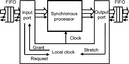
In a stoppable or pausible clock GALS environment the synchronous core processors are embedded into an asynchronous communications framework by means of a wrapper which handles the input and output ports and the starting and stopping of the local clock [77]. An overview of such a wrapper is shown in Figure 9.11. FIFOs are used to buffer both the input and the output data, but for the FIFO a two-phase handshake is shown rather than a four-phase handshake protocol, so the arrival of new data at the input port is represented by a change in level on the input request signal, and the corresponding acknowledgement is represented by a change on the input acknowledge signal. The interface to the local clock is four-phase, with the availability of new data being signaled by a high level on the Request line, and acknowledged by the Grant signal.
Figure 9.11 GALS wrapper. Reproduced from Figure 10, “Demystifying Data-Driven and Pausible Clocking Schemes”, by R Mullins and S Moore which appeared in Proc. Thirteenth Intl. Symp. on Advanced Research in Asynchronous Circuits and Systems (ASYNC), 2007 pp. 175–185 © 2007 IEEE.
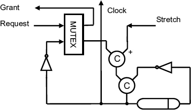
Figure 9.12 Local clock. Reproduced from Figure 10, “Demystifying Data-Driven and Pausible Clocking Schemes”, by R Mullins and S Moore which appeared in Proc. Thirteenth Intl. Symp. on Advanced Research in Asynchronous Circuits and Systems (ASYNC), 2007 pp. 175–185 © 2007 IEEE.
Figure 9.12 shows the local clock circuit where a request pauses the clock. The clock restarts when the request signal is lowered, but when the synchronous core has new data to pass to the output FIFO, it may not be accepted immediately. In that case the output request and output acknowledge signals will have different levels, one high and the other low, and the output clock cycle must be stretched until such time that data is accepted. A stretch signal is produced which is low when the output handshake is incomplete, and a C gate with one input sensitive only to positive going edges is used to stretch the clock cycle.
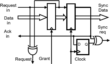
The input port of the wrapper is shown in Figure 9.13. Valid data arriving at the head of the input FIFO generates a request, the clock is paused and the data is latched into the input register. At this point the request signal to the local clock is lowered, and the clock restarts, passing synchronized data to the core processor. On the following clock an acknowledge edge is sent to the FIFO ready for the next data transfer.
Figure 9.13 Input port. Reproduced from Figure 10, “Demystifying Data-Driven and Pausible Clocking Schemes”, by R Mullins and S Moore which appeared in Proc. Thirteenth Intl. Symp. on Advanced Research in Asynchronous Circuits and Systems (ASYNC), 2007 pp. 175–185 © 2007 IEEE.
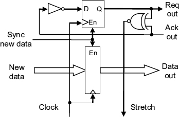
Figure 9.14 Output port. Reproduced from Figure 10, “Demystifying Data-Driven and Pausible Clocking Schemes”, by R Mullins and S Moore which appeared in Proc. Thirteenth Intl. Symp. on Advanced Research in Asynchronous Circuits and Systems (ASYNC), 2007 pp. 175–185 © 2007 IEEE.
In the output port, Figure 9.14, valid new data is clocked into a register when it is available, and the request out set to the inverse of the acknowledge out. The stretch signal then goes low until the output FIFO has latched the data forcing the clock to stretch. When the data out is acknowledged the clock resumes.
Synchronization and Arbitration in Digital Systems D. Kinniment
© 2007 John Wiley & Sons, Ltd

