7
Synchronizers in Systems
The function of a synchronizer is to re-time the data passing from one digital processor (the sender) to another (the receiver), so that it can be correctly interpreted by the receiver. This is only necessary when the sender and receiver are independently timed and even then only when their relative timing is unpredictable. For many systems on silicon it is difficult to provide a common clock at a high frequency with low skew, so independent clocks are used for each processor. Even if the clock frequency is nominally the same for both sender and receiver in some cases the requirement to re-use processors and IP blocks in new designs or different fabrication processes will often mean the actual clock frequency in any future implementation may not even be known.
7.1 LATENCY AND THROUGHPUT
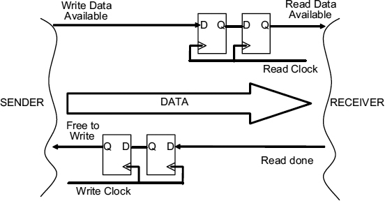
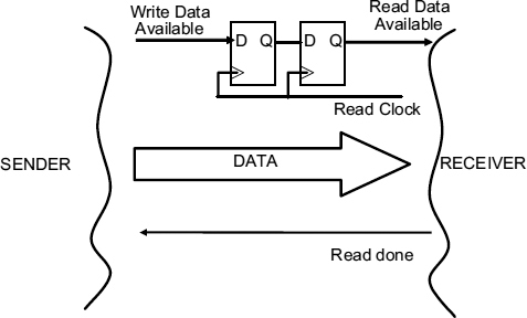
A very general synchronizing interface is shown in Figure 7.1 which allows for re-timing as the data as well as some simple flow control to ensure that the data rates on both sides of the interface are matched. Each separately timed data item is accompanied by a write data available signal from the sender which indicates that it valid data is present. Since the data available signal originates from the sender it must be synchronized to the receiver clock before it can be recognized. The receiver then transfers the data to an internal register when it is ready, and signals back to the sender that it is safe to send another data item by means of the ‘read done’ signal. Because the read done signal originates from the time frame of the receiver, it must also be synchronized to the time frame of the sender before it can be understood, and then another item can be sent.
Figure 7.1 Synchronizing interface.
In Figure 7.1 the resolution time of the synchronizer is the delay between the rising edges of the two successive clocks. Normally just one cycle time of the clock is allowed for synchronization. If both sender and receiver are synchronous there will be between 0 and 1 cycle of the read clock between the arrival of data available, and the next read clock then one cycle might be allowed for the synchronizer resolution time. If the time for a single cycle is not sufficient to give a good enough reliability it may be necessary to use two or more cycles for resolution of metastability. With a resolution time of t, a read clock frequency of fr, and a write clock frequency of fs there is a delay of between t.fr and t.fr + 1 cycles of the read clock before the data can be read as a result of synchronization. When the data is read there is a further delay of between t.fs and t.fr + 1 cycles of the write clock before the next data item can be sent. Often the two clocks have the same frequency, and the time allowed for synchronization is a single cycle. In this case there is a latency of 1–2 cycles, and a minimum turnaround time of 2–4 cycles.
The reliability of the synchronizer depends on the time allowed for metastability to settle. In terms of the metastability time constant, τ of the flip-flop, increasing the delay by a time dt increases the MTBF by a factor of edt/τ, and in order to keep system failures to less than 1 in 108 s (3 years) the total settling time may need to be over 30τ. Since τ is comparable to a gate delay, and high-performance systems may need a clock cycle of less than 10 gate delays, 30τ may be equivalent to several clock cycles. As an example if τ = 50 ps then two clock cycles at 1 GHz are required. Using n clock cycles for synchronization leads to a latency of n to n + 1 cycles, and a minimum turnaround time of 2n to 2n + 2 cycles in this simple synchronizer, so that in the worst case the transmission throughput is reduced by a factor of 2n + 2 when compared with the synchronous case.
There are two ways that a multi-cycle synchronizer can be implemented. One is to divide down the clock frequency by a factor n, and use this reduced clock frequency to drive a simple two-flip-flop synchronizer as in Figure 7.1 so that the resolution time is increased to two cycles, and the other is to pipeline the synchronizer as shown in Figure 7.2. In this scheme any remaining metastability from the first stage of the synchronizer is simply passed on to the second stage for resolution while another sample can be taken for the first stage. The advantage of the pipelined scheme is that read operations can be overlapped, but its disadvantage is that the reliability may be marginally lower as a result of the back edge effect. Because metastable conditions are passed from one stage in the pipeline to the next the MTBF after n stages of the pipeline is proportional to ent/τ, where t is the resolution time for each stage. MTBF increases exponentially with the number of stages, n, in the same way as the one stage synchronizer would with a resolution time of n.t The difference is that there is an additional edge effect when the clock goes high, and the first latch of each of the pipelined stages goes from transparent to opaque. This effect is usually small, but each extra stage introduces one more back edge delay.
Throughput can be increased by using an intermediate FIFO to separate the read and write operations, but the total time between generation of the data and its availability in the receiver cannot easily be improved. As a result, considerable latency is added to the data transmission between separately clocked zones, and this latency can be a problem, particularly in long paths where a computation cannot proceed until a requested result is received.
Figure 7.2 Two-cycle pipelined synchronizer.
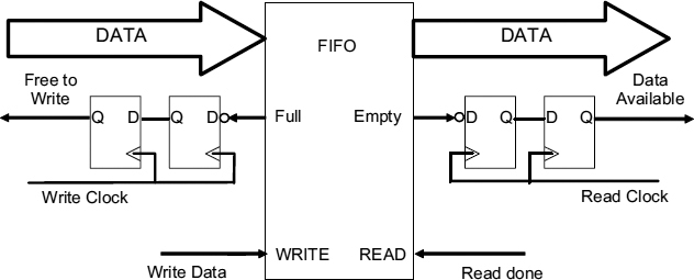
Figure 7.3 Synchronizer with FIFO.
7.2 FIFO SYNCHRONIZER
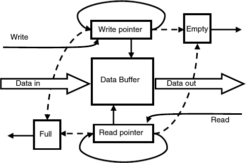
A synchronizer with a FIFO between the sender and the receiver is shown in Figure 7.3, [25–27]. The effect of the FIFO is to decouple the reading and writing processes so that writing to the FIFO can take place immediately if the FIFO has space available, and reading from the FIFO can be done as soon as the receiver is ready provided there is always some valid data in the FIFO. Because of that the throughput is no longer limited by the round-trip delay of the flow control signals, data available and read done, it can be as high as the FIFO can support. The FIFO itself is normally implemented as a circular set of registers with two address pointers, a read pointer, and a write pointer, as shown in Figure 7.4. The write pointer always points to a free location in the FIFO, and immediately after the data is written in, the pointer is advanced by one. The read pointer always points to valid data that has previously been written, and is also advanced by one immediately after the read operation. To ensure that the writer always points to a free location there must be sufficient space in the FIFO to accommodate any stored data plus the current free location and a further free location to ensure that the write pointer can be moved on without interfering with a read operation. Similarly there must be sufficient stored data to ensure that a read operation can be carried out, and the read pointer moved to new valid data. The write pointer is thus always ahead of the read pointer by at least two locations.
The flags Empty and Full are set by comparing the two pointers. Full is true if there is not sufficient space to accommodate any data items that might be written before the sender can be stopped, and Empty, which is true if there is not enough of unread items in the FIFO that might be read before the receiver can be stopped. The read pointer to write pointer distance necessary depends on the delay in stopping the receiver, and the write pointer to read pointer distance depends on the delay needed to stop the sender.
Figure 7.4 FIFO buffer.
Because the write pointer moves with the write clock and the read pointer moves with the read clock, the Full and Empty flags are not synchronized to either of the two clocks and a synchronizer must be inserted between the Full signal and the sender to ensure it is correctly interpreted. Similarly a synchronizer must be inserted between the Empty signal and the receiver. An n cycle delay in the empty signal synchronizer means that the receiver cannot be stopped for n cycles, and so there must be at least n valid data items in the FIFO. This does not affect the throughput because the delay of n cycles required to synchronize the Empty signal is overlapped with the reading of these n items. Similarly with n spaces the writes can also be overlapped with the synchronization of Full. This scheme does not improve the latency, because the time between writing an item, and reading it is at least n cycles of the read clock plus between 0 and 1 cycle for the Empty signal before further reads can be stopped. Similarly between n and n + 1 cycles of the write clock are needed to recognize that the FIFO needs another item. Forward latency (the time between data leaving the sender, and arriving at the receiver) can only be reduced by reducing the time needed to synchronize the Empty signal, and reverse latency (the time between the receiver asking for more data and the data being sent) by reducing the Full synchronization time.
7.3 AVOIDING SYNCHRONIZATION
If the clocks are all phase locked, there is no need for resynchronization of data passing between from one core processor to another, since data originating in one clock domain and passing to the next will always arrive at the same point in the receiving clock cycle. Even if the phase difference is not the same, and may not be known until the clock has run for some time, it is still predictable, and a suitable data exchange time can be found [28, 29].
A simple way to deal with a mesochronous interface, that is, one between clocks derived from a common source, is to use a FIFO [31, 32], as in Figure 7.3. If the FIFO is half full, we ensure that the sender writes one data item into the FIFO every clock period, and the receiver reads one data item every clock period. The distance between pointers cannot now move more than one from the half-full condition, and given sufficient registers in the FIFO the empty and full conditions never need to be tested. No synchronization is necessary.
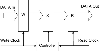
A simpler interface for mesochronous systems is shown in Figure 7.5. Here only three registers are needed even when the read and write clocks differ by an unknown (but bounded) phase difference. There is a register W for write data, an R register for read data, and an intermediate register X which must be clocked at least tset-up + tprop after the write clock, and at least thold + tprop before the read clock where tset-up, tprop, and thold are the set-up time, propagation time and hold time for the registers.
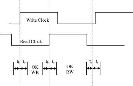
Putting ts for tset-up + tprop and th for thold + tprop Figure 7.6 shows the timing for the register X clock. There are two time intervals where the X clock can be placed. If it is put the first half-cycle of the write clock, new data is written immediately before reading (WR), if it is in the second half cycle data written in the previous cycle is read before writing new data into the X register (RW). Both of these modes allow correct transfer.
Figure 7.5 Mesochronous interface. Reproduced from Figure 2, “Efficient Self-Timed Interfaces for crossing Clock Domains”. by Chakraborty, and M. Green-street, which appeared in Proc. ASYNC2003, Vancouver, 12 – 16 May 2003, pp. 78–88., © 2003 IEEE.
Figure 7.6 Clock timing for register X.
The time interval from one rising edge of the write clock to the next is exactly one clock period, and no matter what the phase relationship between the write and read clocks, there will always be a single rising edge of the read clock within the write cycle. In order to allow a correct transfer when writing before reading there must be a time ts between the write clock rising edge and the X clock. Similarly there must be a time ts between the X clock and the next read clock rising edge. If the mode used is read before write, there must be a time th between the read clock rising edge and the X clock. Similarly there must be a time th between the X clock and the next write clock rising edge. The relative size of the two OK intervals will depend on the phase relationship between the write clock and the read clock, The time intervals OKWR and OKRW both vary according to the phase difference between read and write clocks, but the total amount of time for both OK intervals is tc − 2(th + ts) and provided that tc > 2(th + ts) at least one of them is always available.
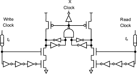
Figure 7.7 shows a circuit which can be used to control the X Clock rise time. It consists of two self resetting latches [33], one set ts after the write clock goes high, and the other set th after the read clock goes high. When both are set, the X clock goes high, thus the X clock occurs th after the read clock if the write clock is first, and ts after the write clock if the read clock is first. Neither latch can be reset until three inverter delays after the last latch was set, so the X clock lasts for three inverter delays.
Figure 7.7 X clock controller. Reproduced from Figure 4, “Efficient Self-Timed Interfaces for crossing Clock Domains”. by Chakraborty, and M. Greenstreet, which appeared in Proc. ASYNC2003, Vancouver, 12 – 16 May 2003, pp. 78–88., © 2003 IEEE.
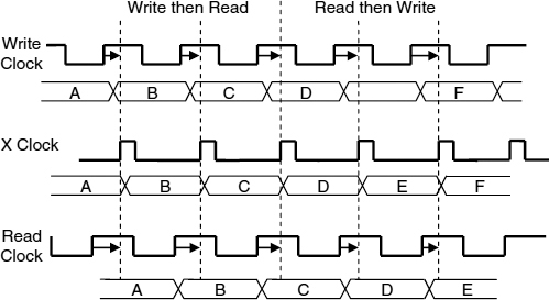
The circuit automatically adjusts to changing write–read phase, as can be seen in Figure 7.8. On the left-hand side of Figure 7.8 the write clock is ahead of the read clock, but on the right-hand side the read clock is ahead. The X clock is always generated after both read and write clocks so the circuit is not required to make a decision and consequently there can be no metastability. There is always a latency of approximately one cycle between the input data and the output data.
This scheme can also be used for multiple clock frequencies, provided they are all locked to the same root clock, which is a rational multiple of each. The data transfers can then be done by using a locally generated version of the root clock on each side of the interface.
Figure 7.8 Drifting phase. Reproduced from Figure 5, “Efficient Self-Timed Interfaces for crossing Clock Domains”. by Chakraborty, and M. Greenstreet, which appeared in Proc. ASYNC2003, Vancouver, 12 – 16 May 2003, pp. 78–88., © 2003 IEEE.
7.4 PREDICTIVE SYNCHRONIZERS
In a plesiochronous system the two clock frequencies on each side of the interface may be nominally the same, but the phase difference can drift over a period of time in an unbounded manner. If the phase difference changes by more than a cycle the simple mesochronous interfaces described above will either repeat data items or lose data items so it is necessary to use some form of flow control. In most cases the two clocks are both driven from very stable crystal oscillators and are to some extent predictable in advance. In this case synchronization can be achieved by predicting when conflicts might occur, and avoiding data transfers when the two clocks could conflict [30, 34, 35].
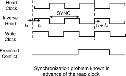
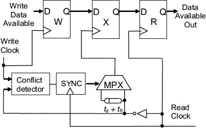
If the phase change between read and write changes very slowly, it can be detected well before any likely conflict, and this is usually the case with crystal-controlled clock generators. In Figure 7.9 the write clock edge is moving slowly later every cycle when compared with the inverse read clock, which we will use to clock an intermediate X register in Figure 7.10.
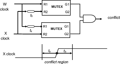
When the write clock rising edge gets to within a time ts ahead of the inverse read clock we detect a possible future conflict between the clocking of the W and X registers. The conflict signal is synchronized to the read clock, and can be used to avoid actual conflict in future by delaying the inverse read clock by ts + th. The conflict detection circuit is shown in Figure 7.11 where one MUTEX is used to detect if the write clock is more than th later than the read clock, and a second MUTEX detects if the write clock is less than ts ahead of the read clock.
Figure 7.9 Predicting conflicts.
Figure 7.10 Avoiding conflicts.
If both of these conditions are true, there will be a potential conflict. Either of the MUTEXs could produce a metastable output, so the conflict output itself must be synchronized to the read clock to ensure adequate reliability. Figure 7.10 shows how the conflict detection is integrated into a simple interface. The write data available signal is first clocked into the W flip-flop by the write clock. The conflict detector compares the W clock and X clock for potential conflicts, and the conflict signal is synchronized to the read clock. If the X clock and W data are not likely to violate the X flip-flop set-up or hold times it can be used to clock the X flip-flop. If it is likely to be within the conflict window it is delayed by at least ts + th, so that the W clock and the X clock cannot conflict. The data available signal is then clocked into the R register when the next read clock occurs. Since there is no metastability, the delay between the write data available and the read data available is between a half and one and a half cycles, even though there is a two-cycle delay between detecting a conflict and changing the X flip-flop clock timing. The correct operation of this system depends on phase changes over two clock cycles being very small, and it can be used as part of the flow control for data in a FIFO interface giving an average gain of half a cycle in latency over a single cycle synchronizer, and considerably more over a multi-cycle synchronizer.
Figure 7.11 Conflict detection.
In a predictive synchronizer of this type there is a trade-off between the sizes of the set-up and hold window, the clock cycle time, and the amount of drift, jitter and noise in the clock cycle that can be tolerated. If the clock drift, jitter and noise is large compared with the cycle time less the set-up and hold time the design of predictive synchronizers becomes more difficult.
7.5 OTHER LOW-LATENCY SYNCHRONIZERS
In practice it may be difficult to achieve accurate and reliable locking between all the clock domains because of jitter and noise in the clock generation circuit, particularly if two different frequencies must be locked together.
Other problems include cross-talk between the data and the clock tree connections introducing noise into both, and dynamic power supply variations between different parts of a clock tree and the data distribution affecting the path delay difference. Temperature changes may also alter the relative phase delay of two clock trees designed in different ways.
All of these effects cause unpredictable variation in the time of arrival of a data item relative to the receiving clock, which is particularly noticeable in high-performance systems using processor cores with large clock trees, and this is likely to increase with smaller geometries [36, 38–41]. Design of interfaces becomes more difficult as these uncertainties increase as a proportion of the receiving clock cycle and it may be simpler to assume that the two domains are independent.
7.5.1 Locally Delayed Latching (LDL)
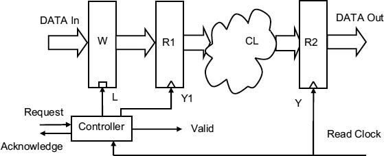
Schemes like that of Section 7.2 guarantee to deliver synchronized data to a processor core after a latency which depends on the synchronization delay. High-performance systems need at least one clock period for the synchronization time because they have fast clocks and high data rates so, this is an efficient solution, but the majority of applications have lower performance requirements. At low data rates and low clock frequencies the synchronization delay needed to maintain good reliability can be significantly less than the clock cycle time, so synchronization can be combined with some early processing in a single clock period in the first stage of the receiver pipeline. This is done by locally delayed latching [37].
An LDL circuit is shown in Figure 7.12, where the input data is first latched into a register while the controller resolves conflicts between the write request and the read clock. A MUTEX within the controller must decide whether the request occurred before the read clock rising edge, in which case the data is valid, and the next cycle of the read clock can be used for processing, or if it occurred after the read clock, in which case the data is held in the latch ready for the next clock and valid is false. Conflicts may cause this decision to take some time, and in the worst case the the request wins, but the rising edge of the signal Y1, which clocks the data held in the latch into register R1 is delayed significantly. The time available for processing this data before the next read clock rising edge is then reduced by the controller delay time plus the metastability time of the MUTEX, and any combinatorial logic delays between R1 and R2 must be complete within this reduced synchronization time.
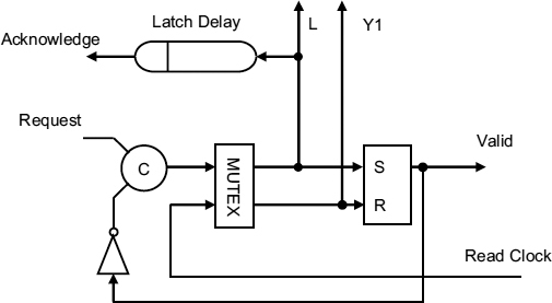
An implementation of a simple LDL input port is shown in Figure 7.13.
In this figure the MUTEX decides between a request and the clock rising edge. If the request wins, the latch is shut to hold the data, and a valid signal sent to the processor. After a delay, to ensure that the input data is captured in the latch, an acknowledgement is sent to the write processor, and the request signal is lowered. The C gate output now falls, and when the clock goes high data is clocked into R1. Valid can now be lowered and acknowledge lowered ready for the next request.
Figure 7.12 LDL circuit.
Figure 7.13 Simple input port controller.
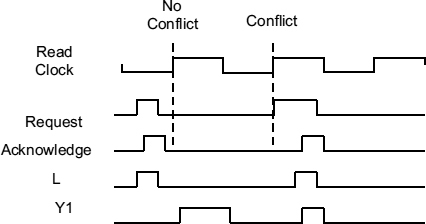
The waveforms are shown in Figure 7.14. Requests can only be accepted when the read clock is low so that they can be processed as soon as it goes high. The first clock rising edge in the figure does not conflict with a request and so can be accepted without any additional dleay. Here L rises after the request latching the data, the request is acknowledged, and L falls when valid is high and request low. When the read clock goes high the data can be clocked into the R1 register.
Figure 7.14 Controller waveforms.
The second rising edge conflicts with a request, so that the L signal is delayed by metastability, and consequently the acknowledge is also delayed. Y1 cannot be generated until valid rises after L has gone high, so the rising edge of Y1 occurs later as a result of the resolution of the conflict. This sets a limit on the time allowed for resolution, in this case a little less than half a cycle, and the remainder of the clock cycle is available for the combinational logic to carry out some processing.
The overall latency of this scheme is therefore between 0 and 1 cycle to get the input data into the latch, plus a half-cycle for synchronization. We do not count the second half-cycle because the processor is doing useful work at this time. This compares with between 0 and 1 cycle plus one cycle for a simple synchronizer, where nothing useful can be done until the data is completely synchronized. In a low-performance system where the simple synchronizer usually uses a complete cycle to clock a two-flip-flop synchronizer this can be a worthwhile saving in a system where the clock cycle time is long compared with the combinatorial logic time. Variants of the LDL controller can allow for the synchronization plus processing time of the first half-cycle to be allocated in different ways, but the failure rate depends in the end on how much time is allowed for the MUTEX to resolve conflicts. A proportion of the conflicts will always fail because of the bounded time constraint of the clock cycle, and the value of τ for a typical MUTEX is usually worse than that for a well-designed synchronizer flip-flop.
7.5.2 Speculative Synchronization
Very long metastability times occur only rarely, so by assuming that the synchronization time does not normally need to be long, and allowing for recovery from any errors if an event with a long metastability time occurs, the average latency can be considerably reduced. One possible scheme is given below.
7.5.2.1 Synchronization error detection
If the synchronization delay between the read clock and the delayed read clock is reduced the latency is improved, but the probability of failure for each data transmission will be much higher, for example for a 10τ reduction in the resolution time there would be a 22 000 times increase in failures, so a 3 year failure rate is reduced to a little more than an hour.
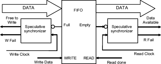
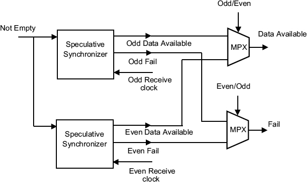
If it were possible to later detect the cases where synchronisation failed, and recover by returning to the system state before failure, the performance of the system could be improved with little penalty in reliability. Note that this does not eliminate the metastability problem, because there will still be cases where metastability lasts longer than the failure detection mechanism allows, and the system state will not be recoverable. Figure 7.15 shows how this can be done by replacing both conventional n-cycle synchronizers with speculative versions in which the data available, or free to write signals are produced early, and allowed to proceed if they subsequently prove to be correct. However, if there is any doubt about their validity at a later time, the R Fail or W Fail flag is raised so that computation can be repeated.
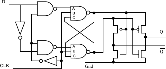
In the speculative synchronizer the first flip-flop must be tested to detect whether it has resolved in a short time or whether it will take longer than average. In order to achieve this we must use a flip-flop which always starts from a known level, and indicates when it has resolved by a monotonic transition. A latch which behaves in this way is the Q-flop described in [43], Figure 7.16, and earlier in Section 3.5. This ensures that half-levels will not appear at the output, and the uncertainty due to metastability appears (in the case of the read synchronizer) as a variable delay time from the read clock to the Q outputs.
Figure 7.15 Low-latency synchronization.
Figure 7.16 Q-flop.
In the Q-flop only clean level transitions occur, because the output is low during metastability, and only goes high when there is a significant voltage difference between Q and ![]() .
.
Once this voltage difference reaches V1, the transition between a voltage difference of V1 and V2 takes a defined time, τ ln V2/V1 so when it is sufficient to produce an output (more than the p-type threshold Vt) the transition to a full output of Vdd will take less than 2τ. On the other hand, the time from the clock at which this difference reaches V1 cannot be determined, and may be unbounded.
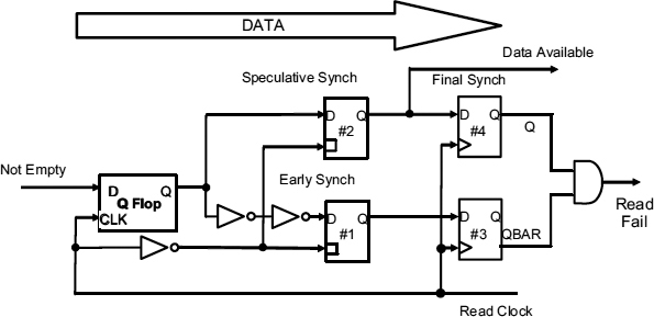
The first flip-flop in a speculative synchronizer is made up of a Q-flop latch, and two further latches, #1 and #2 as shown in Figure 7.17. The Q-flop is the master, and the two subsequent latches are slaves clocked by the inverse of the read clock. Because the output of the Q-flop is delayed by two inverters, at the time the clock goes low, latch #1 has slightly earlier version of the Q output than latch #2. Since the Q-flop always starts at a low level, the earlier version will still be low if there is any possibility of latch #2 going metastable.
Figure 7.17 Speculative synchronizer.
We will assume that when the read clock next goes high, the outputs of latches #1 and #2 are stable, an assumption that is true to a high degree of probability. At this point they are clocked into flip-flops #3 and #4 which make up the second part of the synchronizer. Because flip-flop #4 must be high if flip-flop #3 is high, there are only three digital possibilities to consider. These three combinations, together with the possibility of metastability when the next read clock occurs are shown in Table 7.1.
In Table 7.1 the first line shows the case where the synchronizer is still metastable after one clock cycle. If the read clock period is designed to give a normal synchronizer probability of being metastable, say e−30 failures per clock cycle it will be regarded as low enough to be discounted. If the early and speculative samples in flip-flop #3 and flip-flop #4 are both 0, we can infer that there was no data available signal, and the speculative output was correctly flagged as 0. If the early and speculative samples are both 1, we can infer that there was a data available signal, and the speculative output was correctly flagged as 1. The only other possible case is that the early and speculative samples are 0 and 1 respectively. In this case the output of latch #2 changed some time after the early sample and its value is unreliable. The fail signal is then set and the data transfer must be repeated. The MTBF for this arrangement is the same as that of a 30τ synchronizer, because all potentially metastable signals have a full read clock cycle to settle. Even if latch #1 is metastable, the chances of this happening depend the time allowed for the Q-flop to settle, i.e.
Table 7.1 Synchronizer possibilities.
![]()
where fr is the read clock frequency, and ti is the inverter delay. A further
![]()
is then allowed for the metastability in latch #1 to settle. The chance of it remaining metastable at the end of the read clock cycle is the same as any other synchronizer allowed a total time of

or one cycle time.
This scheme allows a speculative Data Available half way through the read clock cycle, but the probability of a Fail signal is relatively high. The early sample is taken at a time
![]()
so if the read cycle time is 30τ, and 2ti = 5τ, the time available for the Q-flop to settle is 10τ, perhaps one-third of the cycle. Reliability at this point is reduced by a factor of e20
So instead of a 3 year (108s) MTBF we have an MTBF of about 0.2s. At a clock frequency of 100 MHz this still represents a failure rate of only about 1 in every 20 000 000 clock cycles and the vast majority of read accesses do not fail.
7.5.2.2 Pipelining
If the receiver clock is too fast to allow a single-cycle synchronization time, the read clock can be counted down by two but the fail signal is not generated until the end second cycle, so it is necessary to duplicate the synchronizer so that metastable events created in one cycle are preserved until the second. This is done with the arrangement of Figure 7.18, where a data available is generated within one cycle, but the Fail signal corresponding to that Data Available appears in the following cycle.
Figure 7.18 Pipelined speculative synchronizer.
7.5.2.3 Recovery
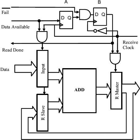
To show how recovery can be achieved after a synchronization failure, we give a simple example in Figure 7.19. Here input data from the sender is normally clocked into the input register, and then added to the R register which has a slave refreshed whenever the input register is overwritten. Read done is signalled back to the synchronizer during the next cycle by the flip-flop B which is clocked by a delayed read clock sufficiently far before the following cycle to enable the read pointer to be updated.
We will assume that the speculative synchronizer uses one read clock cycle for resolution of metastability between The Q-flop and flip-flops #3 and #4. The data available signal appears at the end of the first half of the cycle, and the fail signal does not arrive until after the end of the second half of the read cycle. The receive clock is timed to occur just after midway in the read clock.
If there is a failure of synchronisation such that the speculative data available signal is still metastable at the receive clock time, the input register, the slave, and the flip-flop A may all be corrupted. At the end of the second half of the read clock cycle and when the inverse receive clock occurs, the fail signal will force the flip-flop B to be set to 0, and the R register master will not be altered by the subsequent Receive Clock. Since the Read Done is not generated, the read pointer is not updated, and the data available is effectively allowed another cycle to settle before both the input and R register slave are refreshed.
Figure 7.19 Example of failure recovery.
In this scheme only one extra cycle is required every time a synchronization failure occurs, and provided the rate of writing is slower than the rate of reading this extra delay will rapidly be made up. Average latency is now 0–1 read clock cycle for the time between movement of the write pointer which may alter the state of the Empty signal, and the next read clock cycle, plus a half-cycle for synchronization plus 1 in 20 000 000 cycles for possible failures.
This is a relatively simple example, but in general, the strategy is to stop a pipeline when the failure is detected, and recompute or refresh corrupted values. It is important here to ensure that corrupted data, or control states are always recoverable, but this does not usually present a problem. This is similar to schemes in which a fast, but unreliable computation path may need to be backed up by a slower, but reliable one [44]. An alternative recovery scheme involves a shadow register for every data register in the receiving processor [66]. When an error is detected the shadow register is later loaded with the correct value, and a pipeline error is signalled. The processor pipeline can then be flushed and the incorrect data overwritten from the shadow register.
7.6 ASYNCHRONOUS COMMUNICATION MECHANISMS (ACM)
Communication between two asynchronous timing domains usually assumes that every data item sent by the writer to the reader by a channel must be read once and once only by the reader. This is not necessarily the case. There are situations where data may be generated, in the writer, and made available to reader, but not read, for example, a real time clock. The time is a global variable that may be required in one processor in one part of an algorithm, but if its value changes, it is not necessarily needed and the reader cannot be held up waiting for new data. Another situation which differs from the classical interpretation of a channel, is that of a signal from a sensor, where the writer (the sensor) cannot be held up, it must always be allowed to move on to the next reading of the position, temperature, of whatever is being measured even if the data item has not been read. The reader, on the other hand must take note of the value the sensor is producing at a particular point in the control algorithm, and if there is no value it must be held up. A classification of these different communication methods, known as asynchronous communication mechanisms (ACMs) [45–47], is shown in Table 7.2.
In a channel, both the reader and the writer can be held up, and all the previous synchronizers in this chapter are of this type. The pool ACM, allows a real-time clock to write new data items into a shared memory space, overwriting previous values no matter whether they have been read or not, neither the reader nor the writer can be held up. Signal data requires the writer to move on irrespective of the reader situation, but the reader must note new events.
Table 7.2 Classification of ACMs.
Figure 7.20 Passing data via an ACM with shared memory.
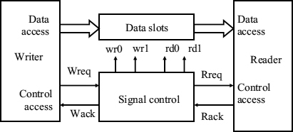
When the writer and reader processes are not synchronized, some kind of intermediate data repository, usually in the form of shared memory, is needed between them to facilitate the data passage. Typically this takes the form of a FIFO as in Section 7.2, but more generally the reader and the writer are separated by an ACM with some internal memory shared by both reader and writer as in Figure 7.20.
The objective of the ACM is to allow reader and writer to be as far as is possible asynchronous with respect to each other while maintaining the requirements of the data to be transferred. Since the writer may be continually writing to the shared memory, locations can be updated just as the reader if accessing the write location. In the FIFO this is avoided by preventing the read and write pointers from ever meeting. This requires some form of flow control in which the writer is not entirely independent of the reader, and the resulting wide pointer separations can lead to long latencies, when there are many more recent items in the memory than the one being accessed by the reader.
Important requirements of an ACM are data coherence in which any item of data that is being read from the shared memory must not be changed by the writer (i.e. no writing or reading in part), and data freshness where a read access must obtain the data item designated as the most recently written unread item, i.e. the data item made available by the latest completed write access.
The idea of coherence implies that there is mutual exclusion between write and read to the memory. In a software system this is usually provided by explicit critical sections where only one process can enter the critical section at a time. Using critical sections, however, may not be acceptable in real-time systems because the unpredictable waiting time makes it impossible to estimate the precise temporal characteristics of a process. It also makes the writer temporally dependent on the reader and/or vice versa.
This dependence may be in conflict with real-time requirements specified for the reader and/or the writer. For instance, in the Pathfinder mission to Mars, shared memory used for data communications was managed by a complex arrangement of critical sections, priorities and interrupts, but the long critical sections on the shared memory conflicted with the real-time requirements of subsystems, causing occasional system failures.
At this point, it is not necessary to say whether the ACM should be implemented as hardware, or software, and this is one of the strengths of the methodology. The system can be defined in terms of processes and ACMs of different types without committing it to a particular architecture. Only at a later date is it necessary to allocate processes to processors, and communication to hardware or software as the performance requirements of the system dictate.
An ACM is designed to avoid conflicts on data memory without resorting to explicit critical sections, but makes fundamental mode assumptions on the operations of the control variables. Mutual exclusion between writer and reader from the same location is achieved by the state of the shared memory control variables. In other words, the ACM shifts the problem of synchronization from the data memory to the control logic, which typically consists of small shared variables. The general scheme of a hardware ACM is shown in Figure 7.21. In this scheme access to a number of data slots is controlled by the shared variables and the signals wr0, wr1, rd0, rd1, etc. represent actions on those variables. Since read actions rd0, rd1 etc are initiated by the reader and write actions wr0, wr1, etc by the writer sometimes on the same variables at any time, it is possible that two or more actions may conflict. Because of this conflict the flip-flop holding a state variable can become metastable, and any assumption that that the variable always has a digital value does not hold. In practice a hardware ACM is often used by processes where the time between successive write and read operations is very long compared with the metastability resolution time constant, so that the values used are stable enough for each atomic action. The final state of a metastable variable may be true or false, so a robust ACM control algorithm must assume that the variable can settle either way.
Figure 7.21 ACM with control variables.
7.6.1 Slot Mechanisms
If only one data slot is used for both reading and writing, it will be impossible to make the writer and reader both asynchronous and keep the data coherent because the write and read could occur at the same time to the same register. If two slots are used the system can be made both asynchronous and coherent, but at the expense of freshness, since the system can write to one slot at the same time as reading from the other, but a series of writes one immediately following on the other may lock the reader out of the most recently written data.
Three- and four-slot mechanisms can both preserve coherence and freshness, and here we describe algorithms for pool reference data since these are rather different from the channel message data which can be adequately served by a FIFO.
7.6.2 Three-slot Mechanism
In Simpson's three-slot algorithm [46], the writer algorithm uses three pointers to access three common data items. These are the new pointer, n, the last pointer l, and the read pointer r. Data is written to the location pointed to by n, that is, d[n], data is read from d[r], and l points to the last data item that was written. n is computed from the values of r and l so that it is always different to both of them. If r and l are different, say 1 and 2, n takes up the third value, 3. If r and l are the same, n takes up the next value, 2 if they are both 1, the value 3 if they are both 2, and 1 if they are both 3. To write a data item into the common memory there are three steps. First, the input is written to the next location, then the last pointer updated to point to this location, and finally the next pointer is reassigned to a fresh location different to both read and last. More formally the three steps are:
wr: d[n] := input
w0: l := n
w1: n := ¬(l, r)
To read, the read pointer is first updated to point to the last item written, and then the item is output as follows:
r0: r : = l
rd: output := d[r]
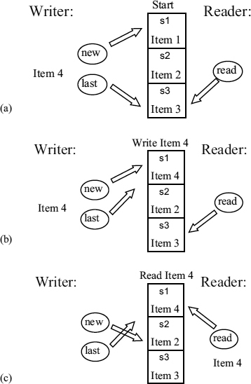
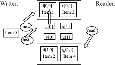
As an example Figure 7.22 shows a new data item (Item 4) being written.
In (a) l = 3, n = 1, and r = 3. This means that the last, and freshest item was written into slot number 3, and the input (Item 4) must be written into slot number 1, d[1]. Following the write, (b), l updated to 1 and n updated to 2. In this example we are going to assume that the reader makes an access as soon as item 4 is written. In that case, (c), r becomes 1, following the read and n is changed to 2. From this it can be seen that there is always a third slot for the next item, so that read and write can never clash (coherency), and the read pointer always points to the latest fully written item (freshness).
Figure 7.22 Writing a new item in a three-slot ACM.
7.6.3 Four-slot Mechanism
The algorithm of the four-slot mechanism is as follows
wr: d[n, ¬s [n]] := input
w0: s[n] := ¬s[n]
w1: l := n|| n := ¬r
r0: r := l
r1: υ := s
rd: output := d[r, υ[r]]
Here the writer and reader processes are single-thread loops with three statements each. The mechanism maintains the storage of four data slots d[0, 0] to d[1, 1] and the control variables n, l, r, s[0…1], and υ[0…1]. Variables n, l, and r are single bits indicating next, last and read location for the upper or the lower pair of slots, as shown in Figure 7.23. Individual slots can be addressed by s[0…1], and υ[0…1] which are vectors of two single bits. The statements wr and rd are the data accesses and the other statements are used by the writer and reader to choose slots and indicate such choices to the other side. The statement w1 is a parallel assignment.
In Figure 7.23 n = 0 points to the upper pair of slots, and l = 1, r = 1 point to the lower pair. s [0] = 1 and υ[0] = 1. There are four items already written into the slots, of which Item 4 is the freshest, and a new item (Item 5) is about to be written. The statement
Figure 7.23 Four-slot ACM.
wr: d[n, ¬s[n]] := input
writes it into the upper left hand slot, d[0, 0]. Statement
w0: s[n] := ¬s[n]
changes s[0] from 1 to 0, and
w1: l := n|| n := ¬ r
makes l = 0, and n = 0, thus the next item to be written would go into d[0,1]. A read updates r to 0, and υ[0] to 0 so that the next read comes from d[0,0],which is the freshest item. Successive writes without a read intervening will go to alternating slots in the same pair (upper or lower) until the value of n changes, and this does not happen unless r changes. Successive reads without an intervening write cannot alter l, n or s, so are always read from the same location. Because n := ¬r after a write the next write is always to a different pair from the next read (coherency) and because the read is always from the same location as the last complete write, we have freshness.
The most important properties of these ACMs are potential full asynchronism, data coherence, and data freshness. The algorithms do not specify the relative timing relationship between the reader and writer processes. This implies that they may be allowed to operate entirely independently in time. The control variable l in both cases is used to steer the reader to the slot which the latest wr statement visited.
The one relative timing specification implied in both algorithms is that within the reader and writer processes, the statements must be executed in the order specified and any statement may not start without the previous one having completed, that is, they are atomic. The four-slot ACM has been shown to maintain full data coherence and data freshness when the ACM is operating in fully asynchronous mode and when the metastability assumptions about the writer and reader statements hold. This is true even when the individual statements are assumed to be globally nonatomic, i.e. including such extreme cases as any writer statement taking as long as an infinite number of reader cycles to complete. The three-slot ACM has been shown to maintain full data coherence and data freshness, but only if statement r0 is assumed to be atomic in relation to statements w0 and w1.
7.6.4 Hardware Design and Metastability
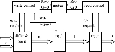
The four-slot ACM design provides maximum safety by adhering to the sequential specifications of the algorithm. However, one of the main arguments for a hardware solution compared with a software implementation is the potential of maximizing the speed of the ACM. This is the aim of the three-slot ACM implementation in Figure 7.24. Since it is known that the three-slot algorithm provides data coherence and data freshness if r0 is regarded as atomic relative to w0 and w1, we must use an arbiter to contain metastability, and this has the side effect of providing this atomicity. Each of register blocks in this figure has correspondence with one of the variables, so we can deduce that since the hardware solution of the three-slot ACM has similar form to the algorithm itself, and will have the correct behaviour.
In the three-slot algorithm, w1 changes n, w0 changes l, and r0 changes r. We must ensure that there is mutual exclusion between statement r0 and the statement sequence w0 + w1. This is done by a MUTEX which grants access to the registers either to the read control or to the write control, but not to both at the same time. Any metastability is contained within this MUTEX circuit. The block which implements the statement w1: n := ¬(l, r) ensures that the control variable n is assigned a value different from the current values of both l and r. In practice, this can be done in hardware by a look up table implementing the matrix ¬(l, r) = ((2,3,2), (3,3,1), (2,1,1)).
Figure 7.24 Self-timed design outline for a three-slot ACM.
7.7 SOME COMMON SYNCHRONIZER DESIGN ISSUES
Synchronizers are often omitted where they are needed in a system, and sometimes new synchronization circuits are invented which seem to eliminate, or avoid the problem of metastability [48]. These problems are common, but it is not easy to check a design for metastability. First it is necessary to find the conditions that might cause a circuit to go metastable, and then to demonstrate that it actually can be metastable. Metastability does not show in digital simulation, and might not even show up in simulation at the SPICE level because it depends on very small time differences, so special tools are often used to check for asynchrony. Unfortunately they are not perfect. Often they depend on the tool recognizing where clocks are independently timed, information which may not be available in the circuit description without special user input. Any signal whose time reference originates in one processor, and is to be used in another time frame is a potential cause of metastability and usually needs synchronization. Other causes of problems are circuits specially designed to detect metastability, take corrective action, and thus avoid the consequence of long time delays and/or unreliability. These must always be regarded with suspicion. Detecting metastability may itself require a decision, is the circuit metastable or not? And if it does, then the time to make that decision may also be unbounded.
Synchronizers made up of many parallel flip-flops have also been proposed [49]. Some designs can give an advantage, others may not, but generally the advantage is small, and the power required to support a multiple flip-flop synchronizer might be better spent in improving the gain bandwidth product of the flip-flop itself.
7.7.1 Unsynchronized Paths
All designs should be carefully screened to check for signals passing between independently clocked domains. In a safe system all of these should be synchronized.
7.7.1.1 No acknowledge
A common source of an unsynchronized signal occurs in a data transfer where the availability of data is signalled by a request from the sender accompanied by data. Most designers recognize that the request has to be synchronized to the receive clock before the data can be admitted, but sometimes it is forgotten that any acknowledge signal sent back from the receiver to the sender must also be synchronized. This is shown in Figure 7.25, where the acknowledge is asynchronous as far as the sender is concerned and must be synchronized to the sender clock.
7.7.1.2 Unsynchronized reset back edge
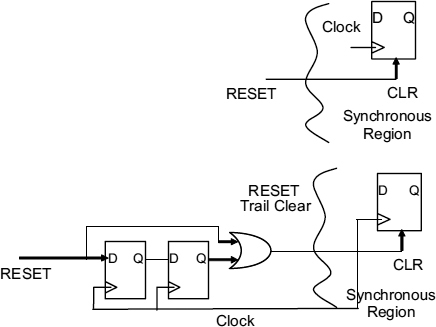
Another problem can be caused by an unsynchronized global reset. Why should this be a problem? The purpose of the global reset is to set all flip-flops in a system to a defined state, and the clear or preset inputs used to do this override any clock inputs so that the system will be put into the correct state irrespective of any clock activity. But when the reset signal finishes, however, it may be that the D input to a flip-flop resulting from some previous stage is high, where the low reset has forced the Q output low. Now as the reset trailing edge can occur at any time, when it returns high metastability may occur because the clock happens at about the same time.
Thus, the leading edge of the reset does not need to be synchronized, but the trailing edge does. A trailing edge synchronizer is shown in Figure 7.26 where the clear cannot return high until after the clock edge.
These are just two examples of unsynchronized sneak paths which may cause problems and are not easy to detect.
Figure 7.25 Unsynchronized acknowledge.
Figure 7.26 Asynchronous reset, and synchronized trailing edge reset.
7.7.2 Moving Metastability Out of Sight
Innovative designers, convinced that metastability is an avoidable problem in their design, have in the past produced ideas to eliminate it, or at least to avoid its consequences. These are not usually safe, and just end up moving the place where metastability occurs.
7.7.2.1 Disturbing a metastable latch
At the circuit level, it is clear that a metastable state is very sensitive to disturbance, and so a small externally applied stimulus could easily knock a metastable flip-flop out of its state and cause it quickly to resolve to a stable high or low. Typical of such ideas is Figure 7.27 which is an attempt to speed up metastability resolution.
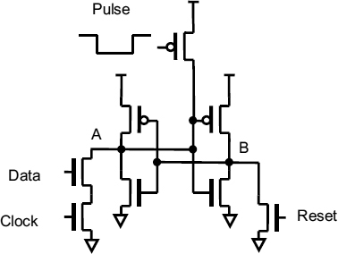
How it is supposed to work The latch in this Figure consists of two cross-coupled inverters, a clocked data input and a reset. An additional relatively small transistor has been put in to disturb the latch and help it resolve to predefined state if it ever becomes metastable. There are two possible variations of this scheme. First, the idea may be to apply the pulse unconditionally whenever the latch is clocked. In this case, if the data changes just as the clock goes low the latch is left in a metastable state. The additional p-type transistor is always pulsed on at this time so that node A is pulled up by a small amount at first, and then rapidly moves high, under the influence of the feedback loop.
Figure 7.27 Disturbing a metastable circuit.
Why it doesn't work The problem here is that without the extra transistor the latch is perfectly symmetrical, so that metastability occurs when the data goes high just a little before the clock goes low. With the extra pulsed transistor added node A is pulled up when the pulse occurs, but if the data change was a little earlier, node A would already have started to move down, and could actually be pulled back up to metastability by the pulse. The data can always change at a time which gets the circuit into metastability with any reasonable pull-up transistor. Only if the extra transistor is very large will node A always get pulled up quickly. But if it always gets pulled up, node A always ends up high. That could be achieved by connecting it straight to Vdd, and no decision is being made.
7.7.2.2 The second chance
The second scheme is to arrange the pulse to only come on when the circuit is metastable, so that fast decisions are left alone, and only the slow ones are disturbed.
How it is supposed to work Metastability is first detected, and then resolved by the pulse, so the circuit always works in a limited amount of time.
Why it doesn't work Again, the extra pulsed transistor causes node A to be pulled up when it is at a metastable level. Similarly if the data change was a little earlier, node A might have started to move down, and could be pulled back up to metastability by the pulse. Exactly where this new metastable point is depends on the circuit used to detect metastability. It is possible to imagine a metastability detector which gives a half output when node A is almost at the metastable level, and so half turns on the extra transistor. No matter how the circuit is designed, it is always possible to find input conditions halfway between those that give a final high outcome on node A and those that give a final low outcome.
One form of this circuit that does give an advantage is described in Section 3.7. It has two extra transistors, one on each node. Metastability still happens, but the circuit has an improved τ, not because metastability is disturbed, but because the loop mutual conductance is increased when the circuit is metastable by the extra current in the latch transistors
7.7.2.3 Metastability blocker
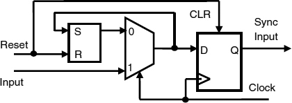
If metastability cannot be prevented from occurring, and cannot be eliminated in bounded time, perhaps its effects can be blocked from the following system. The circuit of Figure 7.28 is supposed to prevent metastability from affecting the synchronized input of a processor core.
How it is supposed to work First Reset clears both the latch and the synchronizing flip-flop. When the clock goes high, the input is selected by the multiplexer, and the SR latch is set. When the clock goes low, the latched input is selected by the multiplexer, and a clean signal clocked into the flip-flop next time the clock goes high.
Why it doesn't work The metastability has been moved from the flip-flop to the latch. Input and clock are still asynchronous, and if the clock goes low at around the time the input goes high, a short pulse could put the latch into metastability. Now there is a half cycle delay before the latch metastable level is clocked into the flip-flop, so the reliability is worse than the normal synchronizer. In this design, there is an even worse problem. It is possible for the input to go high just before the clock goes high. Now there is a short pulse on the D input to the flip-flop, which may or may cause metastability in that as well.
Figure 7.28 Metastability blocker.
7.7.3 Multiple Synchronizer Flops
Some synchronizer ideas are based on using many synchronizers in parallel to get some speed advantage, or eliminating the time overheads of synchronizing the control flow signals.
7.7.3.1 The data synchronizer
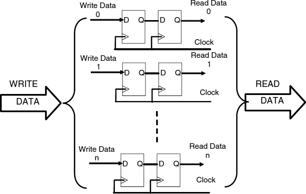
Synchronizers are usually placed in the data available and acknowledge paths. The data available signal cannot go high until the data is stable, and following synchronization, the synchronized data available signal is used to clock the data into an input register. Why not save time by using two flip-flops in every data bit path?
How it is supposed to work The read clock in Figure 7.29 samples every data bit when the clock goes high. There is then a one-clock cycle delay to resolve possible metastability between the first and second flip-flop in the data path. This second flip-flop then acts as the input register, so extra time to clock the input register is avoided, and latency improved.
Why it doesn't work Small differences in delay between each of the data bits will mean that some bits get correctly set, and others don't if the clock edge occurs at around the time all the data bits change. The data clock into the input register is then incoherent, some bits being left at their previous value and some set to the new value.
7.7.3.2 The redundant synchronizer
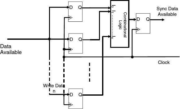
Another interesting idea is the redundant synchronizer, in which many flip-flops are clocked, and the probability of some combination of all the flip-flop outputs remaining metastable after a time t can be made vanishingly small if the number of flip-flops is large enough [49].
Figure 7.29 Data synchronizer.
How it is supposed to work In Figure 7.30 the input data available is clocked into many flip-flops simultaneously, and then a combinational logic block is used to compute some simple function of all their outputs. When the clock and data coincide, each of the flip-flops may resolve to a high, or a low level, or may remain metastable with a probability of P(M) = e−t/τ which decreases with time. Assuming that the data and clock edges of all the flip-flops are close to the balance point, the probability of the ith flip-flop resolving to a high after a time t is:
Figure 7.30 Redundant synchronizer.
![]()
The probability of is resolving to a low is:
![]()
and the probability of it being metastable is: Pi(M)
Now let us suppose that the function in the combinational logic block is AND, which appears to be the best choice.
Using p1 for the average probability of a flip-flop resolving to a high, and pM for the probability of it still being metastable, it is argued that with n flip-flops the probability of the output of an n-input AND gate still being metastable is:
(p1 + pM)n − p1n
As n increases this is a monotonically decreasing function, so if n is big enough it will eventually become very small. This means we can reduce the probability of metastability to an arbitrarily low level.
Why it doesn't work It is indeed true that the probability of metastability is much less as n increases if we only look at the case where the data available change is exactly at the balance point where the probability of flip-flop low outcome is equal to the probability of a high outcome. In a real system the probability of a data input changing at any specific time is just the same as the probability of it changing at exactly the balance point so we must consider, what happens if a data available input happens slightly earlier than the balance point. Now the probability of a high flip-flop is increased, and though the probability of metastability is reduced, it is only reduced by a small amount.
Sections 4.2 and 5.2 show that typically the distribution of metastable events with time shift is normal, and the probability of a high output will increase as the data time becomes earlier according to the cumulative distribution. Using this fact we can compare a synchronizer with one flip-flop and a one-input AND function, which is, of course the normal synchronizer with a two-flip-flop solution with a two-input AND gate.
Putting n = 1 we get the probability of metastability to be pM as expected, this is the normal synchronizer reliability, but putting n = 2 we get 2p1 pM + pM2. Thus moving the input a few picoseconds earlier we can increase the probability of high outputs from the two flip-flops at the same time by quite a lot as well as reducing the probability of metastability by a little. Suppose the input is earlier by about 0.8σ, where σ is the standard deviation of the timing jitter distribution (normally about 5 ps). This increases p1 from 0.5 to about 0.79, and reduces pM by a factor of 1.377. The net result is that probability of metastability, 2p1 pM + pM2, is a factor of 1.674 higher than before, so two flip-flops are worse than one. Maybe more might be better.
By shifting the data early enough we can increased the probability of high outcomes to such an extent that the most likely pattern in an n-flip-flop synchronizer is n − 1 highs, and one metastable output, leading to a high probability of a metastable AND gate output. The probability of metastability in any one flip-flop is significantly reduced, but the probability of metastability in the AND output is approximately n.p1n − 1 pM. Here there are n cases where one input is metastable, and the other n − 1 other inputs all need to be high. In order to get probability of metstability better than the one-flip-flop case we need to move the input by 1.39σ, so that pM drops to 0.5 of its original value, and p1 rises to 0.917. This cannot be achieved unless n > 31, so the AND gate needs 32 inputs. Beyond 32 there is a theoretical gain in reliability over the simple synchronizer. On the other hand there is an extra delay in the 32 input and gate which effectively reduces the synchronizer resolving time, and the strong possibility that a flip-flop that becomes metastable with an input offset greater than the standard deviation is likely to have a fabrication defect, and therefore to be slow.

