2
Modelling Metastability
Asynchronous data originating from outside a clocked system has to be synchronized to the clock before it can be used. This usually involves a choice made on the basis of the arrival time of the data, which is a continuous variable, and the result of the decision, which clock edge to use, is discrete. In this situation it is possible to have very small input time differences between the data available signal and the clock. Such choices are difficult as the input energy to the synchronizer circuit falls towards zero when the time difference becomes small, and the response time of the circuit then approaches infinity. In fact there is always a point at which the synchronizer time response can become longer than the available time, and the synchronizer circuit fails because its output has not reached a stable state [4,5].
Asynchronous systems have a similar problem where the system must decide which of two or more asynchronous requests for a common processing resource is to be granted first. In this case the circuit that makes the decision is called an arbiter, and the input energy to the arbiter is also derived from the time differences between the inputs. Again, this time difference is a continuous variable and can also approach zero, with the result that the arbitration time can approach infinity [5,6]. In both cases the decision element, usually a flip-flop, has become metastable, and the resolution time of metastability in a flip-flop is important to the reliability of the system.
2.1 THE SYNCHRONIZER
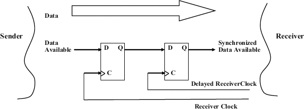
Most commonly metastability is seen in synchronization of data passing from one time domain into another. If the receiving domain is clocked, but the data input comes from a sending zone which may be clocked, but whose timing is unrelated to the receiver clock, we must first synchronize the data available signal to the receiving clock before any processing can be done. Typical synchronizer circuits use two edge-triggered flip-flops clocked by the receiving clock to achieve synchronization, as shown in Figure 2.1 with a time delay between the clocking of the first and second flip-flops.
The time delay is there to allow metastable levels in the first flip-flop to resolve before the second flip-flop is clocked, and therefore has a strong impact on the reliability of the synchronizer. The longer the flip-flop is given to resolve metastability the less likely it is that the synchronizer will fail. A flip-flop normally has two stable states, but the transition time between them is only guaranteed if the inputs conform to the set-up and hold times between data and clock. In the synchronizer the set-up and hold conditions will often be violated because the data available and clock timing are unrelated, so in a typical situation any value of time difference between them is possible. When the data input changes at a time close to the clock edge, the circuit outputs can be left in a metastable state, and the synchronizer designer needs to know how much time to allow in order to keep the chance of failure to an acceptable level
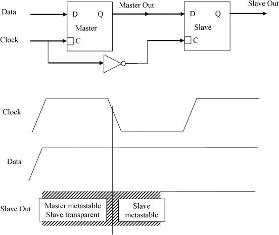
The edge-triggered flip-flops in the synchronizer are usually made from two level triggered latches in a master slave arrangement as shown in Figure 2.2. When the clock level is low, the master is transparent, that is, its data input is copied to the master output, but the slave is opaque and holds the previous value of the data input. When the clock goes high, the master becomes opaque, and the slave transparent. Because the clock and data times are unrelated in a synchronizer the set-up and hold times of the master latch are frequently violated. The master output may then go into a metastable state, and it may take some time to resolve to a well-defined digital level. While the clock is still high, any metastable level at the master output will also violate the conditions for the slave to act digitally and metastability can appear on the slave output. Since the problem is caused by master metastability the synchronization time will depend only on the metastability resolution time of the master. If the clock goes low before metastability is resolved in the master, the slave clock goes high at the same time and so the slave may now be metastable. From this point onwards any additional resolution time required depends on the characteristics of the slave.
Figure 2.1 Synchronizer.
Figure 2.2 Edge-triggered flip-flop made from two latches.
To determine what these characteristics are, we need to examine what happens when the individual master and slave latch circuits become metastable.
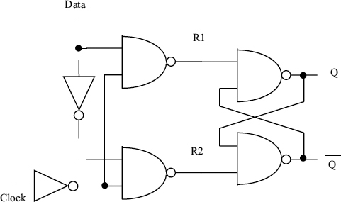
Figure 2.3 D latch.
A very simple design for a latch is shown in Figure 2.3. When the clock is high, both R1 and R2 are high, and the latch is opaque, that is, it is not affected by the data input and simply retains its previous state. When the clock goes low, R2 follows the data input, and R1 is the inverse of the data input. If the data input is high, R2 must be high, and Q is high. If the data input is low R1 is high, R2 low, and Q becomes high.
There are two ways that the circuit can become metastable, either the inputs are not digital levels, or the timing conditions are not observed. In the synchronizer circuit it the data can go high just before the clock goes high, so in this circuit there may be a runt pulse on R1, followed by both R1 and R2 going high. At this time the latch output Q may not yet have reached a high state, but the input from the D input is now inactive and only the cross-coupled feedback inputs can determine whether it ends up high or low.
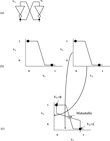
Since R1 and R2 are now high, they take no further part in determining Q, so what happens then can be illustrated by considering a simple latch circuit made from two inverters.
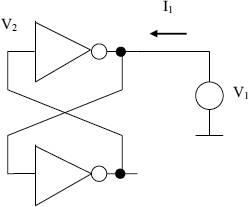
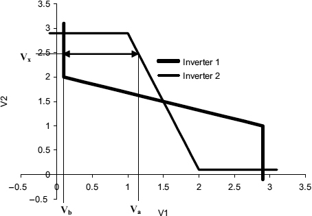
This is shown in Figure 2.4(a). Here the input to the inverter on the left is the same as the output of the one on the right V2, and the input of the right hand one is the output of the left hand one V1. When the latch is metastable input and output voltages which are not just high or low can appear at the two points which are both inputs and outputs to the inverters. We can plot how the the output changes against the input for each inverter on different graphs, (b), or we can plot them both on the same graph by flipping the right-hand graph over and superimposing it on the line for the inverter on the left (c), so that only points, which lie on both input/output characteristics, are possible for both inverters in the long term.
One point has V1 = 0 and V2 = 1, and another has V1 = 1 and V2 = 0. These points are the two normal stable states. There is also a third point where V1 = V2 = 1/2, which is the metastable state.
Figure 2.4 Metastability: (a) Latch bistable; (b) Static characteristics of inverters; (c) Superimposed characteristics.
Figure 2.5 Output current against voltage.
To see this, suppose that the voltage V1 is held by a voltage source, and then slowly increased from zero to Vdd as in Figure 2.5.
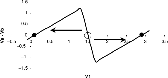
Suppose V1 is held by the voltage source at a value of Va volts. Because its input is at Va, the output of the lower inverter in Figure 2.5 is at Vx. Vx at the input of the upper inverter would normally produce Vb at its output, but since it is held at a different voltage, Va, a current is drawn from the voltage source, which is proportional to Va − Vb. Now let's change the voltage V1 slowly from zero to Vdd. The current first increases, as the difference between Va and Vb increases, and then decreases to zero at the central point. Beyond that point, current has to be pulled out of the of the upper inverter to hold its output down, and this current only drops to zero at the second stable point where V1 is high. The two superimposed characteristics are shown in Figure 2.6, and the resulting plot of Va − Vb, which is a measure of the current, against V1 is shown in Figure 2.7.
Figure 2.6 Superimposed characteristics.
Figure 2.7 Va − Vb drive for different values of V1.
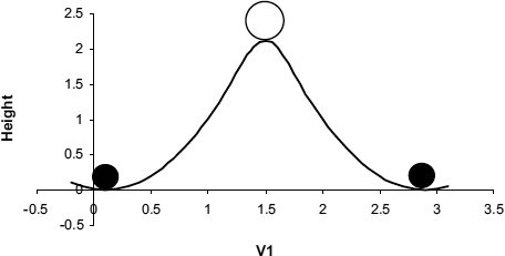
In a real circuit there is always some stray capacitance associated with each node, so with a capacitor connected to the output rather than a voltage source, we can see what will happen when the node is metastable. In Figure 2.7 the capacitor is discharged when V1 is on the left-hand side of the central point, pulling V1 lower, and charged if it is on the right-hand side, pulling it higher. The central point is not stable. This kind of instability is analogous to a ball placed on top of a hill (Figure 2.8) if we make the slope of the hill the same as Figure 2.7, i.e. positive on the left-hand side and negative on the right-hand side, there are two stable points where the slope is zero, on either side of the central, unstable point where the slope is also zero. When the ball is let go it will eventually roll down to one side or the other, but with careful placement it can stay in the metastable state at the top for some time.
The analogy of Figure 2.8 shows that the output moves rapidly to either the V1 = 1 and V2 = 0 state or the V1 = 0 and V2 = 1 state, the differences between the actual operating trajectory and the static characteristics being accounted for by the output capacitance which absorbs the difference current. The smaller the capacitance, the faster it goes. The central point is usually called the metastable point, and a latch is said to be metastable if it is in balance between a 1 and a 0, with the drive towards the two stable points, called attractors, close to equal. The difficulty with metastability is that with a net drive of zero, the capacitances are neither charged, nor discharged, and the circuit can remain at the metastable point for a long time, much longer than its normal response time with digital inputs.
Figure 2.8 The ball on the hill.
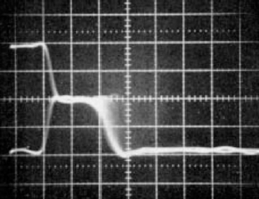
If the input clock/data overlap is very close to a critical point, metastability can be reached from either stable state as shown in Figure 2.9. This particular photograph was taken by selecting all the metastable events in a level triggered latch, which lasted longer than 10 ns (two divisions) [6]. Several traces are superimposed, with outputs starting from both high and low values, then reaching a metastable value about halfway between high and low, and finally going to a stable low level. It can be seen that the traces become fainter to the right, showing that there are some with long metastability times, but fewer than the short metastability time responses.
If only one flip-flop is used for synchronization, the master latch in the flip-flop will often be left in a metastable state and a long time may elapse before its output escapes to a stable high or low. A half level input, or a change in level as the clock changes in the slave may then result in a long time delay in the output data available signal which is first read by following circuits as a low level, and then later as high.
Figure 2.9 Output from a metastable latch.
Figure 2.10 Synchronizer output times.
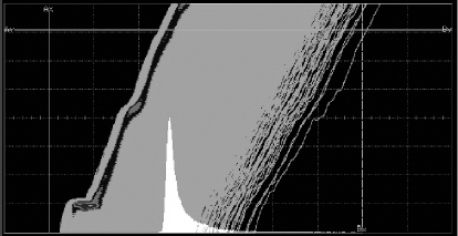
Figure 2.10 shows the output of a CMOS flip-flop used in a synchronizer situation. Many outputs have been captured on a digital oscilloscope at 1 ns/division, and though the circuit is specified to have a response time of around 3 ns some of the high-going outputs are 5 ns or more after the clock time. As time increases from left to right, the density of the traces reduces, because the probability of the output changing reduces. A histogram of the number of outputs changing at a particular time is also shown in this figure (the white area, in which the height at a particular time is proportional to the number of outputs crossing the Ax line at that time). If the output changes late, there may be synchronizer failures, but the longer the delay allowed, the less likely is the synchronizer to fail by indecision. We can explain metastability qualitatively this way, but to produce reliable designs a more accurate quantified model is needed.
2.2 LATCH MODEL
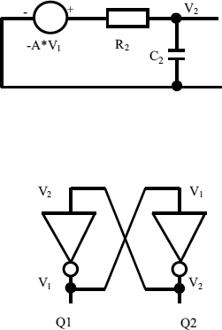
In the metastable state both inverters making up the flip-flop are operating in a linear mode. If they were not, the circuit would never escape from metastability, and to compute its escape time it is necessary to analyse the analog response of the basic circuits used. Most models of flip-flop circuits operating as synchronizers assume that the cross-coupled gate circuits making up the flip-flop are in a small signal mode, never far from the metastable state. Here to make the analysis simpler by eliminating constants, we will assume that the metastable state of the gates is at 0 V, rather than Vdd/2. This means that a digital high output is + Vdd/2, and a low output is − Vdd/2.
Figure 2.11 Small signal models of gate and flip-flop. Reproduced from Figure 13, “Synchronization Circuit Performance” by D.J. Kinniment, A Bystrov, A.V. Yakovlev, published in IEEE Journal of Solid-State Circuits, 37(2), pp. 202–209 © 2002 IEEE.
The gates can now be modelled as two linear amplifiers [6–8]. Each gate is represented by an amplifier of gain −A and time constant CR, as shown in Figure 2.11. Differing time constants due to different loading conditions can also be taken into account [8].
The small signal model for each gate has a gain −A and its output time constant is determined by C/G, where G is the gate output conductance and is equal to 1/R. In a synchronizer, both the data and clock timing may change within a very short time, but no further changes will occur for a full clock period, so we can also assume that the input is monotonic, and the response is unaffected by input changes.
For each inverter we can write:
The two time constants can be simplified to:
This is a second-order differential equation, and has a solution of the form:
In most practical cases, the inverters have a high gain, and are identical, so A >> 1, ![]() .
.
Both Ka and Kb are determined by the initial conditions, τa and τb by τ1, τ2, and A. Typical values of τ1, τ2, and A for a, 0.18 μ, process, are 35 ps for τ1 and τ2 (depending on the loading of the inverters) and 20 for A. Usually the values of τ1 and τ2 are similar to those of an inverter with a fan-out of 4, since both times are determined by the capacitances, conductances, and gain of the transistors in the circuits.
This model is valid within the linear region of about 50 mV either side of the metastable point. Outside this region the gain falls to less than 1 at a few hundred mV, but the output resistance of the inverter and the load capacitance also drop significantly, R by a factor of more than 10, and C by a factor of about 2. Thus, even well away from the metastable point the values of τ1 and τ2 still have values similar to those at the metastable point.
2.3 FAILURE RATES
Using the model of metastability above, it is possible to estimate the input conditions necessary to produce a metastable response of a given time, and hence how often this time will be exceeded in a synchronizer. If we assume that we are only interested in metastable events that take a much longer time than the normal flip-flop response time, we can neglect the first term in Equation (2.4) for the output voltage and use:
The initial condition Kb depends on the input time overlap between clock and data. If the data input changes to a high much earlier than the clock, Kb will be positive, so the output voltage will reach the digital high value of + Vdd/2 quickly. If it changes from low to high much later than the clock Kb will be negative, so the output voltage will reach a low value quickly. In between, the value of Kb will vary according to the relative clock data timing, and at some critical point Kb = 0, so the output voltage is stuck at zero. We will call the clock data timing that gives Kb = 0, the balance point, where in the previous analogy, the ball is exactly balanced on top of the hill and we will measure input times relative to this point using the symbol Δtin. The value of Kb is given by:
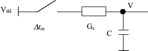
where θ is a circuit constant which determines the rate at which the clock data overlap converts into a voltage difference between the two nodes. If the cross coupled gates in the flip-flop are 2 input NAND gates either Vdd, or 0 V, and are connected via a conductance Gs to the output capacitor C for a time Δtin as shown in Figure 2.12, the output node will charge or discharge, moving its voltage away from the central point Vdd/2. Gs is usually less than AG, and τs = C/Gs is similar to the rise or fall time of that gate, so θ≈ Vdd/2τs.
Metastability is over when the latch output has reached normal levels, either high or low. The time taken to reach |Ve|, the exit voltage where the trajectory leaves the linear region and can be regarded as a stable high, or low voltage, can be calculated from Equation (2.5) by putting V1 = Ve. Since Kb = θ Δ tin, this means that the exit time is given by:
If the timing relationship between data and clock changes is unknown, all values of Δtin are equally probable. In these circumstances It is usual to assume that the probability of any input smaller than given overlap, Δtin, is proportional to the size of the overlap, very small values being therefore much less common than large ones. This is usually true if the timing of both send and receive clocks are independent oscillators. When the sending data rate is, on average fd and the receiving clock frequency fc, each data item sent could occur at any time between 0 and 1/fc of the next receiving clock edge, so the probability of that data available signal having an overlap of Δtin or less, is fc Δtin.
Figure 2.12 Input time constant.
Within some long time T there will be fd T data items transmitted, so the probability of at least one of the overlaps being less than Δtin is fd fc T Δtin.
If the synchronizer fails when the input overlap is shorter than Δtin by giving an output response longer than the resolution time allowed, the mean time between failures will be:
Failure occurs when
![]()
so we can get the mean time between failures of the synchronizer as:
This is more usually written as
where Tw = Ve/θ, and Tw is known as the metastability window.
MTBF depends on fc and fd, which are system parameters rather than circuit parameters, so we can use Equations (2.8) and (2.10) to get a characterization of a synchronizer which is dependent only on the circuit parameters τ and Tw:
The metastability window is the input time interval for which output times are longer than normal. If 0 < Δtin < Tw, then the output response time to Ve, t, is greater than zero, and the circuit is metastable. Input time differences outside this range either cause a normal response or no change. The value of Tw is determined by the input time constant θ and the point at which the flip-flop exits from metastability Ve; thus, if
![]()
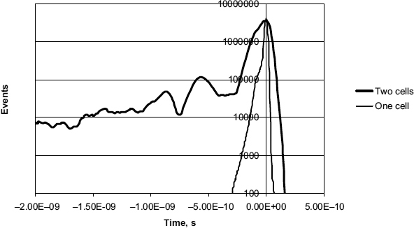
Tw is the same order of magnitude as the rise time of the gate. The value of τ is mainly determined by the feedback loop time constants, and since both Tw and τ are determined by channel conductances and gate capacitances, they are likely to be similar. This analysis applies to most simple latches, but may not hold for more complex devices, made from gates with more than one time constant in the feedback loop, or with long interconnections. It is very important for any flip-flop used for synchronization that it is characterized as a single cell with a fixed layout, and not assembled from individual gates or, for example, FPGA cells, because the feedback interconnection may have additional time constants, and the differential equation that describes the small signal beviour will be correspondingly complex. An example of multiple time constants is shown in Figure 2.13, where a latch has been assembled out of two FPGA cells. In this figure the latch output change is being used to trigger the oscilloscope, and the figure shows a histogram of clock events. The time scale is 0.5 ns/division. Because of the additional delay in the feedback loop the resolution time constant is nearly 1ns, and the histogram of clock to output times rises and falls as a result of oscillation in the output trajectory. For comparison the histogram from a standard latch on the same FPGA is also shown. Here, the resolution time constant is much faster at around 40 ps and there is no sign of oscillation.
Figure 2.13 Multiple FPGA cell latch.
If there is enough delay in the feedback loop, as is the case with latches constructed from more than one cell, the amplitude of the oscillation produced can be sufficient to take the gates outside the linear region, and the oscillation can look like a square wave, which persists for much longer than the times shown even in Figure 2.13.
If the time allowed for metastability is short, we must also take into account the first term in the response equation. For many metastable events, the initial conditions are such that Kb, which is the voltage difference between output nodes at the start, is less than 10 mV, and while Ka, the common offset at the start, may be as much as 0.5 V. In these circumstances the Ka term is important, but only in determining the response times for metstable events resolving early. This is because simple circuits using gates with only one time constant, always reach the linear region quickly. τa is small outside the linear region and so the Ka term becomes small very quickly. The metastable events that cause synchronizer failures last a long time, and will have trajectories that spend most of their time in the linear region and so we can usually still use the simplified second-order model to predict the time it takes flip-flop circuits to escape from metastability.
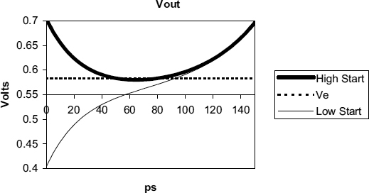
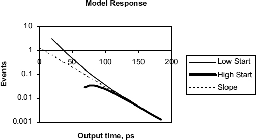
The difference between early and late trajectories, and how they are affected by the Ka term can be seen in Figure 2.14.
This figure shows the response of the two outputs in a latch against time as predicted by the small signal model when both outputs start from a point higher than the metastable level and from a point lower. There is a common mode initial offset of both outputs given by Ka = + 150 mV and − 150 mV from the metastable level of 0.55 V for the high start and low start curves respectively. For both these trajectories Kb = 4 mV, representing the initial difference between the two outputs. We use τa = 25 ps and τb = 42.5 ps to represent a typical situation where A is about 5–10.
Figure 2.14 Model response. Reproduced from Figure 2, “Synchronization Circuit Performance” by D.J. Kinniment, A Bystrov, A.V. Yakovlev, published in IEEE Journal of Solid-State Circuits, 37(2), pp. 202–209 © 2002 IEEE.
It is common for the exit from metastability to be detected by an inverter with a slightly different threshold from the metastability level of the flip-flop. Thus when Vout exceeds that level the inverter output changes from a high to a low. The metastability level of the flip-flop here is 0.55 V, and the threshold level is 0.58 V (the dotted line). Vout exceeds 0.58 V at 80 ps for the high start of 0.7 V and at 93 ps for the low start of 0.4 V. Note that the time difference depends upon the threshold level, and that if the high start trajectory never goes below 0.58 V, that is if Kb > 4.7 mV, metastability is not detectable for output time delays between 0 and 65 ps because the detecting inverter output remains low all the time. From these curves it can be seen that the metastability resolution time depends on the value of Ka during the first 100 ps, but not beyond that.
2.3.1 Event Histograms and MTBF
Measurements of flip-flop performance in metastability have been done in at least two different ways.
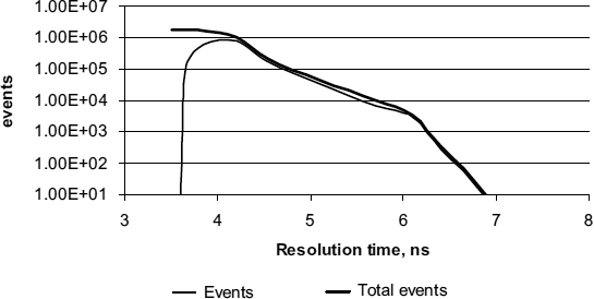
The most common measure is to count the number of times in a given period that metastability lasts longer than a particular time t. This is a measure of MTBF when the resolution time is t (Equation 2.10). If T is the time period over which the events are counted, MTBF = T/(total events) (Equation 2.12). A plot of the total events lasting longer than a particular resolution time for a synchronizer flip-flop is shown in Figure 2.15 where it is compared with the second measure.
The alternative is to count the number of times the output escapes from metastability within δt of t (events). Again T is the period over which events are measured, and the number of events that resolve within δt is

These events are also shown in Figure 2.15. Because the events scale is logarithmic, and many more events appear if the resolution time is only slightly reduced, the total events curve is only slightly above the events curve in most places. The main differences between the two sets of results are that small variations in the slope of the curve tend to be slightly exaggerated in the events curve, so that the change in slope shown in Figure 2.15 at around 6 ns appears to be sharper, and the two curves diverge for output times below the normal propagation time of the flip-flop.
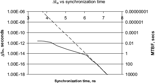
The same data can be presented in a more useful form (Figure 2.16) which shows the MTBF against resolution (synchronization) time as well as the input time required to give a particular resolution time. Using Equation (2.12) total events can be divided by the time T, during which the events were collected to give 1/MTBF, and (2.11) enables the value of Δ tin to be calculated. Graphs like this are also used to find the values of the circuit parameters τ, and Tw. If at any point we draw a tangent to the curve (shown by the dashed line in Figure 2.16) the slope of the tangent is −1/τ, so τ can be calculated. Here it is about 125 ps, and the intercept on the Δ tin axis is Tw. Tw can be measured at the normal propagation time, or at t = 0, in which case the value of Tw0. = 107 s here, but if it is measured from the normal propagation time of the flip-flop, about 3.9 ns, Tw = 3×10⁻⁷.
Figure 2.15 Events against resolution time.
Figure 2.16 MTBF, τ, and Tw.
The methods used to measure event histograms from typical circuits are described in more detail in Section 4.2.
Figure 2.17 shows how an initial offset affects the measurement of metastability. In Figure 2.17, Ka = + 150 mV for the high start curve, and −150 mV for the low start, both with τa = τb = 33 ps. This is a histogram of the probability of an output trajectory escaping metastability within 3.3 ps of a particular output time. In order to calculate the model responses in Figure 2.17 a uniform distribution of voltage offsets Kb has been derived from a distribution of input time differences by using the relationship between Kb and Δ tin given in Equation (2.6), where θ = 10 mV/ps in this case.
Figure 2.17 Events per unit time as a function of metastability time. Reproduced from Figure 3, “Synchronization Circuit Performance” by D.J. Kinniment, A Bystrov, A.V. Yakovlev, published in IEEE Journal of Solid-State Circuits, 37(2), pp. 202–209 © 2002 IEEE.
In a real experiment the number of events at a particular time is given by Equation (2.13). In Figure 2.17, τ = 33 ps, Tw = Ve/θ = 33 mV/10 mV/ps = 3.3 ps, and δt = 3.3 ps, so this figure shows the output event histogram against output time for the low start and the high start situations corresponding to the two values of Ka.
We use T = 3.3 ms, fc and fd = 30 MHz, to get a number of events (in this case a probability of a number of events if the number is less than one) of around 1 when t = 0, though in practice a time T of seconds would give many more events. The two curves deviate from the expected straight-line relationship, the high start curve recording no events before 65 ps because trajectories with large enough initial conditions do not intersect the output threshold of 0.58 V, and then events are recorded earlier than expected.
In the low start curve, events are delayed rather than accelerated by the effects of the Ka e−t/τa term in Equation (2.4), so the event histograms can look quite different at low values of t, though they converge for high values. This is important if we are going to use the slope of early events to predict MTBF values for much longer synchronization times, and we must use the full expression including Ka as well as Kb for calculating the mean time between synchronizer failures. Putting Vs for the initial common mode offset voltage Ve for the final voltage where the trajectory leaves the linear region, as before, we have:
Hence, by the same argument that we used earlier, we can show:
Now

and is no longer constant. In many circuits the initial offset is not negligible, and so the initial value of Tw can be different from its final value; either higher, or lower, depending on the polarity of the difference between Ve and Vs, and it is dangerous to use early values of slope to calculate τ
2.4 LATCHES AND FLIP-FLOPS
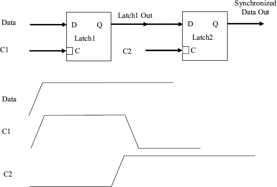
If a synchronizer is made from two latches, its reliability depends straightforwardly on the time allowed for the first latch to resolve between the rise time of the first and the second latch clocks C1 and C2 as in Figure 2.18. The MTBF calculation given by Equation (2.10) applies. The throughput of the two latch arrangement is limited, as the input data can only be sampled when C1 goes high, and C1 cannot be taken low until C2 goes high. The resolution time available for the latch1 output is then only half the cycle time.
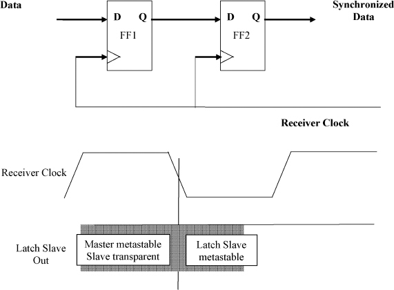
To increase the throughput, synchronizers are normally made from two edge-triggered flip-flops as shown in Figure 2.1. This allows a resolution time approximately equal to the cycle time, but calculation of the reliability is more complex. The reliability now depends on resolution of metastability in the master–slave combination, and the important factor is the probability of resolution before the end of the second half of the clock cycle, because that is when the synchronized output appears. In Figure 2.1 both FF1 and FF2 are made from two latches, and the output of FF1 can become metastable either as a result of metastability in the master of FF1 being copied through the slave in the first half of the clock cycle, or metastability in the slave being induced by set-up and hold condition being violated for the slave of FF1 when the clock goes low at the beginning the second half of the clock cycle. Slave metastability is usually caused by metastable events at the output of the master latch in FF1 that resolve very close to the falling edge of the clock. The number of such events within a time δt of the clock half-period t/2 is given by Equation (2.13), and is:
Figure 2.18 Latch-based synchronizer.
Any metastability must be resolved by the slave latch of FF1 in the second half of the cycle, within a time t/2, so according to Equation (2.11) only events within a time Δ tin of the balance point of the latch will cause failures where:
Putting Δ tin = δt in Equation (2.16) we get the number of events that cause the synchronizer fail in a long period of time T, which is:
From this we can compute the MTBF of the master slave combination:
The form of Equation (2.19) is exactly the same as Equation (2.10), but the value of Tw for the edge triggered flip-flop combination is ![]() , which is slightly different from the value of Tw for its component latches.
, which is slightly different from the value of Tw for its component latches.
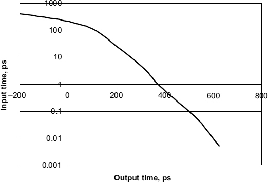
As well as having a different Tw the flip-flop has a different behaviour when the input is outside the metastability window. For inputs much earlier than the clock, a latch is transparent, so that the output follows the input with a short delay and the output time can go negative. On the other hand the output of an edge-triggered flip-flop does not change until after the clock edge, so no output events are seen with times earlier than the clock edge time.
Figure 2.19 Edge-triggered flop-flop-based synchronizer.
This analysis assumes that both latches are identical, and does not take into account factors like the propagation delay of signals through a transparent latch which will affect the proportion of the clock cycle available for metastability resolution.
Figure 2.20 Latch input time vs output time showing negative values for output time.
2.5 CLOCK BACK EDGE
Because of the internal construction of an edge-triggered flip-flop, there is often a significant increase in the failure rate in the second half of the clock cycle due to the delay in the slave latch of the flip-flop. We can now extend the theory presented so far to show what happens when the back edge of the clock occurs.
Consider two similar master and slave level triggered latch circuits cascaded to form a single edge-triggered circuit as shown in Figure 2.21.
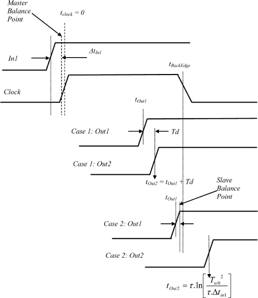
Here the master and slave can both be reset so that both Out1 and Out2 are low. When the clock is low, the master is transparent and any change in In1 is copied through to Out1 with a delay Td determined mainly by internal large signal gate delays. In normal operation In1 does not change within the set-up time before the clock rising edge, or inside the hold time after the rising edge, thus Out1 is steady when the master latch goes opaque and input changes no longer have any effect. At around the same time as the clock rising edge, the slave clock falls and so the slave goes transparent. Now the Out1 level is transferred to Out2 with a delay Td.
If the circuit is used as a synchronizer the input can go high at any time and so a rising edge on the input In1 which occurs just before the clock rising edge may cause the master to go into metastability. If the metastability is resolved well before the falling edge of the clock the change in Out1 is copied through the transparent slave to Out2 with the normal delay Td and if it is resolved after the falling edge the timing of Out2 is unaffected. Because the change in Out1 and consequently In2 may happen very close to the falling clock edge of the master, an input change can fall in the metastability window of the slave. Consequently there is a low, but finite probability that metastability in the master can produce metastability in the slave.
The two latch circuits are normally similar, so that the metastability time constant τ, in both is about the same and it is often assumed that the total resolution time of a metastable output, tOut2 follows the natural logarithmic form described in Equation (2.7).
Figure 2.21 Edge-triggered synchronizer.
Figure 2.22 Waveforms of master and slave in metastability.
In this equation Δ tin1 is the input time relative to the balance point. In fact, this relationship does not quite hold for an edge-triggered flip-flop, as the following analysis shows. In Figure 2.22 the waveforms of the master and slave are shown when both are close to metastability. In this figure the rising edge of the clock occurs at a time tclock = 0 and all times are measured with reference to this time. If the slave output occurs at a time, tOut1 late in the first half-cycle of the clock, its timing depends on the input time Δ tin1, before the balance point. The closer Δ tin1 is to the balance point of the master, the later is tOut1: We can plot Δ tin1 against tOut1 for the latch on its own by observing that
From this it is possible to find the output time of the slave tout2. There are two cases:
Case 1: tOut1 happens well before the back edge of the clock, so that the slave is transparent when its input changes. In this case the constant delay of the slave Td is simply added to t Out1, so t Out2 is given by:
Case 2: the slave may go metastable. In this case t Out1 must be very close to the absolute slave balance point time. We have already seen Equation (2.1) that in the second half of the cycle,

so using the relationship between MTBF and Δ tin in Equation (2.8) we can write
Here, the balance point has changed. In case 1, the balance point was the input that gave equal probability of a high and low outputs in the master, but in case 2, it is the point that gives equal probability of a high and low outputs in the slave. The balance point for the master–slave combination is therefore the input time that gives a slave input exactly at the balance point of the slave.
When compared with a latch, the balance point for the combination is shifted by this amount. Any plot of the input times against output times for a flip-flop made from two latches must therefore be measured from this new point. The change makes little difference for values of for values of t Out1 << tBackEdge, since
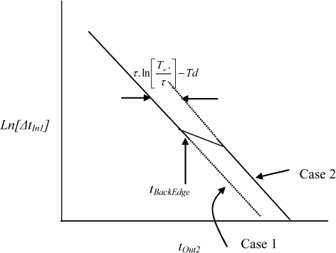
Figure 2.23 Case 1: slave transparent, case 2: slave metastable.
![]()
but it becomes important when t Out1 ≈ tBackEdge.
Figure 2.23 Illustrates the input time against output time that may be expected from a master–slave flip-flop. Case 1, on the left shows the relationship of Equation (2.22) with a slope of τ, normally seen between Δ tin1 and tOut2 when tOut2 < tBackEdge. On the right, the slope of the curve given by Equation (2.23) when tOut2 > tBackEdge remains the same, but there is a displacement which is given by the difference between the two cases:

or simplifying,
Here it can be seen that the offset depends on the circuit constants τ, T w0 and Td.
Synchronization and Arbitration in Digital Systems D. Kinniment
© 2007 John Wiley & Sons, Ltd

