
Chapter 4
Design Process
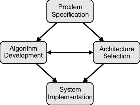
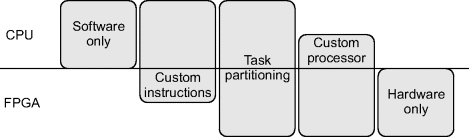
The process of developing an embedded image processing application involves four steps or stages (Gribbon et al., 2007). The relationship between these is illustrated in Figure 4.1. The problem specification clearly defines the problem in such a way that the success of the proposed solution can be measured. The algorithm development step determines the sequence of image processing operations required to transform the expected input image or images into the desired result. Architecture selection involves determining the computational structure of the processors that are required to execute the algorithm at both the application and operation levels. Finally, system implementation is the process of mapping the algorithm onto the selected architecture, including construction and testing of the final system.
Figure 4.1 The relationship between the four main steps of the design process.
It has been observed that the development of complex algorithms on FPGAs is sensitive to the quality of the implementation (Herbordt et al., 2007). To gain a significant speed improvement over a software implementation, it is necessary that a significant fraction of the algorithm can be parallelised. Often the speedup obtained from implementing an application on an FPGA is disappointing. One of the main factors is that it is not merely sufficient to port an algorithm from software onto an FPGA implementation. To obtain an effective and efficient solution, it is necessary for the computation and the computational architecture to be well matched. While algorithm development is usually considered part of the software engineering realm, the design of the processing architecture is firmly in the domain of hardware engineering. Consequently, FPGA-based image processing requires a mix of both skill sets. To fully exploit the resources available on an FPGA, the system implementation stage often requires changes to both the algorithm and the architecture. As a result, the development process is usually iterative, rather than performed as discrete distinct steps as implied by Figure 4.1.
In the description of each of the stages below, the important tasks within each step are identified and explained. In particular, the differences between designing for implementation on an FPGA and on a standard software-based system are highlighted.
Deriving a detailed specification of the problem or application is arguably the most important step, regardless of whether the resultant system is software or hardware based. Without an adequate specification of the problem, it is impossible to measure how well the problem has been solved. It is impossible to know when a project has been completed when ‘completed’ has not been defined!
Within image processing, it is common to have a relatively vague description of the problem. For example, a produce inspection problem may be described as inspecting the produce in order to remove blemished and damaged produce. While this may be the aim, such a description is of limited value from an engineering design perspective. In an engineering context, determining the problem specification is usually called requirements analysis. To be useful, the problem specification needs to be specific, complete, achievable and measurable (DAU, 2001). These will be defined more fully in the following paragraphs.
A problem specification should clearly describe the problem rather than the solution. It should cover what the system needs to do and why it needs to do it, but should not cover how the system should be implemented; that is the result of the whole design process. For the specification to be specific, it will need to address at least three areas (DAU, 2001). The first is the system functionality – what the system needs to be able to do. In an image processing application, it needs to specify the desired result of image processing. Secondly, the performance of the system must be addressed – how well must it perform the functions. For real-time image processing, important aspects of this are the maximum allowable latency and the number of images or frames that must be processed every second. If the problem involves classification, then for non-trivial problems it will be inevitable that the system will make misclassifications. If the decision is binary, the allowable failure rate should be specified in terms of both false acceptance and false rejection rates. The third area of consideration is the environment in which the system will operate. Applied image processing consists of more than just the image processing algorithm; it is a systems engineering problem that requires consideration and specification of the complete system (Bailey, 1988). Other important aspects to consider include (Batchelor and Whelan, 1994): lighting, optics and interfacing with supporting hardware and machinery. The relationships between the image processing system and the rest of the system need to be carefully elucidated and defined.
To illustrate some of these points, consider the kiwi fruit grading application introduced in Section 1.4. The system had to detect both blemished and damaged fruit based on their visible surface characteristics. The output was a binary decision: whether the fruit was acceptable or not. The minimum processing rate, to work in with the grading lines at the time, was four kiwifruit per second, although the latency could be several seconds if necessary. The initial pilot investigated prescreening the fruit (Bailey, 1985), rather than performing a full grading. To enable the manual grading line to operate at close to full capacity, the proportion of reject fruit at the output needed to be less than 3% of the total. Profitability required minimising the number of false rejects, so when in doubt the system needed to err on the side of retaining fruit with the false acceptances removed by the manual grading stage. It was also desirable to integrate the system at the front of the existing grading line rather than as a separate stand-alone grading system. The system therefore required a mechanism for removing rejected fruit from the grading line. Note that almost as much of this specification relates to the working environment as to the image processing requirements.
The problem specification must be complete. It should consider not only the normal operation, but should also consider how the system should behave in exceptional circumstances. If the system is interactive, then the interface between the user and the system needs to be clearly defined, at least in terms of functionality. The specification should also consider not only the operation of the system, but also address the desired reliability and the required maintenance over the expected life of the system. Again, all aspects of the system should be addressed, not just the image processing components.
The system as defined by the problem specification must be achievable. In a research context, it is essential that the research questions can be answered by the research. For a development project, the final system must be technically achievable at an affordable cost.
Finally, the problem specification must be measurable. This enables the resultant system to be evaluated objectively to verify that it satisfies the specification. Consequently, the requirements should be quantitative, and should avoid vague words such as excessive, sufficient, resistant and so on (DAU, 2001). It is important to determine the constraints on the system. For embedded real-time systems, this includes the frame rate, system latency, size, weight, power and cost constraints. The resulting set of requirements must be mutually consistent. A distinction should be made between hard constraints (those that are essential for successful operation or completion of the project) and soft constraints (those that are considered desirable, but may be relaxed if necessary in the final system). Inevitably, there will be conflicts between the different constraints, particularly with real-time processing. A common trade-off occurs between speed and accuracy (Kehtarnavaz and Gamadia, 2006). These conflicts must be resolved before the development begins.
Successful specification of the problem requires comprehensive knowledge of the problem or task to which image processing is being applied. This knowledge is important, since it increases the likelihood that the application level algorithm will be robust. It is used to select the representative set of sample images that will be used to develop and test the imaging algorithm. During the algorithm development process, it also guides the selection of the image features that are measured. Without such problem knowledge, it is easy to make invalid assumptions about the nature of the task. There is always a danger that a resultant algorithm will work well for the specific cases that were used to develop it, but not be sufficiently general or robust to be of practical use. Often the system developer has limited knowledge of the problem. In such cases, it is essential to have regular feedback and verification from the client or other problem domain expert, particularly during the algorithm development phase.
The task of image processing algorithm development is to find a sequence of image processing operations that transform the input image into the desired result. Algorithm development is a form of problem solving activity, and therefore usually follows heuristic development principles (Ngan, 1992). Like all problem solving tasks, there is not a unique solution. The usual way of progressing is to find an initial solution and then refine it until it meets the functionality required by the problem specification.
Before the algorithm can be developed, it is necessary to capture a set of sample images. These should be representative of the imaging task that is to be performed and should be captured under conditions that match as closely as possible the conditions under which the system is expected to operate.
In scenarios where it is possible to control the lighting (machine vision for example) then choosing appropriate lighting is essential to simplify the task (Uber, 1986; Batchelor, 1994). In some applications, much of the problem can be solved using structured lighting techniques (such as projecting a grid onto the scene; Will and Pennington, 1972). Conversely, inadequate lighting can make segmentation more difficult by reducing contrast, illuminating the background or object unevenly, saturating part of the scene, or introducing shadows or specular reflections that may be mistaken for other objects (Bailey, 1988). If the lighting is likely to be variable (for example mobile robotics or video surveillance using natural lighting) then it is essential that the set of sample images include images captured under the full range of lighting conditions that the system is expected to work under.
4.2.1 Algorithm Development Process
Once the sample images have been captured, one or two of these are used to develop the initial sequence of image processing operations. Developing an image processing algorithm is not as straightforward as it sounds. There are many imaging tasks that humans can perform with ease, that are difficult for computer-based image processing. One classic example is face recognition, something humans can do naturally, without thinking, whereas it is a difficult computer vision problem. This dichotomy is sometimes called the ‘trap of the two-legged existence theorem’ (Hunt, 1983). Because humans can perform the task, it is known that a solution to the problem exists. However, finding that solution (or indeed any solution) in the context of computer vision can be very difficult. While significant advances have been made in understanding how the human brain and visual system works, this does not necessarily lead to algorithmic solutions any more than understanding how a computer works can lead to programming it for a specific task.
One of the difficulties is that there is still little underlying theory for developing image processing algorithms. While attempts have been made to formulate the process within a more theoretical framework, for example in terms of mathematical morphology (Vogt, 1986) or statistics (Therrien et al., 1986), these are incomplete. Even within such frameworks, algorithm development remains largely a heuristic (trial and error) process (Bailey and Hodgson, 1988). An operation is chosen from those available and applied to the image. If it performs satisfactorily, it is kept and an operation is found for the next step. However, if the operation does not achieve the desired result, another is tried in its place. Algorithm development must rely heavily on using the human visual system to evaluate the results of applying each operation. The experience of the developer plays a significant role in this process. The brute force search for a solution to the algorithm development problem can be significantly streamlined by the application of appropriate heuristics (Ngan, 1992).
This process requires an interactive image processing system that supports such experimentation (Brumfitt, 1984). The algorithm development environment needs to have available a wide range of different operations, because it is generally not known in advance which operations will be required in any particular application. It also needs to support the development and integration of new operations should a particular operation not be supplied with the development environment. It requires an appropriate image display for viewing and evaluating the effects of an operation on an image. The processing time of each operation must be sufficiently short so as not to distract the developer from their task. It has been suggested that within the development environment operations should take no longer than about fifteen seconds (Cady et al., 1981). It is also desirable to have some form of scripting capability, to avoid the need for re-entering complex sequences of commands when testing the algorithm on different images.
The sequence of operations within an algorithm generally follows that outlined in Section 1.3. However, the particular operations required depend strongly on the image processing task. The order in which the operations are added to the algorithm may not necessarily correspond to the order that they appear in the final algorithm. For example in the kiwifruit grading application described in Section 1.4, the key step that forms the basis of the algorithm is using the convex hull to create the dynamic model. After this was tested, it was necessary to introduce the background subtraction and noise filtering as preprocessing steps to make the modelling work reliably. Later, while testing the algorithm on a range of images, the contrast normalisation step was introduced into the algorithm to compensate for the fact that some fruit were naturally darker or lighter than others were.
4.2.2 Algorithm Structure
The remainder of this section briefly reviews the operations that may be used at each stage within the algorithm, with particular emphasis on how the operations work together to give a robust algorithm. There are many good references that review image processing operations and their functionality (Pratt, 1978; Jain, 1989; Castleman, 1996; Russ, 2002; Gonzalez and Woods, 2004; 2008; Solomon and Breckon, 2011). The FPGA implementation of many of these operations is considered in more detail in Chapters 6, 7, 8, 9, 10, 11, 12. Here, the focus is on where the operations fit within the application level algorithm.
Appropriate preprocessing is essential to make the algorithm robust to the variations encountered within the range of images. The primary goal of preprocessing is to enhance the information or features of interest in the scene while suppressing irrelevant information. However, the necessity of an operation in a particular application depends strongly on the detailed properties and characteristics of the operations that follow in the algorithm.
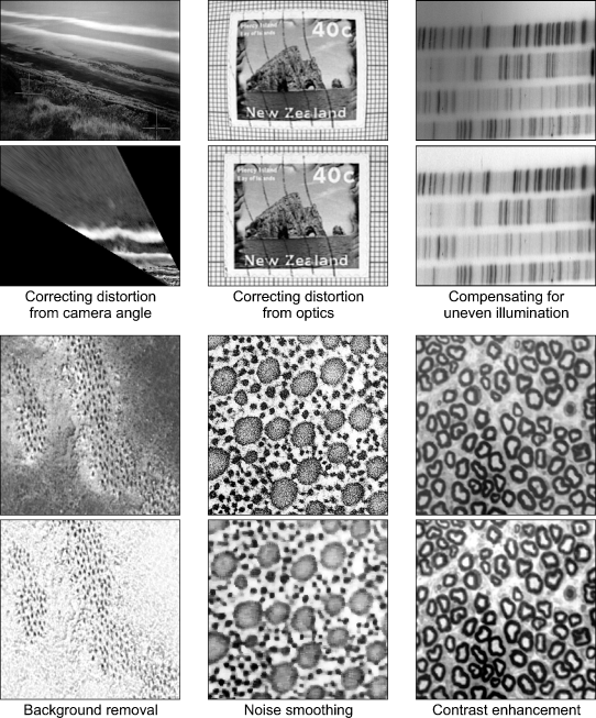
Physical or environmental constraints may mean that the input images are not ideal. To compensate for deficiencies in the image capture process, preprocessing can be used: to remove background or dark current noise; to correct for nonlinearity in the image transfer function; to correct for distortion caused by optics or camera angle; and to compensate for deficiencies in illumination. Image filtering may be used to smooth noise or to enhance and detect edges, lines and other image features. Examples of some of these preprocessing operations are illustrated in Figure 4.2.
Figure 4.2 Example preprocessing operations.
One way of suppressing irrelevant information is to normalise the image content. Intensity normalisation, such as contrast expansion or histogram equalisation can be used to compensate for variations in lighting, reflectivity or contrast. Position and size normalisation may be used to centre, orientate and scale an image or object to match a template or model. This may require an initial segmentation to first locate the object.
Segmentation is the processes of splitting the image into its meaningful components. This can vary from separating objects from the background to separating an image into its constituent parts. Segmentation can be based on intensity, colour, texture or any other local property of the pixel values. There are two broad approaches to segmentation, as shown in Table 4.1. Edge-based methods focus on detecting the boundaries between regions, with the regions defined implicitly by the enclosing boundaries. They usually use edge detection or gradient filters to detect edges and then link the significant edges to form the boundaries. Region-based methods work the other way around. They effectively classify pixels as belonging to one class of objects or another based on some local property, with the edges determined implicitly by changes in property at the region boundary. They are characterised by filtering (to enhance or detect the property used for segmentation; Randen and Husoy, 1999) followed by thresholding or statistical classification methods to assign each pixel to a region. Both edge and region based methods can be performed either globally or incrementally (Bailey, 1991). Global methods perform the segmentation by processing every pixel in the image. Incremental methods only operate locally on the part of the image that is being segmented. They are usually initialised with a seed pixel and work by extending the associated edge or region by adding neighbouring pixels until a termination condition is met. Segmentation may also involve using techniques for separating touching objects such as concavity analysis, watershed segmentation and Hough transform.
Table 4.1 Image segmentation methods.
| Edge-Based Segmentation | Region-Based Segmentation | |
| Global processing | Edge detection and linking | Thresholding |
| Incremental processing | Boundary tracking | Region growing |
The next stage within the algorithm is to extract any required information from the image. In image analysis applications, the measurements are the desired output from the image processing procedure. The measurements may be tangible (physical size, intensity) or abstract (for example, the fractal dimension to quantify roughness (Brown, 1987) or the average response to a particular filter to characterise texture (Randen and Husoy, 1999)). Most tangible measurements require the imaging system to be calibrated to determine the relationship between pixel measurements and real world measurements.
In other applications, a set of image or object feature measurements is used to characterise or classify the image or object. Boundary features are properties of the edges of the object (such as contrast) while region features are properties of the pixels within the region (colour, texture, shading). Shape features consider the whole object (area, height, width, perimeter, enclosing rectangle, number of corners, convex hull area and perimeter, moments, best-fit ellipse, Fourier descriptors etc.). Virtually anything that can be measured, or can be derived from multiple measurements, can be used as a feature. The set of measured features makes up a multidimensional feature vector, with each feature corresponding to a dimension.
Classification is the process of recognising or assigning meaning to an object based on the measured feature vector. Each point in the feature space represents a particular combination of feature values. When an appropriate set of features is chosen, the feature vectors for objects within a class should be similar and fall in the same region of feature space. The classification process therefore involves clustering or segmentation within the feature space. With such a large number of possible features to choose, the feature space potentially has a high dimensionality. However, there is often a strong correlation between many of the features. Choosing the best features to use can be a bit of an art. The goal in selecting the feature set is to choose only as many features as are necessary to distinguish the objects as unambiguously as possible. Obviously, a starting point is to look at the features used to distinguish the objects of interest. An analysis of the covariance can help to identify significant correlations between the features. Where there are strong correlations, consider replacing one or more of the features by a derived feature. For example, the length and width of an object are often correlated, especially as the scale changes. In this case more information can often be obtained from the aspect ratio (length divided by width) than either the length or width. Unless the size or some other feature is used directly to distinguish between classes, it is often better to use dimensionless derived features such as aspect ratio, compactness and so on. Principal components analysis and related techniques can help to identify the features that account for most of the variance in the population.
Given a set of feature vectors (for example those derived from the set of sample images) there is a wide range of techniques used to perform the classification: decision trees, feature template-based classification, Bayesian classification, neural networks, and support vector machines, amongst many others. In most applications, each object within the set of sample images has an associated desired classification. These associations form the training data for the classification. Training is the process of determining the classification parameters that minimise the classification errors. This may be as simple as determining the average feature vector for the objects belonging to each class for feature template classification, or as complex as determining the optimum set of weights for a neural network.
Some applications have no training data but a large number of samples. Unsupervised classification is the process of determining the classes purely from an analysis of the resultant feature vectors. It derives the classification by looking for groups or clusters of samples within the data provided. One example of an unsupervised classifier is K-means clustering (Leeser et al., 2000).
Finally, the data that is extracted may require further processing depending on the application. For example, a Kalman filter may be used for object tracking (Kalman, 1960), or in mobile robotics the data may be used to update a map or to plan a route through the scene. In many computer vision applications, the data derived from the image is used to update the parameters of an underlying model representing the scene.
Once the initial algorithm has been developed, often on only a small set of images, the next step is to refine the algorithm using a wider range of images. The algorithm is tested on the remaining images within the representative sample to ensure that it is able to handle all of the expected conditions in the correct manner. Algorithm refinement is most likely to affect the preprocessing operations to make the complete algorithm more robust. Particular care should be taken to check the algorithm over the full range of lighting conditions that it is expected to operate under.
Very few algorithms are perfect. There are two key points where the algorithm is most likely to fail. The first is segmentation failure, where the object is not correctly segmented from the background. Often a partial segmentation is worse than a complete failure, because the features obtained will generally not reflect those of the complete object. With any segmentation failure, it is important to re-evaluate any assumptions that are made about the task or scene to check that they are not the cause of the failure, and correct these if necessary. If the problem is caused by poor contrast or noise, this may require further preprocessing to correct, or even redesign of the image capture system to obtain better starting images. If possible, the algorithm should detect whether or not the segmentation was successful, or at least act appropriately when it encounters errors. Remember the ‘garbage in, garbage out’ principle – if the image quality is very low, the algorithm is not likely to work reliably.
The second point of failure is classification failure, which can have several causes. The first, and probably most common, is when the feature vector distributions for two or more classes are not completely separated. In the region of overlap in feature space, it is impossible to distinguish to which class an unknown feature vector belongs. One solution is to find an additional feature (or combination of features) that is able to better discriminate between the overlapping classes. Misclassification can also result from under-training, where insufficient samples are used to represent each of the classes adequately. As a result, the region of feature space associated with one or more classes in inaccurately represented. A particular danger occurs if the samples in the training set are not representative and the set of feature vectors obtained is biased in some way. The opposite of under-training is over-training. This can be a particular problem with neural network-based classifiers. An over-trained classifier gives excellent results on the set of images used for training, but gives very poor results on previously unseen images. The classifier is able to recognise the training examples but does not generalise well to other examples of the same class. A fourth cause of classification failure results from using an inappropriate classifier, which does not have the power to make the required distinctions. An example is a neural network with insufficient nodes in the hidden layer, or using linear discriminant analysis when the classes cannot be separated using hyperplanes. Finally, faulty or inaccurate segmentation may result in feature vectors that are outliers of the correct distribution. Such outliers can have an undue influence over the training of some classifiers (for example, support vector machines) and should be eliminated before training.
4.2.3 FPGA Development Issues
The image processing algorithm cannot be developed directly on the FPGA. The main reason is that the development cycle times are far too long to allow interactive design. Assuming that an implementation of the desired operation is available in a hardware description language, the compilation and place and route times required to map it onto an FPGA are prohibitive.
Therefore, the algorithm first needs to be developed in a software environment. For this, any image processing algorithm development environment that satisfies the requirements described in the previous section is suitable. Such an environment will usually be distinct from the FPGA development environment.
One of the advantages of separating the algorithm development from the FPGA implementation is that the application level algorithm can be thoroughly tested before the complex task of mapping the algorithm onto the target hardware. Such testing is often much easier to perform within the software-based image processing environment, which has been designed to facilitate this purpose. Testing the hardware implementation then becomes a matter of verifying that each of the image processing operations has been implemented correctly. If the operations behave correctly, then the whole image processing algorithm will also function in the same way as the software version.
The algorithm development process does not stand alone. The implementation process, as described shortly, is often iterative as the algorithm is modified to make all of the operations architecturally compatible. Whenever any changes are made to the image processing algorithm, it is necessary to retest the algorithm to ensure that it still performs satisfactorily.
Some algorithm testing must be deferred to the final implementation. Evaluating the effectiveness of an image processing algorithm on a continuous, noisy, real-time video stream is difficult in any environment.
The output from the algorithm development step is the sequence of image processing operations required to transform the input image or images into the desired form. It has been tested (within the software-based image processing environment) and shown to meet the relevant accuracy and robustness specifications for the application.
Once an initial algorithm has been developed, it is necessary to define the implementation architecture. It is important to obtain a good match between the architecture and both the application level and operation level algorithms. A poor match makes inefficient use of the available resources on the FPGA and can limit the extent to which the algorithm may be accelerated. Consequently, the system may not meet the targeted speed requirements or the design may require a larger FPGA than is really needed.
The architecture can be considered at two distinct levels. The system level architecture is concerned primarily with the relationship and connections between the components of the system. Three aspects of the system architecture are of primary importance: the relationship between the FPGA and any other processing elements (whether they be a standard computer, or DSP); the nature of any peripherals and how they are connected; and the nature and structure of external memory within the system. The computational architecture is concerned primarily with how the computation of the algorithm is performed. This includes the forms of parallelism that are being exploited and the split between using hardware and software for implementing the algorithm.
On a software-based image processing system, the computational architecture is fixed and the system architecture is generally predefined. For an FPGA based system, however, nothing is provided and all aspects of the architecture must be developed. Once exception to this is perhaps the use of development boards for prototyping, where much of the system level architecture is fixed by the board vendor.
4.3.1 System Level Architecture
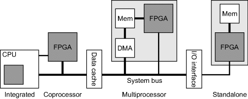
Perhaps the biggest factor of the system architecture is whether the system has a conventional serial computer as a host processor or whether the FPGA stands alone. Compton and Hauck (Compton and Hauck, 2002) identified four distinct ways in which programmable logic could be coupled with a host computer system within this spectrum, as illustrated in Figure 4.3. Todman et al. (2005) added a fifth coupling architecture: that of a CPU embedded within the FPGA (either as an embedded hard-wired core or as a soft core built from the FPGA fabric).
Figure 4.3 Coupling between a host processor and an FPGA. (K. Compton and S. Hauck. “Reconfigurable computing: A survey of systems and software,” ACM Computing Surveys, Vol. 34: 171--210, © 2002 Association for Computing Machinery, Inc. Reprinted by permission.)
In the most closely coupled arrangement, the programmable logic provides reconfigurable functions units integrated within the host CPU. This requires that the programmable logic be built inside the processor and allows instructions to be customised according to the application that is being executed (Hauck et al., 2004). The purpose is to accelerate key instructions within the host processor, while retaining the simplicity of the standard software processing model. Data is usually passed between the reconfigurable logic and CPU through shared registers (Compton and Hauck, 2002).
With modern FPGAs, this approach may be readily taken by building the processor from the logic within the FPGA (the fifth architecture identified by Todman et al., 2005). Such a processor may be augmented with whatever custom instructions the developer requires. However, one limitation of building a custom processor is that the developer also needs to build all of the associated tools (optimising compilers, etc.). This may be overcome by using vendor provided soft-core processors, such as the NIOS II with Altera FPGAs, or MicroBlaze with Xilinx FPGAs. The NIOS allows the provided processor to be augmented with custom instructions. One limitation of custom instructions is the restriction in the amount of data that may be passed to or from the function unit with each instruction, and the limited time that is available to complete the processing. It is usually necessary to stall the main processor if the custom instruction takes a long time to execute.
In the next more loosely coupled configuration, an FPGA can be used as a coprocessor (Miyamori and Olukotun, 1998), to accelerate particular types of operations in much the same way that a floating-point coprocessor accelerates floating-point operations within a standard CPU. In this configuration, the FPGA-based processing unit is usually larger than an ALU or similar functional unit within the host. The coprocessor operates on its data relatively independently of the main processor. The main processor provides the data to be processed (either directly or indirectly) and then triggers the coprocessor to begin executing. The results are then returned after completion (Compton and Hauck, 2002). The operations performed can run for many clock cycles without intervention from the host processor. This allows the host to continue with other tasks, while waiting for the coprocessor to complete. Note that the FPGA-based coprocessor has access to the data from the host's cache.
Using dedicated hardware as a coprocessor is most commonly used when the main application is implemented within software, but time critical or computationally dense sections of an algorithm are accelerated through direct hardware implementation. There may also be multiple hardware processors, each developed to accelerate a critical part of the algorithm.
In the next loosely coupled arrangement, the FPGA system effectively behaves as an additional processor in a multiprocessor system (Compton and Hauck, 2002). This requires the FPGA system to process large sections of an application independently of the host to be the most effective. The FPGA system sits on the system bus, with DMA used to transfer data from the host system memory into local memory. Depending on the processing performed, the results can either be transferred back to the host through DMA, or via registers within the FPGA that are mapped into the address space of the host. The host system configures the FPGA, indicates where the data to be processed is located, and triggers the FPGA system to begin its execution. When processing is complete, this is signalled back to the host processor.
For image processing, the performance is strongly influenced by the I/O bandwidth, the amount of local memory available and its arrangement (Benitez, 2002). The independent processor arrangement also maps well to the image processing pyramid introduced in Figure 1.7, with the lower level operations implemented directly in hardware, and with software used to implement the higher level operations.
In the final configuration, the FPGA operates independently of the host system, which may not even be connected. In this arrangement, the communication with the host is generally sporadic and of relatively low bandwidth. In the stand-alone configuration, usually all of the processing is performed by the FPGA, including any embedded software processor it may contain.
Within image processing, where a large degree of parallelism can be exploited by the operation level algorithms, either multiprocessor or stand-alone configurations are usually the most appropriate. The integrated and coprocessor configurations are usually too tightly coupled to fully exploit parallelism in low level image processing operations.
For high performance computing applications, the hosted multiprocessor configuration is the most common. For image processing, the host is usually responsible for image capture and display, and any user interaction. The host operating system needs to be augmented to enable it to reconfigure the FPGA (Andrews et al., 2004). This is usually dynamic reconfiguration, allowing the host to change the FPGA configuration depending on the application (Wigley and Kearney, 2001; Sedcole et al., 2007). The host operating system is also responsible for distributing tasks between the serial processor and the FPGA system (Steiger et al., 2004; Lubbers and Platzner, 2007), and synchronising communications between all of the processes (both hardware and software) (Mignolet et al., 2003; So, 2007).
The stand-alone configuration performs all or most of the work on the FPGA. This does not necessarily mean that there is no serial processor. Some modern FPGAs have a processor built into them, or it is always possible to include a soft-core processor within the fabric of the FPGA. However, the FPGA is responsible for any image capture and display. Any user interaction must also be built into the FPGA, either as hardware modules, or using the serial processor. Unlike on a conventional serial processor, an FPGA has no operating system (Bailey et al., 2006). If there is an embedded serial processor, this may have an operating system running on it, but the drivers will be limited to common peripherals. Much of the low level interfacing must be built in hardware, and if this is to be interfaced to the processor, device drivers must be written. If no serial processor is used, all of the user interface must be built in hardware (Buhler, 2007).
For debugging and initial development, the stand-alone configuration may have a host computer. This can be used for directly downloading the FPGA configuration and may provide some support for debugging. However, for normal running the FPGA configuration is often loaded directly from flash memory, avoiding the need for a host processor.
Also at the system level is the memory architecture. A key factor to consider is the degree of coupling between the memory, FPGA and any CPU. Only some of the arrangements are shown in Figure 4.3. Distinction also needs to be made between shared system memory and memory local to the FPGA. For local memory, the technology is also an important consideration. Many high speed memories, especially those with large capacity, operate most efficiently in burst mode. In this mode, a predefined number of successive memory locations may be read or written in successive clock cycles. Dynamic memories require separate addressing of the row and column within the memory, sometimes with several clock cycles between the row address and the column address. Dynamic memories also must be refreshed regularly, with access to the memory unavailable during the refresh period.
Other memory technologies may allow random access on successive clock cycles, although for high speed operation they are often pipelined with the address having to be provided one or two clock cycles before the data is available. This may have implications for the speed of some operation level algorithms, especially where the memory address is data dependent.
4.3.2 Computational Architecture
The computational architecture defines how the computational aspects of the algorithm are implemented. A particular focus is the form of parallelism being exploited to achieve the algorithm acceleration. Not all aspects of the algorithm may be amenable to hardware implementation, so a later section focuses more on the split of the application level algorithm between hardware and software execution.
4.3.2.1 Stream Processing
The main bottleneck of software-based image processing is that it is memory bound. An operation reads the pixel values from memory, processes them, and writes the results back to memory. Since each operation performs this, the speed of the algorithm will be largely limited by the number and speed of memory accesses. Stream processing can overcome this bottleneck by pipelining operations. The input data is read once from memory, or streamed from the camera and passed into the first operation. Rather than write the results back to main memory, they are directly passed on to the next operation. This will eliminate at least two memory accesses for each stage of the pipeline: writing the results and reading them again as input for the next operation. The benefits of streaming can therefore be significant.
For embedded vision applications, at some stage the data must initially be read from the camera. If possible, as much processing should be performed on this data while it is passing through the FPGA before it is written to memory. If the whole application can be implemented as a single streamed pipeline then it may not even be necessary to use a frame buffer to hold the image data. Similarly, if an image is being displayed, the pixels need to be streamed to the display. Again, much benefit can be gained by performing as much processing on-the-fly as the data is being streamed out.
One of the key characteristics of stream processing is a fixed clock rate, usually one clock cycle per pixel. This clock rate is constrained by the input (from a video camera) or output (to a display). At the input, each pixel must be processed as it arrives, otherwise the data is lost. Similarly, a pixel must be produced on the output at each clock cycle; otherwise there will be no data to display and the output will appear blank for that pixel. Consequently, the design of stream processing systems is synchronous, at least on the input and output. If every stage of the pipeline can be operated synchronously, then the design is simplified.
Stream processing is well suited to low level image processing operations, such as point operations and local filters, where processing can be performed during a raster scan through the image. If an operation, for example a filter, requires data from more than one pixel, it is necessary to design local buffers for each operation to cache the necessary data. This is because the synchronous nature of stream processing limits memory access to one read or write per clock cycle. To satisfy this constraint, the algorithms for some operations may need to be significantly redesigned from that conventionally used in software. The fixed timing constraint arising from the predetermined constant throughput of stream processing may be overcome by using low level pipelining. This splits a more complex calculation over several clock cycles while maintaining the throughput of one pixel per clock cycle.
4.3.2.2 Systolic Arrays and Wavefront Processing
The idea of stream processing may be extended further to systolic arrays (Kung, 1985). A systolic array is a one or two dimensional array of processors, with data streamed in and passed between adjacent processors at each clock cycle. It is this latter characteristic that gives systolic arrays their name. Since the communication is regular and local, communication overheads are low. A systolic array differs from pipeline processing in that data may flow in any direction, depending on the type of computation being performed. For many systolic arrays, the processing elements in the array are often relatively simple and perform the same operation at each clock cycle. This makes systolic arrays well suited to FPGA implementation.
The difference between a systolic array and a wavefront array is that systolic arrays are globally synchronous, whereas wavefront arrays are asynchronous. A wavefront array therefore requires handshaking with each data transfer. This means that a wavefront array is self-timed and is able to operate as fast as the data is able to be processed. Unfortunately, such asynchronous systems are not well suited to implementation on synchronous FPGAs. However, they may be able to be implemented by self-timed architectures such as the Achronix Speedster (Section 2.4.4).
Systolic arrays work best where the processing is recursive with a regular data structure. The systolic array effectively unrolls the recursive loop to exploit concurrency in a way that uses pipelining to make use of the regular data structure. This makes such an architecture well suited for matrix operations (Kung and Leiserson, 1978) and for implementing many low level image processing operations (Kung and Webb, 1986). They are most suited where the operations are relatively simple and regular, such as filtering (Hwang and Jong, 1990; Diamantaras and Kung, 1997; Torres-Huitzil and Arias-Estrada, 2004), connected component labelling (Nicol, 1995; Ranganathan et al., 1995) and computing the Fourier transform (Nash, 2005). However, a single array is not well matched for implementing a complete application level image processing algorithm. The streamed nature of the inputs and outputs means that a systolic array processor would fit well with stream processing.
4.3.2.3 Random Access Processing
In contrast with stream processing, random access processing allows pixels to be accessed from anywhere in the memory as needed by an operation. Consequently, there are no explicit requirements in the pattern of data access. It requires the image to be available in a frame buffer rather than as an input stream. Random access processing relaxes the hard timing constraint associated with stream processing. If necessary, several clock cycles may be used to process each pixel accessed or output.
Random access processing is, therefore, most similar to software processing. Consequently, it is generally easier to map a software algorithm to random access processing than to stream processing. However, simply porting a software algorithm to hardware using random access processing will generally give disappointing performance. This is because the underlying software algorithm will usually be memory bound and performance will be limited by memory bandwidth. Where possible, steps must be taken to minimise the number of memory accesses by using local buffers. It may also be necessary to design an appropriate memory architecture to increase the memory bandwidth. Some of these mapping techniques are described in the next chapter.
For complex algorithms, the output may not be regular in the sense that there may be a variable number of clock cycles for each pixel produced. This can make it more difficult to synchronise the dataflow between successive operations in the application level algorithm. Therefore, it may be necessary to design synchronisation buffers to manage the uneven data flows. If the inputs and outputs are in a sequential order, then a FIFO buffer provides such synchronisation. Otherwise, synchronisation may require a frame buffer.
The clock speed for random access designs is generally not constrained. Therefore, the throughput can be increased by maximising the clock speed. This may be accomplished by using low level pipelining to reduce the combinatorial delay. The operation level algorithm may be further accelerated by examining the dataflow to identify parallel branches and implementing such operations in parallel.
One form of this data parallelism is to partition different parts of the image to separate processors. This requires multiple copies of the hardware, one for each parallel processor. Each copy will usually have its own local memory to avoid problems with limited bandwidth. However, when considering such parallelism, it is also important to consider not only the operation being parallelised, but also the operations before and after it in the processing chain. One overhead to consider is that required to transfer the data from system memory (such as a frame buffer) to local memory and back. If care is not taken, these overheads can remove much of the performance improvement gained by partitioning the processing. Often the processor will need to be idle during the data transfer phase unless there are sufficient memory resources to enable some form of bank switching to be used.
4.3.2.4 Massively Parallel Architectures
The extreme case of such data parallelism is to use a massively parallel architecture. Such architectures exploit the fact that many image processing operations consist of a series of operations performed independently on each pixel. In software, the outermost loop for such operations will iterate through the pixels within the image. A massively parallel architecture effectively unrolls this outermost loop and implements the iterations on each pixel in parallel. The result is a separate processor for each pixel or block of pixels. A massively parallel processor is able to process whole images in a few clock cycles, regardless of the size of the image. Algorithms that rely primarily on local information can readily be mapped onto such architectures.
While nice in theory, there are two limitations to massively parallel architectures. The first is the communication bottleneck. Massively parallel algorithms work well when the data is already present within the processors. However, getting the data into the array (from the camera) and out of the array (to a display if necessary) can often take longer than the actual processing of the image. A second communication problem occurs if the processing requires sending or receiving data from outside a local region. The communications must either be broken down into a series of local steps, with the processors spending a significant proportion of their time forwarding data, or a hierarchical communication scheme established for longer distance communication and data collection.
The second limitation is that a massively parallel processor requires significant resources on the FPGA, even if each processor is relatively simple. This limits the use of such architectures to small images, or allocating a block of pixels to each processor. For example, both the communication and resource limitations are reduced by allocating one processor to each column or row of pixels within the image.
As a result of these limitations, massively parallel architectures are not considered in detail any further in this book.
4.3.2.5 Hybrid Processing
The best performance can usually be achieved when the whole application can be implemented in a single processing mode and memory access to a frame buffer is minimised. This may require considerable redesign and development of the operation level algorithms to make them architecturally compatible. It may also require modifying the application level algorithm to avoid using operations that do not integrate well with the others.
In some applications, it may not be possible to implement the entire algorithm using stream processing. In such cases, it may be necessary to combine stream and random access processing. The introduction of one or more frame buffers will usually increase the latency of the algorithm. However, for some operations where each output pixel may depend on data from anywhere within the image, this cannot be avoided. With hybrid processing, frame buffer access may be minimised by maximising the use of stream processing.
4.3.2.6 Computational Architecture Design
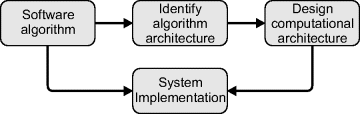
The key to an efficient hardware implementation is not to port an existing serial algorithm, but to transform the algorithm to produce the computational architecture. There are two stages to this process (before implementation), as shown in Figure 4.4.
Figure 4.4 Transforming an algorithm to produce the computational architecture.
The first stage is to analyse the algorithm for the underlying algorithmic architecture. In this process, it is important to look at the whole algorithm, not just the individual operations. This is because gains can be made by considering the interactions between operations, especially if the operations can be made architecturally compatible. A dataflow analysis is one common method of identifying the underlying computational architecture (Johnston et al., 2006b; Sen et al., 2007). This allows the developer to get an overview of the design and investigate how it can be modified. In this process of analysing the algorithm, the underlying algorithm needs to be changed or transformed to one that is more readily able to map efficiently to a hardware implementation.
Several such transformations may be applied to the algorithm (Bailey and Johnston, 2010). The first is to convert as many operations as possible to pipelined stream processing to eliminate intervening frame buffers. Any operation that may be implemented by processing the data in a raster-scanned order through the image can be streamed. Some algorithms that are not naturally streamed may be redesigned to use stream processing (for example chain coding, as described in Section 11.3).
The iterations present in many loops may readily be parallelised. Loop unrolling replaces the innermost loops of an algorithm with multiple sequential copies of the operations within the loop construct. This allows longer pipelines to be constructed at the expense of additional hardware. With many image processing operations, these innermost loops are inherently parallel (for example weighting the pixels within a linear filter) and it is only the sequential nature of a serial processor that requires a loop. Strip mining is related to loop unrolling in that it creates multiple parallel copies of the loop body. The difference is that each copy operates on a different section of the data. The computation is accelerated by partitioning the input data over different hardware processors.
A less common transformation is strip rolling and multiplexing. Sometimes, after strip mining, only one of the parallel processing units is active in any clock cycle. For example, using stream processing to find the bounding boxes of objects requires operating on multiple objects in parallel. However, a pixel can only belong to one object, so in any clock cycle, only one bounding box processor will be operating. In this case, strip rolling replaces the multiple processing units with a single processor that is multiplexed between the different instances.
In some algorithms, it is possible to rearrange the order of the operations to simplify the processing complexity, or even eliminate some steps. A classic example of this is greyscale morphological filtering followed by thresholding. This sequence of operations is equivalent to thresholding first, followed by binary morphological filtering. The algorithms for binary filtering are significantly simpler than those for greyscale filtering, resulting in considerable hardware savings and often a reduction in latency.
The data can sometimes be coded to reduce the volume, and hence the processing speed. Run length coding is a good example. After the data has been run length coded, whole runs of pixels can be processed as a group, rather than as individual pixels. For example, Appiah et al. (2008) used run length coding to accelerate the second pass through the image for connected components labelling.
Gains can often be made by substituting one or more image processing operations with other, functionally similar, operations. Substitutions may involve approximating operations with similar but computationally less expensive operations. Common examples are replacing the L2 norm in the Sobel filter with the computationally simpler L1 or L∞ norm (Abdou and Pratt, 1979), or modifying the coefficients used for colour space conversion to be powers of two (Sen Gupta et al., 2004). Note that substituting an operation may change the results of the algorithm. The resulting algorithm will be functionally similar but not necessarily equivalent. In many applications, this does not matter, and the substitution may enable other transformations to be applied to improve the computational efficiency.
The second stage is to design the computational architecture that is implied by the algorithm architecture. This may require further transformation of the algorithm to result in a resource efficient architecture that can effectively exploit the parallelism available through a hardware implementation. Some of the techniques that may be used for this will be described in more detail in the next chapter. Operation specific caching of data ensures that data which is used multiple times will be available when needed. Low level pipelining and retiming can be used to reduce the combinatorial delay and increase the clock speed. It is also necessary to select appropriate hardware structures that correspond with data structures used in the software algorithm.
The design process can be iterative with the algorithm and architecture mappings being updated as different design decisions are made. However, with a thorough design at this stage, the final step of mapping the algorithm onto the architecture to obtain the resultant implementation is straightforward.
4.3.3 Partitioning between Hardware and Software
Low level image processing operations that can readily exploit parallelism are ideal for hardware implementation. Such operations are relatively slow when implemented in software simply because of the volume of data that needs to be processed.
However, not all algorithms map well to a hardware implementation. Tasks that have dynamically variable length loops can be clumsy to implement in hardware. Those with complex control sequences (Compton and Hauck, 2002) are more efficiently implemented in software. Such tasks are characterised by large amounts of complex code that is primarily sequential in nature. If implemented in directly in hardware, this would require significant resources because each operation in the sequence would need to be implemented with a separate hardware block. If there is little scope for exploiting parallelism, much of the hardware will be sitting idle much of the time. The same applies for functions that are only called occasionally, for example once or twice per frame (or less). These tasks or operations can be implemented more easily and more efficiently in software.
Two broad classes of tasks or operations that are best implemented in software are high level image processing operations (for example object tracking; Arias-Estrada and Rodríguez-Palacios, 2002) and managing complex communications protocols. High level image processing operations are characterised by a lower volume of data and more complex control patterns. Many provide limited opportunities for exploiting parallelism and often the computation path is dependent on the data being processed. Similarly, communications such as TCP/IP require a complex protocol stack that can be unwieldy to implement in hardware. While it is possible to implement these tasks in hardware (see, for example Dollas et al., 2005, for a TCP/IP implementation), it can be more efficient in terms of resource utilisation to implement them in software. Software also has the advantage that it is generally easier to programme.
The approach taken to partitioning the application between hardware and software will depend significantly on the system level architecture and, in particular, the level of coupling between the software processor and programmable logic. The software processor may consist of a separate CPU or be integrated on the FPGA as a hardware core (such as the PowerPC core within the Xilinx Virtex Pro) or as a soft core implemented using the FPGAs programmable logic. There is also a wide range of standard processor cores available that have FPGA implementations, including common microcontrollers (8051, 68HC11, PIC) and digital signal processors (320C25). One advantage of using a standard processor is that all of the application development tools for that processor can be used. In particular, using the integrated high level language development and emulation tools for the processor can speed code development and debugging of the software components.
Therefore, the choice is not just whether to implement the application in either software or hardware. There is a spectrum of partitioning of the application between the two, ranging between full software and full hardware implementations as illustrated in Figure 4.5.
Figure 4.5 Spectrum of hardware and software mix. Note that the CPU can be either external or integrated within the FPGA.
At the instruction level of granularity, the application can be largely implemented in software, with the FPGA used to implement custom instructions. This allows the programme to ‘call’ hardware acceleration blocks (Arnold and Corporaal, 2001). For image processing, it is impractical to implement the whole algorithm this way. However, this approach can be used to augment the processor for the software component of the application where groups of instructions are clumsy or inefficient when implemented purely in software.
The partitioning can also be at the task level of granularity, where whole tasks are assigned either to a software or hardware processor. The hardware and software tasks operate relatively independently of each other, only communicating when necessary. This would allow, for example, the image capture and low level image processing operations to be implemented in hardware, with the results being passed to high level image processing operations implemented in software.
If the software tasks are of low complexity, then an alternative to using a full CPU is to design a simplified serial processor. This can be either a lightweight soft core (such as the picoBlaze) or a completely custom processor. One limitation to using a custom processor is that compilers and other development tools will not be available and the software for the processor must generally be written in assembly language. At the extreme end, the sequential components of the algorithm could be implemented using a finite state machine. Quite sophisticated, memory-based, finite state machines can be implemented with a small resource footprint (Sklyarov, 2002; Sklyarov and Skliarova, 2008), effectively making them custom processors.
Regardless of the level of partitioning, it is essential to clearly define the interface and communication mechanisms between the hardware and software components. In particular, it is necessary to design the synchronisation and data exchange mechanisms to facilitate the smooth flow of data. In the final design, it is also important to take into account the communication overhead between the hardware and software portions of the design.
One advantage of using a standard processor is the availability of standard operating systems such as Linux. Using an operating system such as embedded Linux has an advantage that all of the features of the standard operating system are available, subject to the limitations of the memory available within the system (Williams, 2009). It also provides a familiar development environment for the software components, including the ability to develop and test the software on one platform before transferring it to the FPGA. One feature of particular interest is that Linux has a full TCP/IP stack enabling the complete system to be networked relatively easily. This can significantly extend the functionality of the system, even if the software processor is not used directly for the application. Having a TCP/IP interface enables:
- an efficient means of communicating images and other data between devices in a distributed system;
- a Web interface for control and setting of algorithm parameters, and for viewing the results of processing;
- remote debugging through telnet, and even mounting the file system across the network;
- the ability to remotely update the configuration.
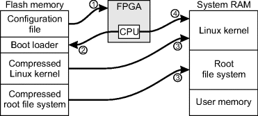
A minor disadvantage of using an embedded Linux is that even a minimal system will require off-chip RAM. A minimal Linux kernel will require approximately 4 MB of additional flash memory and 16 MB of DDR system memory. The system memory should be solely for the use of the embedded processor and be separate from any memory directly accessed from the user logic on the FPGA. As the number of support applications (within Linux) is increased, the memory requirements (both flash and RAM) will increase accordingly. The boot process of the system is as follows (Figure 4.6) (Gregori, 2009):
1. The FPGA configuration is loaded from flash memory. This configures the FPGA, including the processor on the FPGA.
2. When the system starts running, the processor executes the boot loader from the flash memory.
3. The boot loader decompresses both the Linux kernel and the root file system from flash, and copies them into RAM.
4. Using the RAM image, the processor starts execution of the Linux kernel and associated services.
When interfacing between the hardware and software running under embedded Linux, it is best to make the interface through a Linux device driver (Williams, 2009). While it is possible to interface directly from the software to the hardware, using a device driver will make access to the hardware more portable, and make the interface easier to maintain and manage. The Linux kernel effectively provides an API and will provide locking and serialisation on the device.
Figure 4.6 Embedded Linux boot process.
One limitation of using a multitasking operating system is the variable latency of the software components, especially if virtual memory is used. Care must be taken when using such systems in a hard real-time context, especially where software latency is critical. In other cases an embedded Linux can simplify the development and debugging, especially of stand-alone systems.
The key requirement of architecture selection is choosing the most appropriate architecture for the algorithm, both at the computational and system levels. In an embedded application, most of the performance gains come through exploiting parallelism. Power considerations often require maintaining a low clock speed. Careful design of the image processing algorithm can often allow the low level vision to operate at the input or output video rate, which is often up to two orders of magnitude slower than current high end serial processors.
Image capture and display almost always operate on streamed data. Therefore, as much processing as possible should be performed on-the-fly either as the image is streamed in, or streamed out. This will minimise the number of memory accesses required and the sequential nature of the accesses will simplify memory system design.
The final stage within the design process is system implementation. This is where the image processing algorithm is mapped onto the chosen hardware resources as defined by the architecture. The steps here differ significantly from software-based design, where implementation primarily consists of coding the algorithm. An FPGA-based implementation requires designing the specific hardware that will perform the required image processing operations.
Not all of the operations in the algorithm will necessarily map well to hardware. To gain maximum benefit of the parallelism offered by the FPGA, all of the individual operations must be architecturally compatible. If the image processing algorithm has not been developed with the computational architecture in mind, then it may be necessary to modify the algorithm so that the operations better match the selected architecture. This may require the selection of alternative operations where necessary.
The application level algorithm is created at a relatively high level of abstraction, in terms of individual image processing operations. Some of these operations can be quite complex, and all have their own operation level algorithms at a lower level of abstraction. Many of these operations can be implemented using several possible algorithms. The operations within the software-based image processing environment will have been optimised for serial implementation within that environment. Simply porting that algorithm onto the FPGA will generally give relatively poor performance, because it will still be predominantly a serial algorithm. Sometimes the serial algorithm may have a relatively simple transformation to make it suitable for parallel hardware. More often, however, the underlying algorithm may need to be completely redesigned to make it more suitable for FPGA implementation, as described in the previous section. In this case, it may be better to first re-implement the operation using the new algorithm within the image processing environment, where it can be tested more easily, rather than attempt to directly develop and test it on the FPGA.
Since each image processing operation is considerably simpler than the complete application, this can make the implementation easier to test and debug. Standard test bench techniques can be used to exercise the operation through simulation within the FPGA development environment. For individual operations, most of these tests require a much smaller range of possible inputs than the complete application, so most operations can be tested with relatively small data sets rather than with complete images. The FPGA development platform is also implemented on a standard serial computer, so the simulation of a parallel architecture on a serial computer is usually quite time consuming. This is especially the case for clock-accurate simulations of complex circuits with large data sets (images). Therefore, it is better to test as much of each operation as possible using much smaller data sets.
If the algorithm for an operation is complex, or the mapping from software to hardware is not straightforward, incremental implementation techniques are recommended. For this, each stage or block of the algorithm is simulated as it is completed, rather than leaving testing of the complete operation to the end. This approach generally enables errors in the implementation to be found earlier and corrected more easily.
Another task that is required for FPGA-based designs is to develop the interface logic required by peripherals attached to the FPGA. Intellectual property cores may be available for some devices, such as common memory chips, USB ports and so on. For others, these will need to be developed as part of the implementation process. Example interfaces for some specific devices are developed in Chapter 12. These interface blocks may be thought of as device drivers within a conventional operating system. Even if the design uses an embedded CPU running a conventional operating system such as Linux, it will still be necessary to develop the hardware interface between the processor and the external device.
Despite efforts to make programming FPGAs more accessible and more like software engineering (Alston and Madahar, 2002), efficient FPGA programming is still very difficult. It is important to realise that programming FPGAs is hardware design, not software design. Although the languages may look like software, the compilers use the language statements to create the corresponding hardware. Rather than executing the statements on a common, shared, ALU, each statement builds independent, parallel, hardware. Concurrency and parallelism are implicit in the hardware that is built and the compilers have to build additional control circuitry to make them execute sequential algorithms (Page and Luk, 1991). Consequently, sequential algorithms ported from software will by default run sequentially, usually at a significantly lower clock speed than high end CPUs. Some compilers can automatically make minor changes to the algorithm to exploit some of the parallelism available, and this is often sufficient to compensate for the lower clock speed. However, the algorithm is still largely sequential unless it has been specifically adapted for parallel execution. The software-like languages are in reality hardware description languages, and efficient design requires a hardware mindset.
4.4.1 Mapping to FPGA Resources
While it is not necessary to perform the design at the transistor or gate level, it is important to be aware of how the resources of the FPGA are used to implement the design, whether explicitly or implicitly.
Both arithmetic and logic functions are implemented as combinatorial hardware using the configurable logic blocks on the FPGA. Depending on the size of the lookup tables, each logic cell can implement any arbitrary logic function of between three and seven binary inputs, with or without a register on the output. Functions with more inputs are implemented by cascading two or more logic cells.
A simple logic function, such as AND or OR between two N-bit operands may be implemented using N LUTs, one for each bit of the operands. For more complex logic operations, the number of LUTs required will depend primarily on the number of inputs rather than the actual complexity of the logic. In many situations, logical inversion may be obtained for free, simply by modifying the contents of the corresponding LUTs.
Addition and subtraction also map onto combinatorial logic. The carry propagation may be implemented using circuits for ripple carry, or more advanced look-ahead carry or carry select designs (Hauck et al., 2000). Most FPGAs implement dedicated carry chain logic that can be used to speed up carry propagation by reducing routing delays and avoiding the need for additional hardware to implement the carry logic. Counters are simply adders (usually adding a constant) combined with a register to hold the current count value.
Relational operators compare the relative values of two numbers. The simplest is testing for equality or inequality, which requires a bit-wise comparison using exclusive NOR, and combining all of the outputs with a single gate to test that all bits in the two numbers are equal. A comparison operation may be implemented efficiently using a subtraction and testing the sign bit. This has longer latency than testing for equality because of the carry propagation. Therefore, if the algorithm involves any loops, tests should be made for equality rather than comparison, if possible, to give the smallest and fastest circuit.
Multiplication can be performed using a combination of shift and addition. If time is not important, this can be implemented serially using not much more logic than an adder. Unrolling the loop results in an array of adders that combines the partial products in parallel. Although, in principle, the length of the carry propagation may be reduced using a Wallace (Wallace, 1964) or Dadda (Dadda, 1965) adder tree, in practise this gives a larger and slower implementation than using the dedicated carry logic of the FPGA (Rajagopalan and Sutton, 2001). Additional logic is required to perform the carry save additions, and the structure is not as regular as a simple series of adders resulting in increased routing delays. If necessary, the parallel multipliers can be pipelined to increase the throughput. Most current devices (especially those targeted at DSP applications) have dedicated hardware multiplication circuits. These provide faster and smaller multipliers because they do not suffer from FPGA routing delays between stages. However, the multipliers are available only in fixed bit widths. A single multiplier may readily be used for smaller sized words, but for larger word widths either several multipliers must be combined or a narrower multiplier supplemented with programmable fabric logic to make up the width.
In principle, division is only slightly more complex than multiplication, with a combination of shift and subtraction to generate each bit of the quotient. With the standard long division algorithm (for unsigned divisor and dividend), if the result of the test subtraction is positive the quotient bit is 1 and the result of the test subtraction retained. However, if the test subtraction result is negative then the corresponding quotient bit is 0 and the test subtraction discarded, restoring the partial remainder to a positive value. This requires that the carry from each subtraction must completely propagate through the partial remainder before the sign bit can be determined. The algorithm speed may be improved (Bailey, 2006) by using non-restoring division, which allows the partial remainder to go negative. With this scheme, the divisor is added rather than subtracted for negative partial remainders. The major limitation to the speed of division is the propagation delay of the carry rippling through the whole partial remainder at each iteration. An obvious solution is to reduce the number of iterations by determining more quotient bits per iteration (using a higher radix). Another approach is to reduce the propagation delay by reducing the length of the critical path. The SRT algorithm (named after Sweeney, Robertson (1958) and Tocher (1958)) achieves this by introducing redundancy in the quotient digit set. This gives an overlap in selecting between adjacent digits, which allows a quotient digit to be determined from an approximation of the partial remainder (hence does not need to wait for the carry to propagate fully). Two disadvantages of the SRT method are that the divisor must be normalised (so that the MSB is 1) and the quotient digits must be converted to standard binary, both of which require additional logic and time. All of these algorithms may be implemented sequentially to reduce hardware requirements at the expense of throughput, or can be pipelined to increase the throughput. There are also many other advanced algorithms (Tatas et al., 2002; Trummer, 2005). An alternative approach if high speed multipliers are available is to take the reciprocal of the divisor (using lookup tables or fast iterative methods) and then multiply.
In all of the operations described so far, if one of the operators is always a constant, the hardware can be simplified. This can often result in a reduction in both the logic required and the propagation delay of the circuits.
Another logic circuit that is commonly a part of FPGA designs is the multiplexer. These are required when writing to a register or memory from multiple hardware blocks to select the data source being written. A multiplexer is also required on the address lines of memory to select the address source when accessing memory from multiple points in the hardware. Typically, two input bits are required for each bit of the source word (Figure 4.7); one bit for the data value, and one bit to select or gate that source to the output. When many sources are used, the multiplexers may require a significant fraction of the FPGA resources available. There are two types of multiplexer commonly used, corresponding to the use of positive and negative logic (the differences are shown in Figure 4.7). With positive logic, the default output is 0 and a logic 1 is used to gate (or select) the inputs
(4.1) ![]()
Figure 4.7 Multiplexer circuits for data selection. Left: using positive logic; right: using negative logic.
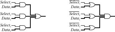
With negative logic, the levels of the input and output are inverted making the default output a 1. De Morgan's theorem is used to convert the expression into a product of sums form:
(4.2) ![]()
This would normally have little effect on the operation of the circuit (provided the correct polarity select signals are generated) except when multiple sources are enabled simultaneously. In this error condition, the logic levels from the two sources are combined; for positive logic the output is the OR of the enabled inputs, whereas for negative logic it is the AND of the inputs.
Modern FPGAs also provide memory resources at a range of granularities. At the lowest level, registers may be built up of from the flip-flops associated with the logic blocks. In most devices, each logic cell has one flip-flop available on its output, so an N-bit register would require N logic cells. The outputs of these flip-flops are always available for use by other logic, so all of the registers in an array would be available at every clock cycle. An array constructed of registers, if accessed using a variable index, would require one or more multiplexers on the output to select the data from the required register. Similarly, writing to an array may also require a multiplexer on the input of each register in the array.
The LUTs within the logic cells of some FPGAs can also be configured as fabric memory, providing 16, 32, or 64 memory locations depending on the available size of the LUTs. These are true memories, with the address decoding and data multiplexing performed using dedicated logic within the logic cell. Note that only one bit is accessible for either reading or writing per clock cycle. Some FPGAs allow the inputs to an adjacent logic cell to be configured as a second port, enabling two accesses per clock cycle. Multiple logic cells can be combined in parallel to create arbitrary width memories. In doing so, each parallel memory will share the same address inputs. Fabric RAM is best suited for small, shallow memories because any increase in the depth requires the use of external decoding and multiplexing. Examples where fabric RAM would be used include storing coefficients or parameters that do not have to be accessed simultaneously, and short FIFO buffers.
Modern FPGAs also have available larger blocks of RAM. These generally have flexible word widths from 1 to over 64 bits wide. Most such RAM blocks are dual-port. The size makes them well suited for row buffers for image processing, for larger size FIFO buffers or for distributed data caching. The RAM can also be used as instruction and data memory for internal CPUs (both hard and soft core).
Some of the larger FPGAs have sufficient memory blocks to hold whole images on chip. However, image frame buffers are more likely to be held off-chip. The number of parallel external RAMs (and ROMs) and their size are limited only by the I/O resources available. Off-chip RAM can also be used for other large blocks of intermediate data storage or be used by an internal CPU to hold data and instructions for larger programmes.
A software processor, if used, can be implemented either on the FPGA or as a separate chip. Large modern FPGAs have sufficient resources on chip not to need an external processor. However, when using an operating system such as an embedded Linux, an external memory is essential.
4.4.2 Algorithm Mapping Issues
As mentioned earlier in this chapter, mapping is not simply a matter of porting the set of operation level algorithms onto the FPGA, unless they were developed with hardware in mind. The key thing is to map what the software is doing by adapting the algorithm to the hardware.
Again, it is important to keep in mind the different levels of abstraction. At the higher level, the application level algorithm should be thoroughly tested on a software-based platform before mapping the operations to hardware. In some situations, it may be necessary to substitute different image processing operations to maintain a uniform computational architecture if possible. Generally, though, the application level algorithm should not change much through the mapping process.
Mapping the individual image processing operations is a different story. The operation level algorithm may change significantly to exploit parallelism. For some operations, the transformation from a serial to parallel algorithm is reasonably straightforward, while for others a completely new approach, and algorithm, may need to be developed.
During the mapping process, it can be worthwhile to consider not just the operations on their own, but also as a sequence. It may be possible to simplify the processing by combining adjacent operations and developing an algorithm for the composite operation. An example of this is illustrated in Section 11.4 with connected components analysis. In other instances, it may be possible to simplify the processing by splitting a single operation into a sequence of simpler operations. An example of this is splitting a separable filter into two simpler filters. In some situations, swapping the order of operations can reduce the hardware requirements. For example, following a greyscale morphological filter with thresholding requires a more complex filter than its equivalent of first performing the thresholding and then using a binary morphological filter.
One of the major issues facing the algorithm mapping process for embedded, real-time image processing is meeting the various constraints. There are three main constraints facing the system designer: timing constraints, memory bandwidth constraints and resource constraints.
Any real-time application will have timing constraints. These are of two types: throughput and latency. Stream processing has a throughput constraint, usually of processing one pixel every clock cycle. If this rate is not maintained, then data streamed from the camera may be lost, or data streamed to the display may be missing. Since the processing performed per pixel will usually take significantly longer than one clock cycle, it is necessary to use pipelining to maintain the throughput. The other timing constraint is latency. This is the maximum permissible time from when the image is captured until the results are output or an action is performed. Latency is particularly important for real-time control applications where image processing is used to provide feedback used to control the state. Delays in the feedback of a control system (caused in this case by the latency of the processing) will limit the response time of the closed loop system and can make control more difficult. In particular, excessive delay can compromise the stability of the system.
Closely related to the timing constraint is the memory bandwidth constraint. Each memory port may only be accessed once per clock cycle. On-chip memory is usually less of a problem because such memory consists of a number of relatively small blocks, each of which can be accessed independently. Off-chip memory, on the other hand, tends to be in larger monolithic blocks. Operations where the computation order does not correspond to the raster order usually require the whole frame to be buffered. The large size of the image buffer generally restricts the frame buffer to be in off-chip memory. Consequently, it can be difficult to read more than one pixel per clock cycle. This can be further complicated by pipelined memory architectures, where the address needs to be provided several clock cycles before the data is available. Operations where the next memory location depends on the results of processing at the current location (for example chain coding) exacerbate this problem. For the memory bandwidth not to seriously limit the processing speed, it is often necessary to transfer data from off-chip memory into multiple blocks of on-chip memory where the bandwidth constraints are more relaxed.
The third area of constraint relates to the resources available on the FPGA. The cost of an FPGA generally increases with increasing size (in terms of the number of logic blocks, memory etc.). When targeting a commercial application, to minimise the product cost it is desirable to use an FPGA that is only as large as necessary. However, even the largest FPGA has finite resources. It is therefore important to make efficient use of the available resources. Using fewer resources can also improve the timing in two ways. The first, and more obvious, is that an algorithm that uses fewer resources will generally have a shorter delay simply because of the shallower logic depth. The second is that a more regular design will be easier to route on the FPGA, and will have a shorter routing delay. As the design approaches the capacity of the FPGA, it becomes increasingly harder to route efficiently and the maximum clock speed of the design decreases.
A second issue relating to resources is contention between shared resources. A parallel implementation will have multiple parallel blocks working concurrently. In particular, only one process can access memory or write to a register in any clock cycle. Concurrent access to shared resources must either be scheduled to avoid conflicts, or additional arbitration circuitry must be designed to restrict access to a single process. Arbitration has the side effect of delaying some processes, making it more difficult to determine the exact timing of tasks.
Techniques for addressing timing, bandwidth and resource constraints are discussed in more detail in the next chapter.
4.4.3 Design Flow
A more detailed sequence of steps for the design process that we follow in our research group is shown in Figure 4.8. The image processing algorithm is developed either using VIPS (Bailey and Hodgson, 1988) or MATLAB® (Gonzalez and Woods, 2004; Solomon and Breckon, 2011). Both are rich algorithm development environments. VIPS was designed specifically for image processing; MATLAB® is more general, but with the image processing toolbox is also targeted for imaging applications. Both are extensible, operations for VIPS are written in C++, whereas for MATLAB® extensions may be written in C or as MATLAB® scripts (m-files).
Figure 4.8 Design flow for FPGA-based implementation of image processing algorithms.
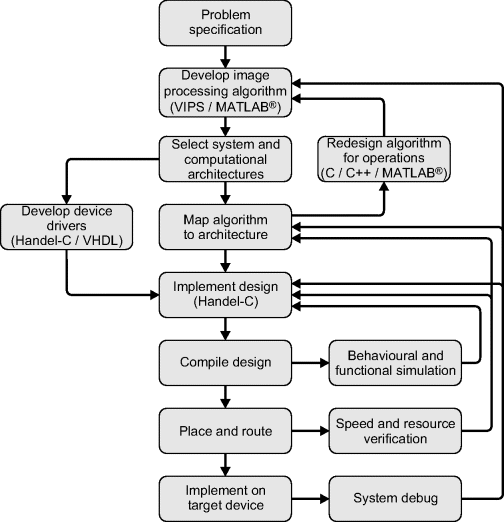
At Massey University Handel-C has been used for the hardware description language because it describes hardware at a higher level of abstraction than Verilog or VHDL. It also allows hardware to be described at a low level where necessary. Where possible, Handel-C is also used for any device drivers. VHDL is only used at the very lowest levels, where Handel-C does not provide sufficient control over the detailed implementation.
Incremental development techniques are used. As each operation is mapped to Handel-C, the simulator within the development environment is used to verify that the operation functions correctly. If each operation performs as designed, then the complete application level algorithm will function as developed and tested within the image processing environment.
FPGA vendor tools are used to place and route the design onto the FPGA resources. The output from this process will indicate whether there are sufficient resources available on the target FPGA. It also provides timing information based on the actual resources used. Feedback from this process is used to modify the algorithms or implementation where necessary to meet timing constraints.
The final step is to download the configuration file onto the target device for system testing. As part of the debugging process, sections may require re-implementation, remapping or, in the worst case, redevelopment.
4.5 Designing for Tuning and Debugging
4.5.1 Algorithm Tuning
Many application level algorithms require tuning to function correctly. Most algorithms have threshold levels or other parameters that must be optimised to obtain the best performance.
If these parameters are hard wired into the implementation, then whenever a parameter is changed, the whole algorithm needs to be recompiled and remapped to hardware – a process that is very time consuming. Therefore, it is best to store these parameters in registers, where they may be readily modified. While it is technically possible to modify the register values directly in the bitstream before downloading onto the FPGA, for example using JBits (Guccione et al., 1999) or RapidSmith (Lavin et al., 2010) with Xilinx FPGAs, Xilinx is currently the only manufacturer to provide the tools for doing this (Graham et al., 2001). In some ways, tuning an algorithm is a little like tuning a car. Recompiling the application is a little like rebuilding the complete engine each time an adjustment is required. Modifying the bitstream is like turning the engine off, making the adjustments, and then restarting the engine with each modification. Instead, it is much more convenient to tune the engine while it is running. Similarly, the best time to modify many of an algorithm's parameter values is while the algorithm is running.
Changing parameters dynamically requires building the hardware to update the parameters. It also requires some form of user interface that enables the developer to adjust or provide new values. When running in a hosted configuration, the host system can provide the user interface and write the control parameters to registers on the FPGA. However, with a stand-alone configuration, the user interface must also be built on the FPGA. This can be either in hardware or on an embedded processor. At the minimum, it must provide a mechanism for selecting and modifying the parameters. With many applications, though, it is usually necessary to provide additional information on the context of the parameters being adjusted. This often involves displaying the image or other data structures at intermediate stages within the algorithm, as illustrated in Figure 4.9 for a simple colour tracking application.
Figure 4.9 Algorithm tuning may require considerable additional hardware to provide appropriate feedback or interaction with the user.
In this application, the complete algorithm can be implemented using stream processing, without the need of a frame buffer. However, to set the threshold levels used to detect the coloured targets, it may be necessary to display histograms of red, green and blue components of the image, or of the ![]() components used for colour thresholding. Since the primary thresholding will be performed in the
components used for colour thresholding. Since the primary thresholding will be performed in the ![]() plane, it is also useful to accumulate and display a two-dimensional
plane, it is also useful to accumulate and display a two-dimensional ![]() histogram of the image. One way of setting the threshold levels is to click on the coloured objects of interest in the input image and use these to initialise or adjust the threshold levels. It is also useful to see the output image after thresholding to see the effects of adjusting the levels, particularly on the boundaries of coloured regions. Similarly, it is also useful to see the effects of the morphological filter in cleaning up the misclassification noise. Finally, it may be useful to include a box generator to overlay the bounding boxes of the detected regions over the top of the original image (or indeed after any of the other processing stages).
histogram of the image. One way of setting the threshold levels is to click on the coloured objects of interest in the input image and use these to initialise or adjust the threshold levels. It is also useful to see the output image after thresholding to see the effects of adjusting the levels, particularly on the boundaries of coloured regions. Similarly, it is also useful to see the effects of the morphological filter in cleaning up the misclassification noise. Finally, it may be useful to include a box generator to overlay the bounding boxes of the detected regions over the top of the original image (or indeed after any of the other processing stages).
Although this example probably provides more contextual information than is really needed, it does illustrate that the additional logic and resources required to support tuning may actually be more extensive than those of the original application. One way to manage these extra requirements is to use two separate FPGA configurations – one for tuning and the other for running the application. The tuning configuration does not need all of the application logic, for example the final control block in Figure 4.9 may be omitted. The tuning configuration can then store the tuning parameters in flash memory (or other non-volatile memory) where they can be retrieved by the actual application configuration.
4.5.2 System Debugging
In many ways, the requirements for debugging the algorithm and system are similar to tuning. In particular, it may be important to see the results of processing after each of the operations to verify that each operation is functioning correctly. This may require the stand-alone configuration to support video output even if the application does not explicitly require it.
System failure can be the result of two main causes. The first is algorithm failure and the second is a result of not meeting timing constraints.
Since it is much harder to debug a failing algorithm in hardware than it is in software, it is important to ensure that the algorithm is working correctly in software before mapping it onto the FPGA. It is essential that any modifications made to the operation level algorithms during the mapping process be tested in software to ensure that the changes do not affect the correct functioning. However, while it is possible to test the individual operations to check that they function correctly, it is not possible to exhaustively test the complete application level algorithm. In many real-time video processing applications, every image that is processed is different. Failures, therefore, should not be a result of the algorithm not working at all, but be intermittent failures resulting from the algorithm not being completely robust.
Unfortunately, the intermittent nature of such algorithm failures makes them hard to detect. Many, if not most, of the images should be processed correctly. Therefore, to investigate the failures, it is necessary to capture the images that cause the algorithm to fail. One way of accomplishing this is to store each of the images before it is processed. Then when a failure occurs during testing, the input image that caused the failure will be available for testing. Such testing is actually easier to perform in software, either in the image processing development environment or through simulation of the hardware in the FPGA development environment.
Algorithm debugging in hardware is much more complex. Additional user controls may be required to freeze the input image to enable closer examination of what is happening for a particular input. It may be important to view the image after any of the operations, not just the output. This may require stepping through the algorithm one operation at a time, not only in the forward direction, but also stepping backwards through the algorithm to locate the operation that is causing the algorithm to fail. The additional hardware to support these controls is shown in Figure 4.10.
Figure 4.10 Instrumenting an image processing algorithm for debugging. The frame buffer enables the input image to be frozen and fed through the algorithm. The results of any of the steps may be routed to the display (stream processing is assumed here).
Note that if stream processing is used, it is not necessary to have a frame buffer on the output; the output is generated on-the-fly and routed to the display driver. However, non-streamed operations or non-image based information may require a frame buffer to display the results.
At a lower level, debugging the internals of an operation is more difficult. Again, it is emphasised that such debugging should be performed in software or through simulation if possible. The advantage of software debugging is that in software each clock cycle does relatively little compared with hardware where a large number of operations are performed in parallel, and the system state can change considerably (Graham, 2001).
Simulation is only as reliable as the simulation model used. The models can be validated by directly comparing the results of simulation with hardware execution over the full range of situations that may be encountered (Graham, 2001). This is particularly useful for identifying problems (both functional and timing) associated with device drivers or other interfaces.
If the design must be debugged in hardware, there are a number of ways in which this may be performed (Graham et al., 2001). Perhaps the simplest approach is to route key signals to unused I/O ports to make them observable from outside the FPGA. An external oscilloscope or logic analyser is then required to monitor the signals. This concept may be extended further by embedding a logic analyser within the design. Both Xilinx (ChipScope; Xilinx, 2008a) and Altera (SignalTap; Altera, 2008e) provide cores that use memory within the FPGA to record internal signals, and later read these recorded signals out to an external companion software package. It is also possible to build dedicated hardware to perform a similar function, recording signals of interest within a block RAM and using the configuration readback mechanism to obtain the data. One limitation of modifying the circuit to include signal probes and additional signal recording hardware is that that these can affect how the connections are routed on the FPGA. These affect the timing and can even change the critical paths, possibly masking or creating subtle timing problems that may occur when the modifications are either present or absent (Graham, 2001; Tombs et al., 2004).
Configuration readback can be used to sample the complete state of a design at one instant. The difficulty with this approach is to associate the logical design with the hardware state of the mapped resources on the FPGA. Signal names, or even the circuit, can be altered for optimisation or other reasons, and with fabric RAM the address pins may be reordered to improve design routability (Graham, 2001). In spite of these limitations, configuration readback provides the widest observability of the design (Graham, 2001). It is possible to add only a little logic to stop and restart execution by gating the clock (Tombs et al., 2004). These features enable hardware single stepping and, with a little extra logic to detect key events, can effectively provide hardware breakpoints. A key limitation of readback-based methods is that they require the clock to be stopped. This makes them impractical for timing verification and, in particular, for testing of real-time systems. For example, data streamed from a camera or output to a display must be routed via a frame buffer to allow the execution to be stopped and restarted without losing external context and synchronisation.
One technique that enables internal timing to be verified while repeatedly stopping the design to enable configuration readback has been described by Vuillemin et al. (1996). By double stepping the design (advancing the clock two cycles at a time), the second cycle can run at full speed, with normal timing. The system can then be stopped after the second cycle and the configuration read back out to detect timing failures. To verify the timing of the complete design, two execution cycles are required, one for the even cycles and one for the odd cycles (Graham, 2001).
In any complex design, it is important that provision for tuning and debugging be considered as part of the design process, rather than something that is added to the implementation at the end.