
Chapter 19
Co-design of the Antenna with LNA for
Ultra-wideband Applications1
19.1. The interest in co-design
Antennas and low noise amplifiers (LNA) are generally interconnected by intermediate propagation lines. Typically, these lines have real standardized impedances of 50 Ω or 75 Ω. Firstly, working with real impedance facilitates the realization of propagation lines. In addition, capacitive effects become critical at high frequencies that prevent us from using propagation line with high impedance.
The classical approach consists of optimizing on one hand, the antenna so that it presents a characteristic impedance of 50 Ω, and separately, on the other hand optimizing the LNA so that its input impedance is equal to 50 Ω, in order to be able to achieve a perfect impedance matching in terms of gain or noise. This procedure imposes a limitation on the antenna’s design as well as on the amplifier.
In the context of ultra-wideband (UWB) where the useful signals have a very low power spectral density (limited to −41.3 dBm/MHz), these problems are of particular interest [PEL 06]. It is then a question of approaching the subject globally across the {low noise active reception} function. On the other hand, co-design also allows us to integrate the antenna as close as possible onto the printed circuit board (PCB). A better compromise may be found between the two blocks in order to improve performances with fixed consumption.
This chapter presents co-design and the measurements obtained by following the approach mentioned here. Comparing the results with a standard design flow under 50 Ω is also proposed in order to assess the gain improvement.
19.2. Low noise amplifier
Within a radio frequency receiver, the low noise amplifier plays a predominant role in terms of the signal to noise ratio, since it is located at the top of the reception chain after the antenna. Its noise factor generally controls that of the entire receiving chain, since its gain makes it possible to hide the noise factor stages.
In addition to these general principles, in the UWB context, designing a LNA must satisfy other constraints. Above all, it is a matter of addressing signals whose bandwidth goes up to many GHz, which imposes more constraints in terms of wideband matching compared to narrow band signals. In particular, to satisfy this requirement, passive network components have been necessarily integrated into the 50 Ω version to satisfy the bandwidth [3 GHz — 5 GHz] [PEL 06, BOR 07, BEL 04]. Using integrated passive networks nevertheless has many disadvantages. Firstly, they are costly since more than 70% of space on the silicone is taken up by passive components.
On the other hand, losses due to the non-ideality of the quality factor of the inductors creates extra noise which limits the total noise performance. Finally, it is necessary to make a compromise between maximum amplification and optimum adaptation, which may be to the detriment of either one or the other. In our study, we will consider two amplifiers based on the same common-source internal structure with an inductive degeneration having strictly the same electrical consumption. This internal architecture offers one of the best compromises between gain, consumption, noise factor and dynamics [BEL 04, SHA 97].
Figures 19.1 and 19.2 show the schematic and photographs for the creation of the LNA.
The co-design procedure consists of reconsidering the gain/adaptation compromise by a co-adaptation between the antenna and the LNA. From the amplifier perspective, two degrees of freedom (inductance generator and the additional gate capacitance [PEL 06, BOR 07, BEL 04]) make it possible to control simultaneously the gain and adaptation at the same time. More accurately, Figure 19.3 shows the simulation results of the imaginary part of the circuit input impedance, according to the capacitance Cg. We note that the higher the capacitance Cg, then the smaller the imaginary part is in terms of absolute value. However, increasing capacitance Cg actually decreases the transition frequency of the MOS, and consequentially, the real part becomes smaller. For example, a capacitance close to 200 fF means that we will have a real part close to 50 Ω.
Figure 19.1. Simplified diagram of the LNA showing the two degrees of freedom Cg and Ls
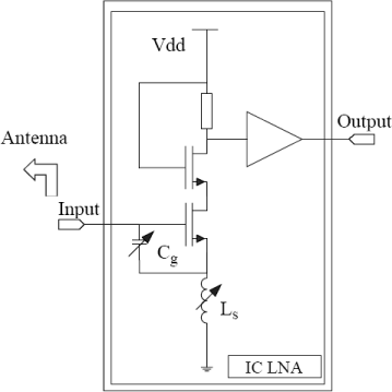
Figure 19.2. Photo of the LNA made with 0.13 μm technology in its 50 Ω version
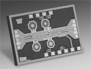
Figure 19.3. Amplifier input reactance according to Cg (Ls = 0.5 nH)
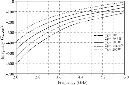
Figure 19.4. Amplifier input resistance according to Ls (Cg = 0F)
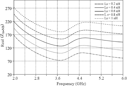
To obtain a degree of freedom making it possible to control the real part, we use the degeneration inductor parameter Ls. Figure 19.4 shows the evolution of the real part of the circuit’s input impedance according to the inductance function Ls. Using Ls means that we can control the real part efficiently: the higher the degeneration inductance the higher the resistance. We will now focus on the structure of the antenna which is the most well adapted to the LNA’s structure.
19.3. The antenna
The structure adopted for the antenna is the bow-tie dipole, selected for its wideband properties. Effectively, the slow variations in its input impedance authorize a wideband matching. The dipole arm is short-circuited in order to increase the imaginary part of its impedance, in order to display a natural conjugate behavior at the capacitive input of the amplifier’s transistors. Figures 19.5 and 19.6 show the diagram and photograph of this antenna.
Figure 19.5. Diagram showing the antenna with these two degrees of freedom
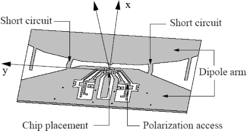
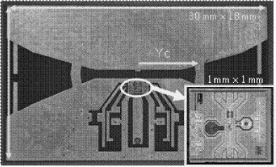
Figure 19.6. Photograph of the antenna on RO4003 substrate (30 mm × 18 mm)
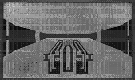
The substrate’s dielectric permittivity must not be too high, because it could become difficult to achieve a wideband adaptation. The substrate is a RO4003 type (εr = 3.38) of 0.5 mm in thickness. The radiation diagram for this antenna is omnidirectional with linear polarization [BOR 07].
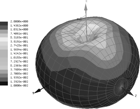
Figure 19.7. 3D simulated gain of the short-circuited monopole at 4.5 GHz ([BOR 07] © 2007, IEEE)
With regard to the antenna, co-designing may contribute to its miniaturization. Effectively, the size of the antenna is generally given by the impedance matching with its feed line. The antennas work around the resonance frequencies in order to display real impedance which is adapted to the feed line. The co-design may contribute to miniaturizing the antennas, in the sense that it might make them work at a lower frequency than the resonance, by ensuring complex conjugate matching if necessary. The position Yc of the short-circuit in relation to the center of the antenna is the main degree of freedom offered by the structure to control its impedance.
Figurea 19.8 and 19.9 show the evolution of the real and imaginary parts of the antenna’s impedance input according to the parameter Yc.
Figure 19.8. Influence of Yc over the real part Zg
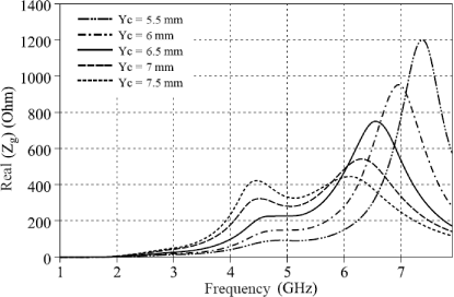
Figure 19.9. Influence of Yc over the imaginary part Zg
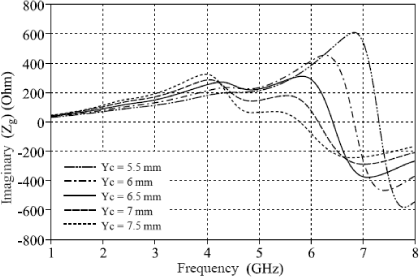
Yc is a parameter allows us to control the antenna’s specified frequency band resonance and amplitude. When we move the short-circuits away from the feeder, we increase the imaginary part of the impedance in the band [3.5 GHz — 4.5 GHz]. However, the real part also increases and may reach levels which are unacceptable for the LNA. A particularly interesting phenomenon may be seen in Figure 19.9. For a Yc value of 7.5 mm, we observe a decrease of around 4 GHz in the imaginary part. This singular evolution is symmetrical regarding the amplifier’s input reactance. It is, then, particularly interesting. These parameters, as well as the antenna’s other geometric parameters, will be adjusted in co-simulation between the antenna and the LNA.
19.4. Co-design methodology
19.4.1. Introduction
The co-design procedure follows many steps. The first step consists of assessing the maximum unilateral transducer gain GTumax which can be reached when we modify the different degrees of freedom with regard to LNA. Once this maximum level has been determined, we then need to find the antenna’s parameter Yc which enables us to present the complex conjugate value to the S11 of the active circuit input in order to fulfill matching conditions and reach this maximum transducer gain. Up until this point, the procedure is similar to that for a 50 Ω adaptation, the difference being that the amplifier’s S parameters are calculated for the input port with a complex reference impedance, that of the antenna. This perfect antenna obviously does not exist, and the co-optimization intervenes at this point. On a simulation platform which is common to both the antenna and the amplifier, we vary the antenna and the LNA’s S parameter so as to fulfill a matching condition between the two components, that highlights an as high as feasible transducer gain [PEL 06, BOR 07]. Therefore it is a matter of finding a compromise between higher maximum transducer gain and an optimum adaptation making it possible to reach this said gain.
19.4.2. Concept of transducer gain
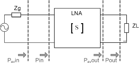
When fed into the amplifier (input), the antenna picks up radiated power in the environment and presents the amplifier an available power Pavin. At the output, the power received by the electronic load is Pout. The ratio between these two powers corresponds to the transducer gain. Figure 19.10 illustrates these powers.
Taking into account the excellent input/output isolation of the amplifier linked to the cascode stage used in LNA topology, we may consider the circuit to be unilateral. In this case, the gain is given by the following relation:
[19.1] 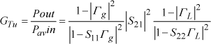
Figure 19.10. Diagram showing the different powers around the amplifier
If we consider an output load which is perfectly adapted to the measurement port Z0, then there is no output reflection (ГL= 0) and the transducer gain is written as:
[19.2] 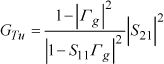
If we presume that we have a complex matching between the amplifier and the generator’s impedance ![]() , then the transducer gain is at its maximum and we then obtain the following value:
, then the transducer gain is at its maximum and we then obtain the following value:
[19.3] ![]()
Traditionally, S parameters are given with a reference impedance Z0 of 50 Ω and the impedance of antenna Zg is 50 Ω. In order to reach the transducer gain expressed in [19.3], we will introduce a passive matching network which will allow us to transform the input impedance of the circuit defined by S11 into the complex conjugate of the generator impedance Zg,. When the adaptation is carried out, ![]() is cancelled and the
is cancelled and the ![]() from the {LNA-adaptation-network}set corresponds to the maximum transducer gain from the amplifier alone.
from the {LNA-adaptation-network}set corresponds to the maximum transducer gain from the amplifier alone.
19.4.3. Variation of the circuit transducer gain
In the framework of the co-design approach, the impedance of antenna Zg may be different from 50 Ω. From the LNA perspective, S parameters vary according to the design parameters. The next step of the co-design approach consists of assessing the maximum transducer gain GTumax which can be obtained when we vary the two parameters Cg and the LNA’s degeneration inductance Ls. The investigation of the influence of these two parameters on the maximum transducer gain enables us to understand the compromises which need to be made between adaptation and gain in the co-design process.
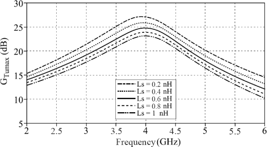
A high value of Ls makes it possible to achieve a high resistance antenna (Figure 19.4). However, we notice in Figure 19.11 a degradation in GTumax when Ls increases. Effectively, a high degeneration of the transistor reduces the amplification gain since the ratio between the drain and the source load of the LNA active transistor decreases.
Figure 19.11. Variation in GTUmax according to Ls (Cg = 0)
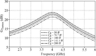
The MOS transistor input is capacitive by nature. Therefore it seems a good idea to choose an inductive antenna in order to fulfill complex matching requirements. However, the reactance of such an antenna is limited. In order to satisfy this constraint, we look to increase the value of capacitance Cg (Figure 19.4). However, increasing Cg will decrease the transducer gain, as we can see in Figure 19.12.
The maximum transducer gain GTumax evolves in a decreasing monotonic way when we increase Cg and Ls. We can reach the maximum for GTumax when there is no parallel degeneration or capacitance. The maximum value is 28.8 dB at 4 GHz. This value corresponds to the maximum transducer gain possible when we are not under any adaptation constraints.
Figure 19.12. Variation of GTUmax as a function of Cg (Ls = 0.5 nH)
19.4.4. Implementing joint optimization
Figure 19.13. Implementing co-simulation
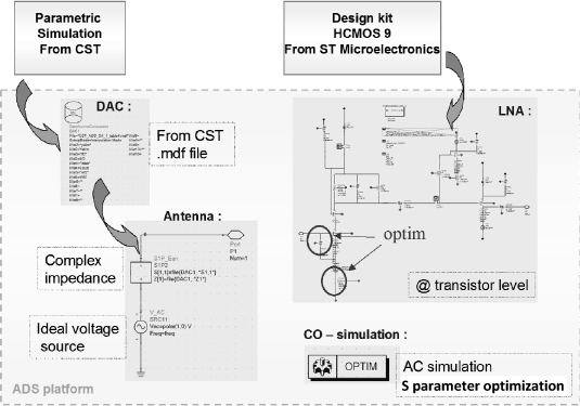
In order to co-optimize the antenna and the LNA, a common simulation platform has been developed based on ADS® software. The antenna is modeled by an ideal voltage generator in series with complex impedance. Parametric simulations using CST Microwave studio® are performed in order to generate a Data Access Component block which can be used with ADS, where the set of complex parametric impedances are put together. With regard to LNA, AC simulations are run using the design kit provided by the founder, ST Microelectronics. The co-simulation is performed in AC mode and the optimization is achieved on generalized S parameters, which are calculated with complex reference impedance.
19.5. Protocols and measurement results
Figures 19.14 and 19.15 show photographs of the prototypes made in a 50 Ω version and a version using the co-design approach.
Figure 19.14. LNA-antenna, prototypes in 50 Ω (left) and joint design (right) ([BOR 07] © 2007, IEEE)
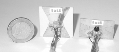
Figure 19.15. Photograph showing the association between antenna and LNA ([BOR 07] © 2007, IEEE)
As soon as the LNA is connected to the antenna, the {antenna-LNA} couple is inseparable, and characterizing the gain of this set requires us to measure the received field, which is carried out in an anechoic chamber. Thereafter, the classic methods of measuring (with two ports) the gain and the LNA’s noise factor are no longer suitable.
To be independent from the antenna’s intrinsic gain which is linked to its own radiation properties rather than the result of our co-optimization, we subtract the value of this transducer gain from the measured {antenna-LNA} pair. To determine the antenna’s intrinsic gain, it is sufficient to characterize the antenna alone in the same way as that chosen for the {antenna-LNA} pair.
We verify that in both cases, there is a conservation of the radiation diagram and we take a mean calculated over around ten angles. This measurement protocol has been followed both for the 50 Ω version and for the co-designed version. One difficulty of this protocol was accurately measuring the co-designed antenna’s gain on a traditional 50 Ω line. The RF and DC polarization cables are positioned in a way so as to avoid coupling with the radiating structure as much as possible.
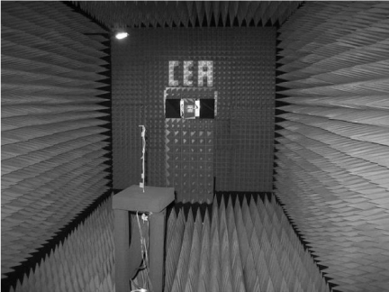
Figure 19.16 shows the characterization of the antenna associated with the LNA in an anechoic chamber.
Figure 19.16. Measuring the co-designed antenna in an anechoic chamber ([BOR 07] © 2007, IEEE)
The noise characterization in Figure 19.19 is achieved by a direct method [BOU 09, WOE 99]. This method relies on the a priori knowledge of the gain of the device (determined in the first protocol), and the antenna noise temperature which is assimilated to be the temperature in the anechoic chamber.
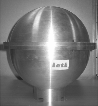
Insofar as the noise factor is a global concept which is independent of the direction of the observation, the antenna’s efficiency was determined by using the Wheeler sphere method (Figure 19.17). Measuring the noise factor remains nevertheless very tricky and is tightly linked to the gain value considered in the direct method used [BOU 09].
Figure 19.17. Wheeler sphere used for characterizing the noise factor
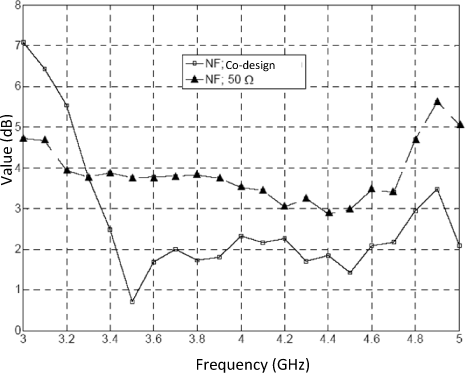
The comparison of these two approaches in terms of gain and noise factor is proposed in Figure 19.18 (gain) and Figure 19.19 (noise factor). As a result the global average gain is increased by more than 3 dB. Moreover, the bandwidth enhances by close to 15%. Eliminating passive components demonstrates that we achieved reduction of the noise factor by close to 1 dB on average over the bandwidth.
Moreover, this methodology enabled us to save 20% on the size of the chip and to miniaturize the antenna with a size reduction in the order of 30%.
Figure 19.18. Transducer gain comparison between the 50 Ω version and the co-design version
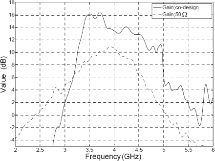
Figure 19.19. Transducer gain comparison between the 50 Ω version and the co-design version
19.6. Bibliography
[BEL 04] BEVILACQUA A., NIKNEJAD A.M., “An ultra-wideband CMOS LNA for 3.1 to 10.6 GHz wireless receivers”, IEEE Solid-State Circuits Conference, ISSCC, San Francisco, USA, February 2004.
[BOR 07] BORIES S., PELISSIER M., DELAVEAUD C., BOURTOUTIAN R., “Performances analysis of LNA-antenna co-design for UWb system”, The Second European Conference on Antennas and Propagation, EuCAP, Edinburgh, UK, November 2007.
[BOU 09] BOURTOUTIAN R., Objects communicants: miniaturisation des frontaux RF par coconception, PhD Thesis, University of Nantes, April 2009.
[PEL 06] PELISSIER M., Développements d’architecture et de fonctions RF avancées pour la réception de signaux ultra large bande dans les applications à basse consommation, PhD Thesis, Institut national polytechnique de Grenoble, November 2006.
[SHA 97] SHAEFFER D.K., LEE T.H., “A 1.5V, 1.5GHz CMOS low noise amplifier”, IEEE Journal Solid-State Circuits, vol. 32, no. 5, pp. 745–759, May 1997.
[WOE 99] WOESTENBURG E.E.M., WITVERS R.H., “Design and characterisation of a low noise active antenna (LNAA) for SKA”, Perspectives on Radio Astronomy: Technologies for Large Antenna Arrays, pp. 183–189, Astron, Dwingeloo, The Netherlands, April 1999.
1 Chapter written by Michaël PELISSIER, Serge BORIES, Raffi BOURTOUTIAN and Christophe DELAVEAUD.