
The small size of the STM32 makes it a natural application for remote control flying models. Using existing radio controllers, the STM32 could interface with receivers of RC servo signals and perform some special control features from your own imagination.
This chapter includes a demo program that uses Timer 4 to measure an incoming RC servo signal. Because the timer peripheral is doing all the work, the CPU is free to react to the servo readings with more computing power.
The Servo Signal
There is no standard for an RC servo signal, but most seem to use a pulse width of about 0.9 ms at one extreme and about 2.1 ms at the other. The repetition rate is often near 50 Hz, but can be as high as 300 Hz, depending upon manufacturer. Figure 17-1 illustrates the assumed signal that this chapter’s demo code will decode.
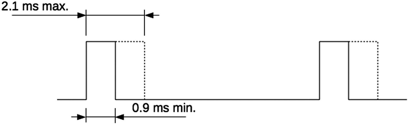
Figure 17-1 Typical RC servo signal
Positioning of the servo is governed by the width of the pulse—not the duty cycle. Because of this, some argue that this should not be called PWM (Pulse Width Modulation) at all. The mid-position of the servo is likely to be a pulse 1.5 ms wide.
Signal Voltage
The demo program uses Timer 4, which naturally has its channel 2 on GPIO PB6. This GPIO is 5-volt tolerant. Most servo signal voltages can vary from 4.5 to 6 volts. Use a 2-kohm resistor between the receiver and PB6 to safety limit the current flow. If there is a signal conflict or if the signal rises slightly above 5 volts, the resistor will limit the current to the safe amount of 0.5 mA.
Demo Project
The source code for this project is found here:
$ cd ~/stm32f103c8t6/rtos/tim4_pwm_inNow, let’s examine the demo software.
GPIO Configuration
The PB6 configuration is pretty routine. Line 45 enables GPIOB’s clock, and the remaining lines configure PB6 as an input. Even though this input is going into Timer 4, inputs never need to be declared as an alternate GPIO.
0045:   // PB6 == TIM4.CH1
0046:   rcc_periph_clock_enable(RCC_GPIOB);  // Need GPIOB clock
0047:   gpio_set_mode(GPIOB,GPIO_MODE_INPUT, // Input
0048:       GPIO_CNF_INPUT_FLOAT,GPIO6);     // PB6=TIM4.CH1
Timer 4 Configuration
Like the GPIO, the clock for Timer 4 must be enabled:
0043: rcc_periph_clock_enable(RCC_TIM4); // Need TIM4 clockNext comes the configuration of the timer itself, shown in Listing 17-1.
Listing 17-1 The Configuration of Timer 4
0050:   // TIM4:
0051:   timer_disable_counter(TIM4);
0052:   timer_reset(TIM4);
0053:   nvic_set_priority(NVIC_DMA1_CHANNEL3_IRQ,2);
0054:   nvic_enable_irq(NVIC_TIM4_IRQ);
0055:   timer_set_mode(TIM4,
0056:       TIM_CR1_CKD_CK_INT,
0057:       TIM_CR1_CMS_EDGE,
0058:       TIM_CR1_DIR_UP);
0059:   timer_set_prescaler(TIM4,72);
0060:   timer_ic_set_input(TIM4,TIM_IC1,TIM_IC_IN_TI1);
0061:   timer_ic_set_input(TIM4,TIM_IC2,TIM_IC_IN_TI1);
0062:   timer_ic_set_filter(TIM4,TIM_IC_IN_TI1,TIM_IC_CK_INT_N_2);
0063:   timer_ic_set_prescaler(TIM4,TIM_IC1,TIM_IC_PSC_OFF);
0064:   timer_slave_set_mode(TIM4,TIM_SMCR_SMS_RM);
0065:   timer_slave_set_trigger(TIM4,TIM_SMCR_TS_TI1FP1);
0066:   TIM_CCER(TIM4) &= ~(TIM_CCER_CC2P|TIM_CCER_CC2E
0067:       |TIM_CCER_CC1P|TIM_CCER_CC1E);
0068:   TIM_CCER(TIM4) |= TIM_CCER_CC2P|TIM_CCER_CC2E|TIM_CCER_CC1E;
0069:   timer_ic_enable(TIM4,TIM_IC1);
0070:   timer_ic_enable(TIM4,TIM_IC2);
0071:   timer_enable_irq(TIM4,TIM_DIER_CC1IE|TIM_DIER_CC2IE);
0072:   timer_enable_counter(TIM4);
The counter is disabled and reset in lines 51 and 52. Many of the timer’s configuration items cannot be changed when it is active. Lines 53 and 54 simply prepare for the Timer 4 interrupts.
The call of line 55 establishes the main elements of TIM4:
The input to the timer prescaler will be the internal clock.
The events within the timer will be edge driven.
The counter will count up.
Line 59 sets the timer’s prescaler to 72 so that one clock pulse will occur each microsecond. Recall that the APB1 bus is limited to 36 MHz; therefore, the APB1 prescaler divides by 2 (SYSCLK is 72 MHz). But because the APB1 prescaler is not 1, the timer global prescaler input is the APB1 bus frequency times 2, or 72 MHz.
Lines 60 and 61 indicate that timer inputs IC1 and IC2 are both being directed to timer input 1 (TI1). This fancy bit of configuration means that we can sample the servo signal with a single GPIO (PB6) but use two differently handled inputs to the timer.
Line 62 establishes a digital input filter that samples the internal clock signal (after timer’s private prescaler) divided by two. Line 63 says that the digital filter clock will have no prescaling.
Line 64 specifies that when the PB6 input rises (TI1) the counter should be cleared. The clear happens after register TIM4_CCR1 is loaded with the counter’s captured value. In this demo, this will be a measure of how long the repeat cycle is.
Line 65 sets the second trigger for Timer 2, causing the timer’s current count to be copied to capture register TIM4_CCR2. This happens when the input signal on PB6 falls back to low and thus will measure the time of the pulse width in counter ticks. This signal-change detection is based upon the digitally filtered signal from TI1.
Lines 66 through 68 configure two capture configurations:
Capture input 1 is enabled (TIM_CCER_CC1E), and
Capture input 1 is active high (default), and
Capture input 2 is enabled (TIM_CCER_CC2E), and
Capture input 2 is active low (TIM_CCER_CC2P).
Unfortunately, there are no libopencm3 routines for this at this time, so macro names were used.
Lines 69 and 70 enable the two Timer 4 inputs, and line 71 enables the Timer 4 interrupts for inputs 1 and 2. Finally, line 72 starts the Timer 4 counter.
Task1 Loop
With the timer running, our task enters a loop, which is shown in Listing 17-2. The loop runs leisurely, napping for about a second at line 75. It then toggles the LED on PC13 (as a sign of life).
Listing 17-2 The task1 Demo Loop
0019: static volatile uint32_t cc1if = 0, cc2if = 0,
0020:   c1count = 0, c2count = 0;
...
0074:   for (;;) {
0075:       vTaskDelay(1000);
0076:       gpio_toggle(GPIOC,GPIO13);
0077:
0078:       std_printf("cc1if=%u (%u), cc2if=%u (%u)
",
0079:           (unsigned)cc1if,(unsigned)c1count,
0080:           (unsigned)cc2if,(unsigned)c2count);
0081:   }
Lines 78 through 80 report some values of interest:
CC1IF is the counter value at the end of the cycle, which comes from register TIM4_CCR1. This tells us how long the cycle was in counter ticks. The value displayed in brackets after it is simply the number of times the ISR routine was entered so far.
CC2IF is the counter value captured when the input signal fell from high to low. This represents the pulse width in counter ticks. The value following in brackets is the ISR count so far.
ISR Routine
The values used by the main loop are updated by the timer’s ISR , which is shown in Listing 17-3.
Listing 17-3 The Timer ISR Routine
0022: void
0023: tim4_isr(void) {
0024:   uint32_t sr = TIM_SR(TIM4);
0025:
0026:   if ( sr & TIM_SR_CC1IF ) {
0027:       cc1if = TIM_CCR1(TIM4);
0028:       ++c1count;
0029:       timer_clear_flag(TIM4,TIM_SR_CC1IF);
0030:   }
0031:   if ( sr & TIM_SR_CC2IF ) {
0032:       cc2if = TIM_CCR2(TIM4);
0033:       ++c2count;
0034:       timer_clear_flag(TIM4,TIM_SR_CC2IF);
0035:   }
0036: }
The ISR has been enabled for input capture 1 and input capture 2 (lines 69 and 70 of Listing 17-1). When the routine is entered, the timer-status register is read in line 24. If the interrupt is due to the capture 1 event, then flag TIM_SR_CC1IF will be set (line 26). When this is true, the count is captured in line 27 and the interrupt reset in line 29. Line 28 just increments an ISR counter for printing by the main loop.
If the ISR was entered for input capture 2, then the code is similarly executed in lines 32 to 34. The values cc1if, c1count, cc2if, and c2count are the values captured and reported by the main loop (lines 78 to 80 of Listing 17-2). Note that these variables are declared with the volatile attribute because different threads of control are updating/reading these values.
Demonstration Run
The demonstration consists of hooking up the servo remote control receiver to input GPIO PB6, which is +5-volt tolerant, flashing the code, and running minicom over USB.
First, prepare the software:
$ make clobber
$ make
$ make flash
Once the software is ready in the MCU flash, it is time to hook up the RC servo receiver. Figure 17-2 illustrates the hookup.
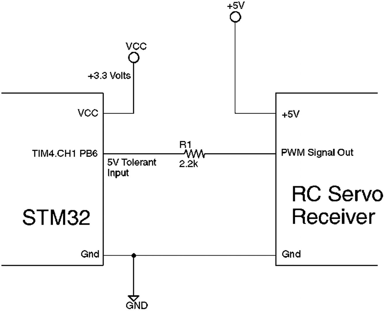
Figure 17-2 RC servo receiver hookup to STM32
Resistor R1 is highly recommended for protection. If for some reason there is a signal conflict, the resistor will limit the current flow to a safe value (3 mA or less). The GPIO input is voltage sensitive, so the resistor won’t degrade the signal.
When ready to run, plug the USB cable in and start minicom. I saved my USB settings in a file named “usb” (yours may differ):
$ minicom usbWelcome to minicom 2.7OPTIONS:Compiled on Sep 17 2016, 05:53:15.Port /dev/cu.usbmodemWGDEM1, 19:54:45Press Meta-Z for help on special keyscc1if=25174 (176), cc2if=985 (176)cc1if=25119 (215), cc2if=989 (215)cc1if=25125 (255), cc2if=974 (255)cc1if=25172 (294), cc2if=990 (294)cc1if=25134 (333), cc2if=985 (333)cc1if=25183 (372), cc2if=981 (372)cc1if=25200 (411), cc2if=992 (411)cc1if=25149 (450), cc2if=990 (450)cc1if=25339 (489), cc2if=990 (489)cc1if=24513 (528), cc2if=442 (528)cc1if=24180 (569), cc2if=209 (569)cc1if=24135 (610), cc2if=219 (610)cc1if=24283 (650), cc2if=217 (650)cc1if=24320 (691), cc2if=208 (691)cc1if=24265 (732), cc2if=258 (732)cc1if=25344 (771), cc2if=1027 (771)cc1if=26232 (809), cc2if=1698 (809)cc1if=26354 (847), cc2if=1800 (847)cc1if=26403 (884), cc2if=1871 (884)cc1if=26495 (921), cc2if=1869 (921)cc1if=26640 (959), cc2if=1887 (959)cc1if=26464 (996), cc2if=1896 (996)cc1if=26489 (1033), cc2if=1868 (1033)cc1if=26432 (1070), cc2if=1878 (1070)cc1if=26648 (1107), cc2if=1900 (1107)cc1if=26431 (1144), cc2if=1883 (1144)cc1if=26654 (1181), cc2if=1891 (1181)cc1if=26571 (1219), cc2if=1880 (1218)cc1if=26566 (1256), cc2if=1889 (1256)cc1if=26621 (1293), cc2if=1880 (1293)cc1if=26739 (1330), cc2if=1897 (1330)
Session Output
The session output consists of a one-second update of the timer values read. For example, the first line is shown here:
cc1if=25174 (176), cc2if=985 (176)The first value shown is the period of the signal. Since the timer is sampling at 1 MHz, this represents a time of:
![]()
From this figure, we can compute the period of the signal as follows:
![]()
The value (176) is the ISR counter value, which is helpful when debugging. This tells us that the ISR was entered 176 times for a timer capture 1 event.
The second value, 985, gives us the pulse width:
![]()
Later on, when the position is changed, we get:
cc1if=26739 (1330), cc2if=1897 (1330)This represents a pulse width as follows:
![]()
Timer Inputs
The demonstration illustrated how to accomplish reading the servo receiver, but how did the timer actually accomplish this? Let’s clear up the “smoke and mirrors” presentation and examine the inner workings of the input channels.
Take a moment to study Figure 17-3. This presents a somewhat simplified view of the Timer 4 inputs used. Timer 4 has a total of four inputs, but only inputs TI1 and TI2 can be used in this mode of operation.
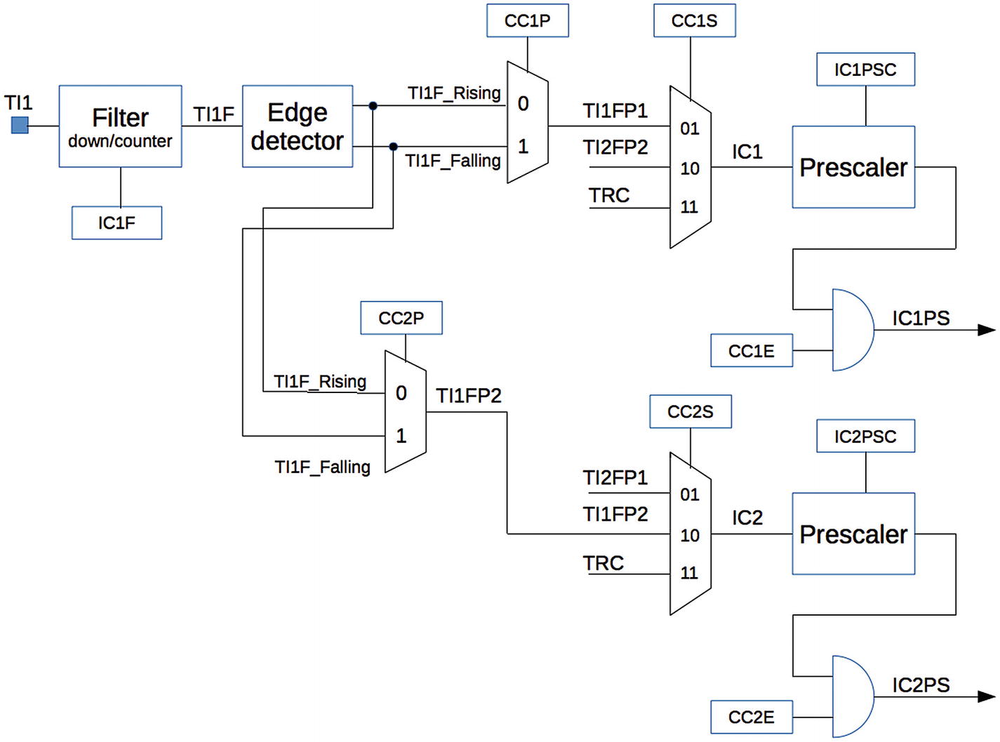
Figure 17-3 Timer input configuration
The input signal for the demo enters at TI1 from GPIO PB6. This is timer input channel 1.
TI1 is optionally conditioned by a digital filter controlled by configuration bit IC1F. The value IC1F represents a configuration item that is part of a STM32 timer register set. In this case, it is a four-bit value in register TIM4_CCMR1. Line 62 of Listing 17-1 sets this value so that the timer’s filter counter is 2. Since the clock rate f CK_INT = 1 MHz, this means that the sampled signal must be stable for two samples before the change appears after the filter at TI1F. This prevents a spurious noise pulse from triggering the timer and spoiling the reading.
Signal TI1F enters an edge detector, producing internal signals TI1F_Rising and TI1F_Falling. Configuration item CC1P chooses which signal polarity to use. Line 60 configures CC1S so that signal TI1FP1 (rising) is used as the input capture signal IC1. When this signal fires (through IC1PS), the timer’s counter is copied into the capture 1 register. Line 64 configures the timer such that the timer’s counter is reset after the capture takes place.
Input signal IC1 can be prescaled, then configured by IC1PSC. Line 63 disabled this optional feature so that there is no prescaling. Lines 68 and 69 enable CC1E, allowing the signal IC1PS to activate the capture 1 event. This particular capture measures the period of the PWM signal in the demo.
But we’re not done yet.
The configuration uses input channel 2 (IC2), derived from the signal sampled by channel 1. Configuration item CC2S in this mode causes the TI1F_Rising or TI1F_Falling (channel 1) signal to be used instead of the normal TI2 input. This is useful when measuring PWM input because we need to capture different events from the same signal. The remainder of the I2CPS chain is otherwise the same as for I1CPS, except that it drives the capture 2 event. Because IC2 is the opposite polarity (falling edge) arranged by CC2S, I2CPS can cause the capture of the counter when the signal falls. This gives us the counter at the point at which the pulse width returns to low.
Summary
This chapter demonstrated how the STM32 timer can be used to effortlessly measure the pulse width and period of a signal. In the demo, only 39 x 2 interrupts were executed to capture the period and pulse width every second. The ISR code is quite minimal, leaving valuable CPU cycles available to perform other useful work.
There are many other timer-input features that remain unexplored. The reader is encouraged to scour the STM32 reference manual RM0008 for more ideas.