1
Analog, ESD, and EOS
In 1993, I was invited to consult for two days with a well-known semiconductor analog corporation on electrostatic discharge (ESD) protection of analog components. A vice president of the corporation sat with me and said, “Our analog products are superior to any of our competitors. As a result, no one cared about the level of our ESD protection results! All of our products did not achieve 2000 V HBM or 4000 V HBM levels. Today, with growth of competition in the analog business sector, overnight, 75% of our customers want us to achieve better than 2000 V HBM levels on all of our products! How do I build a corporate ESD strategy for this analog corporation ?…”
This was my first introduction to the world of ESD in analog design.
1.1 ESD in Analog Design
In every technology sector, electrostatic discharge (ESD) protection was not an issue when there was a sole supplier of critical products and the customer was willing to accept the product. Eventually, as the technology or application space matured, customers wanted better ESD protection as both technology and application became mainstream or high volume. This was true historically in digital and analog applications with CMOS, bipolar, silicon on insulator (SOI), silicon germanium (SiGe), and gallium arsenide (GaAs) technologies. With mainstream introduction of a technology, it is desirable not to have customer field returns from ESD or electrical overstress (EOS).
As a result of the unique needs of analog design, there are a significant number of issues to be addressed in analog ESD design. These issues extend from chip design to system-level design in both architecture and layout, which consist of the following:
- Matching and layout issues
- Matching requirements in differential receivers
- Domain-to-domain separation and ESD coupling
- Circuit topology chip architecture and ESD
- Interdomain digital-to-analog ESD failures
- Semiconductor chip layout floor planning
- Printed circuit board (PCB) design floor planning
- High-voltage applications
- Ultrahigh-voltage applications
In this text, examples will be provided of ESD failures and problems in past analog applications to modern-day practices in analog design. The text will discuss how the present-day architecture of mixed-signal chips evolved and its implications.
1.2 Analog Design Discipline and ESD Circuit Techniques
In analog design, unique design practices are used to improve the functional characteristics of analog circuitry [1–10]. In the ESD design synthesis of analog circuitry, the ESD design practices must be suitable and consistent with the needs and requirements of analog circuitry [11, 12] (Figure 1.1). Fortunately, many of the analog design practices are aligned with ESD design practices.

Figure 1.1 Analog and ESD design.
In the analog design discipline, there are many design techniques to improve tolerance of analog circuits [10]. Analog design techniques include the following:
- Local matching: Placement of elements close together for improved tolerance
- Global matching: Placement in the semiconductor die
- Thermal symmetry: Design symmetry
A key analog circuit design requirement is matching. To avoid semiconductor process variations, matching is optimized by the local placement. Placement within the die location also is an analog concern due to mechanical stress effects. In analog design, there is a concern of the temperature field within the die and the effect of temperature distribution within the die.
Many of the analog design synthesis and practices are also good ESD design practices. The design practices of matching and design symmetry are also suitable practices for ESD design. But there are some design practices where a trade-off exists between the analog tolerance and ESD; this occurs when parasitic devices are formed between the different analog elements within a given circuit or circuit to circuit.
1.2.1 Analog Design: Local Matching
Matching is important in analog design due to the usage of many circuit blocks that require good matching characteristics. The matching is important locally in a semiconductor device or within a circuit. In this case, “local matching” is needed to provide the ideal characteristics of an analog network. Local matching is critical in multifinger structures, where mismatch can occur between two adjacent structures. In future sections, discussion of semiconductor processes such as photolithography and etching influences the local matching.
1.2.2 Analog Design: Global Matching
Matching is important in analog design due to the usage of many circuit blocks that require good matching characteristics from circuit to circuit. Many functional analog circuit blocks are repeated within a semiconductor chip. In this case, “global matching” is needed to avoid mismatch between two circuits. Global matching is influenced by spatial separation of two circuits, global density variations, arrangement, and orientation. Global matching is influenced by across chip linewidth variation (ACLV).
1.2.3 Symmetry
Symmetry is critical to establish matching within a semiconductor device or an analog circuit (Figure 1.2). Symmetry is influenced by design layout, current distribution, temperature field, and thermal distribution [10].

Figure 1.2 Symmetry and layout.
1.2.3.1 Layout Symmetry
Layout symmetry is a form of symmetry through physical design. Layout symmetry establishes matching within a semiconductor device or an analog circuit [10].
1.2.3.2 Thermal Symmetry
Thermal symmetry is a form of symmetry through the temperature field and thermal distribution. Thermal symmetry establishes matching within a semiconductor device or an analog circuit [10].
1.2.4 Analog Design: Across Chip Linewidth Variation
In semiconductor development, semiconductor process variation can introduce structural and dimensional nonuniformity which influences both analog circuits and ESD devices [13–22]. Photolithography and etch tools can introduce these nonuniformities that exist on a local and global design level. These variations can manifest themselves by introducing variations in both active and passive elements. For MOSFET transistors, variation in the MOSFET channel length in single-finger and multifinger MOSFET layouts can lead to nonuniform “turn-on”; this effect can influence both active functional circuits and ESD networks. In bipolar transistors, the linewidth variation can lead to different sizes in emitter structures, leading to nonuniform current distribution in multifinger bipolar transistors. For resistor elements, resistor elements that are utilized for ballasting in multifinger structures can also lead to nonuniform current in the different fingers in the structure.
Design factors that influence the lack of variation are the following semiconductor process and design variables:
- Linewidth
- Line-to-line space
- “Nested-to-isolated” ratio
- Orientation
- Physical spacing between identical circuits
It is a circuit design practice and an ESD design synthesis practice to provide a linewidth which is well controlled. For line-to-line space, in an array of lines, the spacing is maintained to provide maximum matching between adjacent lines. For example, in a multifinger MOSFET structure, the spacing between the polysilicon lines is equal to provide the maximum matched characteristics.
Given any array of parallel lines, the characteristics of the “end” or edges of the array can have different characteristics than the other lines. In an array of lines, whereas one edge is adjacent to another line, the other edge is not; this leads to one line-to-line edge space to appear “nested” and the outside line-to-line edge space to appear “semi-infinite” or “isolated.” To address the problem of poorly matched edge lines, the following semiconductor process and ESD design solutions are used:
- Process: Cancellation technique of photolithography and etch biases
- Design: Use of dummy edge lines
- Circuit: Use of “gate-driven” circuitry
Orientation can also influence the linewidth of identical circuits both locally and globally. An ESD design practice is to maintain the same x–y orientation of ESD circuits in a semiconductor chip to minimize variation pin to pin. This is not always possible in a peripheral architecture where the ESD element is rotated on the four edges of the semiconductor chip. Note that in this case, the circuit itself (e.g., off-chip driver) may also undergo an orientation effect. It is a good ESD design synthesis practice that addresses the orientation issue with compensation and matching issues for orientation of the ESD elements (in conjunction with the circuit it is protecting).
On a macroscopic full-chip scale, variations in the photolithography and etching can vary from the top to bottom of a semiconductor chip. In the design of a semiconductor chip, these can be compensated with a preknowledge of the photolithography and etch variations of a technology.
1.3 Design Symmetry and ESD
Design symmetry is an ESD design practice to maximize the ESD robustness [23]. The capability of the ESD network to dissipate high-current pulse events is directly related to the network’s topology and its design symmetry. The more uniform the current distribution is through the ESD network during a discharge, the better the utilization of the area of the structure, and as a consequence, the greater the robustness of the circuit design. The distribution of current during an ESD event is dependent upon the design symmetry of the ESD network and its components.
From experience, to the degree that the design of the ESD network (or structure) on all levels of the integrated circuit (IC) departs from a symmetric configuration, the greater is the current localized or nonuniformities in the ESD network. With a symmetrical distribution of the current, the peak power-to-failure per unit area is lowered, producing superior results. Additionally, the more uniform the current distribution, the more uniform the thermal field as well. Since semiconductor element electrical and thermal parameters are temperature dependent (e.g., mobility, electrical conductivity, thermal conductivity), the more uniform the current distribution, the more symmetrical the temperature distribution within the device.
In IC design, a key ESD design concept is to maintain a high degree of design symmetry within a structure on all design levels. In both the ESD network and I/O driver circuit, an evaluation of the power distribution of an ESD event within the circuit is an indicator of the robustness of the IC. Hence, physical layout design symmetry can be used as a heuristic determination of the power distribution within a physical structure.
To evaluate ESD design symmetry, this can be done visually in a design review or through a means of an automated computer-aided design (CAD) tool [23].
ICs are produced on a uniform substrate which are the subject of numerous mask operations. The masks create from lines and shapes individual devices on the layers of the ICs. Hence, the mask physical layout features can be used to quantify the ESD design symmetry. This can be done on each of the layout design levels of the ESD structure.
To define ESD design symmetry, an axis of symmetry can be defined in the ESD design. Semiconductor design layout is two dimensional, allowing to define an axis of symmetry in the x- and y-direction. In this fashion, “moments” can be defined about the axis of symmetry as a means of quantifying the degree of symmetry and identify nonsymmetric features.
Before manufacturing the IC in silicon, the data file which defines the lines and shapes of each mask is available for evaluating the design to be implemented in silicon. In this methodology, a method can define the symmetry which evaluates on a level-by-level basis.
In this design methodology, the method provides for evaluating the degree of design symmetry of the proposed semiconductor device, by considering various topological features of the design such as the directional flow of current into and out of the device, circuit element design symmetry, metal and contact symmetry, and other design features which reduce the robustness of an ESD protection network.
The semiconductor design can be “checked” before implementing in silicon by evaluating each ESD shapes. In the event that any level fails the check, the level can be redesigned before implementing in silicon.
1.4 ESD Design Synthesis and Architecture Flow
In the ESD design synthesis process, there is a flow of steps and procedures to construct a semiconductor chip. The following design synthesis procedure is an example of an ESD design flow needed for semiconductor chip implementations [13, 14, 22]:
- I/O, domains, and core floor plan: Define floor plan of regions of cores, domains, and peripheral I/O circuitry
- I/O floor plan: Define area and placement for I/O circuitry
- ESD signal pin floor plan: Define ESD area and placement
- ESD power clamp network floor plan: Define ESD power clamp area and placement for a given domain
- ESD domain-to-domain network floor plan: Define ESD networks between the different chip domains area and placement for a given domain
- ESD signal pin network definition: Define ESD network for the I/O circuitry
- ESD power clamp network definition: Define ESD power clamp network within a power domain
- Power bus definition and placement: Define placement, bus width, and resistance requirements for the power bus
- Ground bus definition and placement: Define placement, bus width, and resistance requirements for the ground bus
- I/O to ESD guard rings: Define guard rings between I/O and ESD networks
- I/O internal guard rings: Define guard rings within the I/O circuitry
- I/O external guard rings: Define guard rings between I/O circuitry and adjacent external circuitry.
1.5 ESD Design and Noise
In semiconductor chips, the switching of circuitry can lead to noise generation that can influence circuit functions [17]. In the architecture of a semiconductor chip, different domains are separated due to noise generation. Noise is generated from undershoot and overshoot phenomena of signal leading to substrate injection. Noise can be also generated from switching of off-chip drivers circuitry and large power devices.
In a semiconductor chip, there are circuitries which are sensitive to the noise generation. To avoid noise from impacting functionality of the sensitive circuitry, separate power domains are created on a common substrate. Examples of separation of power domains and semiconductor chip functions are as follows [13, 22] (Figure 1.3):
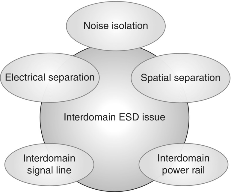
Figure 1.3 Noise and spatial separation.
- Separation of peripheral circuitry from core circuitry
- Separation of peripheral circuitry from core memory regions
- Separation of digital and analog functions
- Separation of digital, analog, and radio frequency (RF) functions
- Separation of power, digital, and analog functions
In ESD design, the separation of different circuit domains for noise isolation can lead to ESD failures. ESD failures can occur due to the following situations:
- Lack of a forward bias current path between a first power rail and a second power rail
- Lack of a forward bias current path between a pin of a first domain and a power rail of a second domain
- Lack of a forward bias current path between a pin of a first domain and a pin of a second domain
As a result, in the ESD design synthesis, the architecture of the semiconductor chip which is separated for noise must allow for current to flow from domain to domain. As a result, there is a trade-off between the noise isolation and the requirement of allowance of current flow between pins and power rails of different domains. Various means have been utilized to achieve this. Examples of solutions between independent power domains are as follows:
- Symmetric and asymmetric bidirectional ESD networks between domains of VDD(i) and VDD(j)
- Symmetric and asymmetric bidirectional ESD networks between domains of VDD(i) and VSS(j)
- Symmetric and asymmetric bidirectional ESD networks between domains of VSS(i) and VSS(j)
1.6 ESD Design Concepts: Adjacency
An ESD design concept is the issue of adjacency. In the physical layout design of ESD structures, the adjacency of structures internal and external of the ESD element is a concern.
Structures adjacent to ESD structures can lead to both ESD failure mechanisms and latchup. Adjacent structures can lead to parasitic device elements not contained within the circuit schematics. Parasitic npn, pnp, and pnpn are not uncommon in the design of ESD structures. These parasitic bipolar transistor elements can occur between the ESD structure and the guard rings around the ESD structure. These parasitic elements can occur in single-well, dual-well, and triple-well CMOS, DMOS, bipolar, BiCMOS, and BCD technologies.
1.7 Electrical Overstress
EOS is such a broad spectrum of phenomena; it is important to establish classifications of EOS [13]. The definition of EOS includes electrical response to current, voltage, and power.
Electrical phenomena are categorized into different definitions, which will be discussed in depth in further sections. Common categorization includes ESD, electromagnetic interference (EMI), electromagnetic compatibility (EMC), and latchup issues (Figure 1.4) [13, 14, 22]. At times, all of these are included in the definition of EOS; yet others separate these categories as separate items to distinguish them for the purpose of determining cause–effect relationships, as well as root cause. For example, although ESD is a form of EOS, it is established in the semiconductor industry to distinguish between ESD and EOS. One of the reasons this is done is due to determining the root cause of failure.
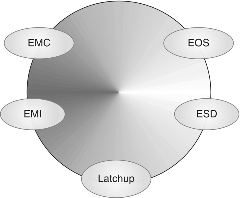
Figure 1.4 EOS, ESD, EMI, EMC, and latchup.
EOS cause and effect for ICs can be the following [13]:
- ESD
- Latchup
- EMI
- EMC
- Misapplication
For ESD phenomena, there exist event models for the component and system levels. For component-level ESD, failures can be associated with human body model (HBM), machine model (MM), charged device model (CDM), and human metal model (HMM) [13–22]. For system-level ESD, failures can be associated with charged board model (CBM) and cable discharge event (CDE) [13, 14].
For latchup, there exist causes associated with direct current (DC) and transient phenomena [18]. DC latchup events can be in the form of “internal latchup” and “external latchup.” Transient latchup is also the initiation of latchup from a transient voltage event.
For EMI, EOS events can occur from the following [13]:
- Noise
- Surge currents
- Slow voltage transients
- Fast voltage transients
- RF signals
For the EMI events, there are causes for noise, surge currents, transients, and RF interferences. Noise can be a result of lack of proper filters and switching events. Surge currents can occur due to poor electrical isolation and switching of capacitors. Voltage transients can occur due to power-up and power-down of PCB and ICs. Inductive switching is also a transient voltage concern. RF interference can be a concern from lack of filters, lack of shielding, shielding openings, and the PCB design quality [13, 14, 17].
Human error and misapplication is a large cause of EOS events. This can happen in the following forms:
- System design
- Improper testing
- Improper assembly
- Specification violation
EOS can be a result of poor system design [13]. System design can be both hardware and software. Improper or inadequate design of both the electrical and thermal properties can lead to EOS.
EOS events can be the result of improper testing [13]. Human error from incomplete tests, hot swapping, and switching of components, and inadequate margins can lead to over-voltage and over-current of applications. Overvoltage can also occur in the test equipment sources themselves due to noise, transient spikes, and other poor-quality test environments.
Improper assembly and human error can also be the cause of EOS issues. In the assembly process, misorientation, misinsertion, reverse insertion, and assembly of powered or unpowered states can lead to EOS.
In addition, electrical specifications can be violated due to defective hardware (e.g., opens and shorts), poor electrical contacts, poor ground connections, and overheating.
Throughout the text, these issues will be reemphasized, repeated, and addressed in detail. To continue with our discussion, more definitions will be established in this chapter.
1.7.1 Electrical Overcurrent
There are different forms of EOS [13]. In electrical conditions that are in excess of the intended or application current, devices, components, or systems can undergo latent or permanent damage; this condition can be defined as electrical overcurrent (EOC).
When EOC occurs, electronic components can have excessive Joule heating, material property changes, melting, or fire. EOC is one classification of EOS. EOC can be prevented by electrical fuses, temperature sensing circuitry, and current-limiting EOS protection devices.
1.7.2 Electrical Overvoltage
In electrical conditions that are in excess of the intended or application voltage, devices, components, or systems can undergo latent or permanent damage; this condition can be defined as electrical overvoltage (EOV). When EOV occurs, electronic components can undergo different conditions. EOV can lead to electrical breakdown of dielectrics, semiconductors, and conductors and is a second classification of EOS.
EOV can be prevented by voltage-limiting EOS protection devices and ESD protection circuits.
1.7.3 Electrical Overstress Events
EOS can occur within manufacturing environments and production areas and in the field [13]. EOS events can occur internal or external of electronic systems. External sources can be associated with voltage sources, current sources, and phenomena associated with inductive, capacitance, or resistive components. The phenomena can be DC, alternating current (AC), or transient phenomena.
Examples of different external sources of EOS events include the following:
- Inductance: Inductive loads
- Capacitive: Cable capacitance charge
- Resistive: Ground resistance
Electronic noise in different forms is also a key cause of EOS events. Noise events, both internal and external, can create component failures. Examples of noise events include the following:
- External switching noise: Switching noise on antennas
- External ground plane noise: Noise on ground plane or current return
- External EMI: EMI noise due to poor shielding
- Internal switching I/O noise: Sequential switching of digital I/O off-chip driver circuitry
- Internal switching clock noise: Switching of timing clocks
- Internal I/O transients: Overshoot and undershoot.
1.7.3.1 Characteristic Time Response
ESD event characteristic time response is associated with a specific process of charge accumulation and discharge. Hence, the characteristic time response is definable enough to establish an ESD standard associated with the specific process. Secondly, the time response of ESD events is fast processes. The time constant for ESD events ranges from subnanoseconds to hundreds of nanoseconds.
In contrary, EOS events do not have a characteristic time response [13]. They can have short time response or long (note: today, it is popular to separate the “ESD events” as distinct from “EOS events” which is what will be followed in this text). EOS processes are typically slower and distinguishable from ESD events by having longer characteristic times. The time constant for EOS events ranges from submicroseconds to seconds (Figure 1.5).

Figure 1.5 EOS and ESD event time constant spectrum.
1.7.4 Comparison of EOS versus ESD Waveforms
Figure 1.6 contains both examples of ESD and EOS waveforms. In the plot, ESD waveforms for the HBM, MM, and IEC 61000-4-2 are shown. In comparison, an EOS waveform is highlighted. The key point is that the ESD event waveforms are significantly shorter than EOS events.
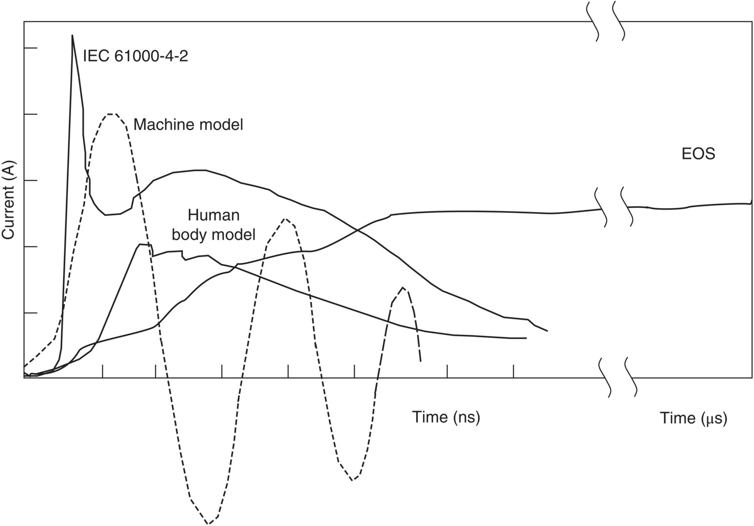
Figure 1.6 EOS and ESD event waveform comparison.
1.8 Reliability Technology Scaling and the Reliability Bathtub Curve
As technologies are scaled, the reliability of semiconductor devices is being affected [13]. This can be observed from the reliability “bathtub” curve. The reliability bathtub curve has three regimes to predict failure rate on a logarithm–logarithm plot of FITs versus time. The FIT rate is the number of fails in 1 billion hours. The first region is known as the infant mortality regime, followed by a second time regime, known as the use or useful life regime, followed by the end-of-life (EOL) regime. The infant mortality is a decreasing linear regime on a log FIT versus log time plot. The second useful life regime is time independent and a low flat FIT rate. As one approaches the EOL regime, reliability “wear-out” begins leading to a linear increase in the FIT rate (Figure 1.7).
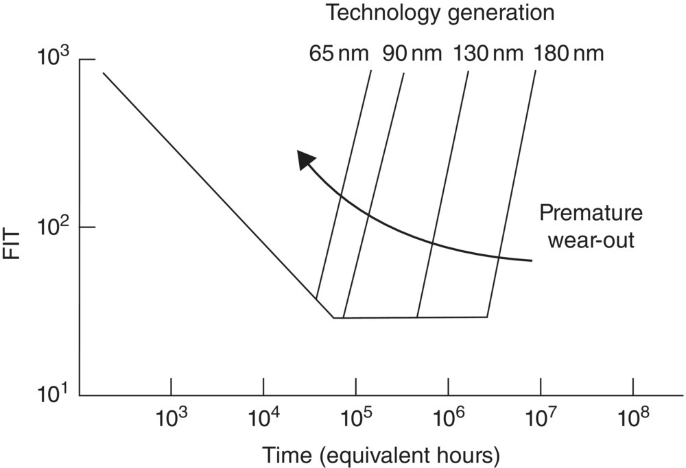
Figure 1.7 Reliability bathtub curve and technology scaling.
As technologies are scaled, premature wear-out is occurring with a continued decrease in the length of the useful life regime. As technologies are scaled from 180 nm to below 65 nm, the length of useful life is decreasing, and wear-out will be a larger issue.
This indicates that the fundamental devices within a semiconductor chip are becoming weaker with technology scaling; it will be important to improve the reliability of components by improving EOS robust circuits through layout, design, topology, and other means to counter the decreasing reliability of semiconductor devices.
1.8.1 The Shrinking Reliability Design Box
With technology scaling, the reliability design box is decreasing. Figure 1.8 shows an example of the scaling of the technology reliability design box. With each successive generation, the technologies are getting less robust from a reliability perspective. To compensate for the degradation in the technology device reliability, the solution to provide future EOS robust technology is by providing more EOS robust circuits. EOS robust circuits will be achieved through design layout and circuit topology solutions.

Figure 1.8 Shrinking technology design box.
1.8.2 Application Voltage, Trigger Voltage, and Absolute Maximum Voltage
One of the challenges in the development of EOS solution is to develop EOS protection networks whose turn-on voltage is initiated above the application voltage but below the failure voltage of the device or circuit [13]. On the voltage axis, there are an application voltage, a trigger voltage (e.g., clamp voltage) of the EOS protection device, and the absolute maximum (e.g., ABS MAX) voltage allowable on the device or circuit. Hence, there is a desired “window” on the voltage axis where the EOS protection network should operate, as illustrated in Figure 1.9. If the EOS protection voltage turn-on is below the application voltage, the EOS element is “on” during the voltage application range. If the EOS protection voltage turn-on is above the absolute maximum voltage (ABS MAX), then the circuit fails prior to initiation of the EOS protection solution.

Figure 1.9 Voltage axis highlighting application voltage, EOS protection trigger voltage, and the ABS MAX voltage.
When this occurs, the application voltage must address variations in the power supply, VDD, with a maximum application voltage of VDD + ΔVDD. This reduces the triggering window for the EOS solution. In addition, there is temperature variation that also broadens the application space. As a result, the EOS trigger window also is reduced. Hence, the EOS protection element must remain “off” during worst-case voltage and worst-case temperature conditions of the application.
For EOS solutions, another challenge is that there most likely are ESD elements in series with the EOS protection solution, which may also remain off during the application voltage, and must also turn-on below the absolute maximum voltage condition of the circuit or device. For power electronics and smart power applications, one of the challenges is to provide a solution for both EOS and ESD protection.
1.9 Safe Operating Area
Electrical devices, either in integrated electronics or discrete elements, have a region which is regarded as the safe operating area (SOA) in current–voltage (I–V) space [13, 14]. I–V points in the interior of the safe operating I–V space are regarded as states where the device is safe to operate, and I–V points outside of this (SOA) are regarded as a domain where it is regarded as unsafe.
The SOA can be defined from an electrical or thermal perspective. Additionally, one can define a DC SOA or a transient SOA.
Figure 1.10 provides an example of an SOA in the I–V space for a given device.

Figure 1.10 Safe operating area.
1.9.1 Electrical Safe Operating Area
Figure 1.11 shows an example of an SOA which includes a thermal limit. A power contour forms a hyperbola on the I-V plot since power equals the product of current times voltage (P=IV). In components and systems, the voltage and current specifications for a rectangle in the I–V space. But, due to power limitations, the upper right corner is limited by both power and thermal limits [10, 11, 13, 14].
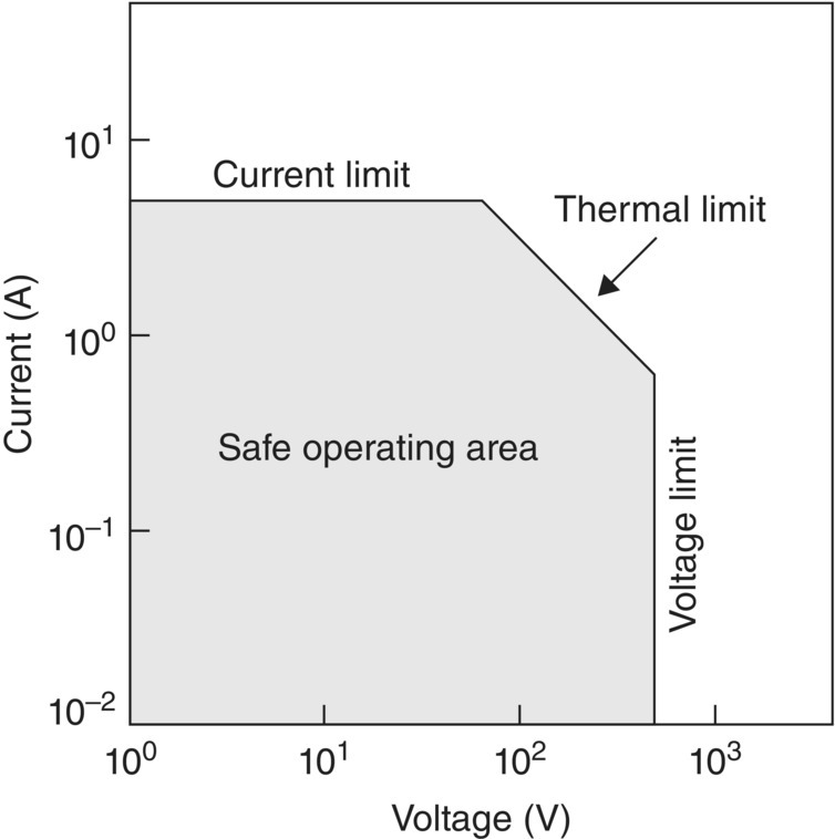
Figure 1.11 SOA with thermal limit.
1.9.2 Thermal Safe Operating Area (T-SOA)
With electronic components, there is a region for current and voltage conditions between the electrical safe operating area (E-SOA) and thermal runaway (e.g., thermal breakdown). This region can be referred to as the thermal safe operating area (T-SOA). Figure 1.12 shows the SOA with a thermal limit and second breakdown limitations. Thermal breakdown leads to failure and destruction of a component [10, 11, 13, 14].
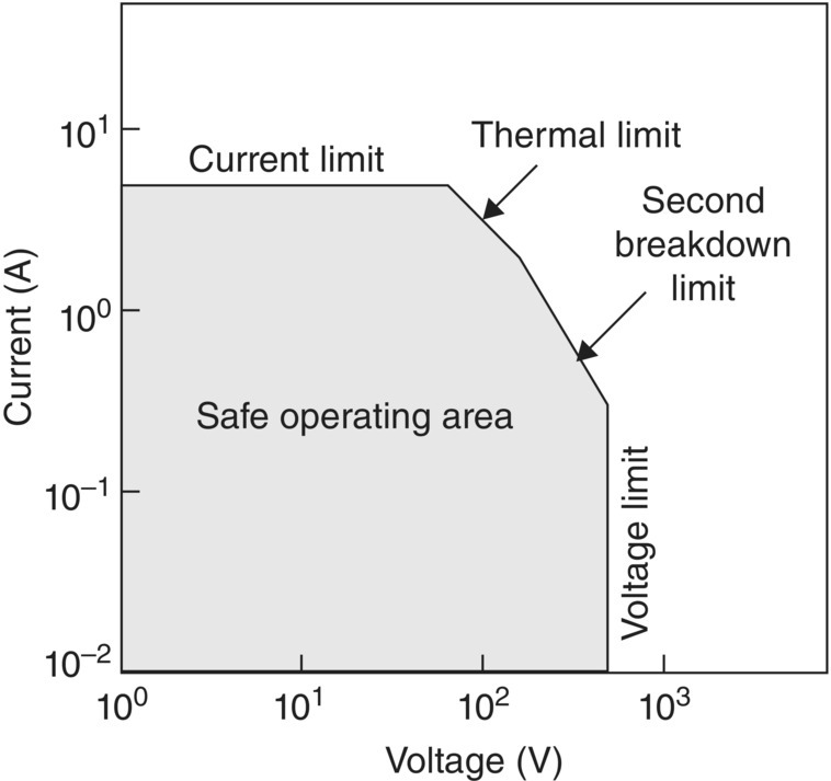
Figure 1.12 SOA with thermal limit and second breakdown limit.
In the T-SOA, permanent degradation of electrical components can occur due to excessive heating. In this regime, Joule heating can occur.
1.9.3 Transient Safe Operating Area
For EOS, transient phenomena can influence the failure level of a device or component. The quantification of the transient response can be defined by identifying and defining a “transient safe operating area.” To define the transient pulse, it can be quantified as a trapezoidal pulse as is defined in the transmission line pulse event. The trapezoidal pulse is defined with a rise time, a plateau, and a fall time. As shown in Figure 1.13, voltage states and affiliated time constants can be defined. The voltage can be defined as a plateau voltage, a peak voltage, and a “safe” voltage. For the time constants, corresponding times can be quantified, such as the unsafe transient time constant (time to the safe voltage), the peak voltage time, the safe voltage time, the quasistatic time (time to the plateau state), as well as the pulse time and the fall time [13].

Figure 1.13 Transient safe operating area voltage-time waveform.
1.10 Closing Comments and Summary
This chapter opened with the discussion of analog design principles associated with matching and design symmetry. It also discussed EOS and its relationship to other phenomena, such as ESD, EMI, EMC, and latchup. EOS is defined as well in terms of EOC, electrical overpower, and other concepts. In our discussion, there is an emphasis on ESD and EOS events on analog applications. As a result, we have drawn distinctions through the text on difference of failure analysis, time constants, and other means of identification and classification. A plan to define SOA and its role in EOS is also emphasized.
Chapter 2 discusses analog design layout practices of interdigitated design layout and common centroid concepts in one- and two dimensions. These concepts are implemented into ESD networks and the cosynthesis of analog circuits and ESD networks.
References
- 1. A.B. Glasser and G.E. Subak-Sharpe. Integrated Circuit Engineering. Reading, MA: Addison-Wesley, 1977.
- 2. A. Grebene. Bipolar and MOS Analog Integrated Circuits. New York: John Wiley & Sons, Inc., 1984.
- 3. D.J. Hamilton and W.G. Howard. Basic Integrated Circuit Engineering. New York: McGraw-Hill, 1975.
- 4. A. Alvarez. BiCMOS Technology and Applications. Norwell, MA: Kluwer Academic Publishers, 1989.
- 5. R.S. Soin, F. Maloberti, and J. Franca. Analogue-Digital ASICs, Circuit Techniques, Design Tools, and Applications. Stevenage, UK: Peter Peregrinus, 1991.
- 6. P.R. Gray and R.G. Meyer. Analysis and Design of Analog Integrated Circuits. 3rd Edition. New York: John Wiley & Sons, Inc., 1993.
- 7. F. Maloberti. Layout of analog and mixed analog-digital circuits. In: J. Franca and Y. Tsividis (Eds). Design of Analog-Digital VLSI Circuits for Telecommunication and Signal Processing. Upper Saddle River, NJ: Prentice Hall, 1994.
- 8. D.A. Johns and K. Martin. Analog Integrated Circuit Design. New York: John Wiley & Sons, Inc., 1997.
- 9. R. Geiger, P. Allen, and N. Strader. VLSI: Design Techniques for Analog and Digital Circuits. New York: McGraw-Hill, 1990.
- 10. A. Hastings. The Art of Analog Layout. Upper Saddle River, NJ: Prentice Hall, 2006.
- 11. V. Vashchenko and A. Shibkov. ESD Design for Analog Circuits. New York: Springer, 2010.
- 12. H. Kunz, G. Boselli, J. Brodsky, M. Hambardzumyan, and R. Eatmon. An automated ESD verification tool for analog design. Proceedings of the Electrical Overstress/Electrostatic Discharge (EOS/ESD) Symposium, 2010; 103–110.
- 13. S. Voldman. Electrical Overstress (EOS): Devices, Circuits, and Systems. Chichester, UK: John Wiley & Sons, Ltd, 2013.
- 14. S. Voldman. ESD Basics: From Semiconductor Manufacturing to Product Use. Chichester, UK: John Wiley & Sons, Ltd, 2012.
- 15. S. Voldman. ESD: Physics and Devices. Chichester, UK: John Wiley & Sons, Ltd, 2004.
- 16. S. Voldman. ESD: Circuits and Devices. Chichester, UK: John Wiley & Sons, Ltd, 2005.
- 17. S. Voldman. ESD: RF Circuits and Technology. Chichester, UK: John Wiley & Sons, Ltd, 2006.
- 18. S. Voldman. Latchup. Chichester, UK: John Wiley & Sons, Ltd, 2007.
- 19. S. Voldman. ESD: Circuits and Devices. Beijing: Publishing House of Electronic Industry (PHEI), 2008.
- 20. S. Voldman. ESD: Failure Mechanisms and Models. Chichester, UK: John Wiley & Sons, Ltd, 2009.
- 21. M. Mardiquan. Electrostatic Discharge: Understand, Simulate, and Fix ESD Problems. Hoboken, NJ: John Wiley & Sons, Inc., 2009.
- 22. S. Voldman. ESD: Design and Synthesis. Chichester, UK: John Wiley & Sons, Ltd, 2011.
- 23. S. Voldman. Method for evaluating circuit design for ESD electrostatic discharge robustness. U.S. Patent No. 6,526,548, February 25, 2003.
