
8
Analog and ESD Circuit Integration
8.1 Analog and Power Technology and ESD Circuit Integration
In analog circuitry and power applications, a large number of electrostatic discharge (ESD) networks are needed due to the breadth of applications, application voltages, and technology requirements [1–11]. ESD networks must be suitable for the application voltages ranging from 1.5 V to ultrahigh-voltage (UHV) conditions of 600–800 V. In this chapter, the discussion will go into greater depth on the needs of an analog and power technology, with some focus on the issues for analog power ESD networks.
8.1.1 Analog ESD: Isolated and Nonisolated Designs
In analog circuitry, the ability to isolate the network from the substrate is necessary for voltage isolation, noise, or latchup [11]. In LDMOS and bipolar-CMOS-DMOS (BCD) technology, transistor elements can be placed in the substrate or in an isolation well structure. ESD protection networks can be constructed with both isolated and nonisolated designs. For ESD designs that are isolated, the isolation voltage is the maximum voltage that the element can be used for a given power supply application voltage.
8.1.2 Integrated Body Ties
In high-voltage (HV) applications from 5 to 120 V, an important issue is whether a device has a “body tie” electrically connecting a source to the LDMOS body [11]. In some ESD networks, it may be required to not connect the transistor body to the source but have the ability to isolate them. In networks that require “stacking” of elements, it may require the electrical separation of the source and the “body” of an LDMOS transistor.
8.1.3 Self-Protecting versus Non-Self-Protecting Designs
In HV applications from 5 to 120 V, analog circuitry can be designed to be “self-protecting” without additional ESD networks [11]. For power applications, the physical width of “pull-up” and “pull-down” transistors can be very large. As a result, an ESD network may not be necessary. Self-protecting analog circuits may require specific layout practices that allow for more ESD or electrical overstress (EOS) robustness than standard LDMOS or DeMOS devices.
8.2 ESD Input Circuits
ESD protection of input circuit is critical due to the ESD sensitivity of input circuitry. Input circuits are typically small circuits. In the following sections, analog input circuits for both low voltage (LV) and HV are discussed.
8.2.1 Analog Input Circuit Protection
Analog input protection is critical due to the sensitivity of input circuitry. In addition, for power electronics, the issues of application voltages, isolation voltage, ESD “turn-on voltages,” and ESD device breakdown voltages are important to have proper cosynthesis of analog circuits and ESD devices. This section will introduce additional analog ESD networks for power devices.
8.2.2 High-Voltage Analog Input Circuit Protection
In HV applications from 5 to 120 V, HV analog inputs will require usage of ESD elements whose breakdown voltage to the isolation or substrate is above the application voltage. Whereas LV CMOS can utilize CMOS diode-based elements, this is not possible when the n-well-to-substrate breakdown voltage is below the application voltage. As a result, LDMOS transistors can be used in LDMOS and BCD technology for analog input ESD networks. Figure 8.1 shows an example of a single-stage LDMOS-based input network. The analog ESD network uses a p-channel LDMOS device between analog input and the high-voltage power supply voltage VCCHV and an n-channel LDMOS device between analog input and ground (VSS). In these circuits, the LDMOS gate breakdown voltage must be suitable for the application voltage, as well as the isolation breakdown voltage through the signal swing of the application, and relative to the power supply voltage VCCHV.

Figure 8.1 Analog input protection with LDMOS transistors.
8.2.3 Analog Input High-Voltage Grounded-Gate NMOS (GGNMOS)
In analog design, HV inputs utilize a commonly used voltage triggered ESD network, which is, which is the HV grounded-gate NMOS (GGNMOS) network. Figure 8.2 is an example of an HV GGNMOS network used for analog and power applications. For analog and power applications, the HV GGNMOS transistor must have a high dielectric breakdown voltage to avoid gate-to-drain breakdown. LDMOS transistors that have breakdown voltage tolerance are commonly used. For power applications, the GGNMOS device utilized must also have an isolation voltage above the application voltage. In many power applications, the “body” can float to avoid electrical breakdown in ESD protection networks.
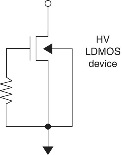
Figure 8.2 Analog input protection with LDMOS transistors.
8.2.4 Two-Stage High-Voltage Analog Input Circuit Protection
HV analog inputs will require a multistage ESD network to lower the voltage at the input pin during an ESD or EOS event. In analog design, usage of resistor elements in series with inputs is acceptable for performance- or nonperformance-based networks. Figure 8.3 shows an example of a two-stage HV analog network that contains a PDMOS element, an NDMOS element, a series resistor, and a diode element prior to the circuit. Note that this will require usage of ESD elements whose breakdown voltage to the isolation or substrate is above the application voltage.
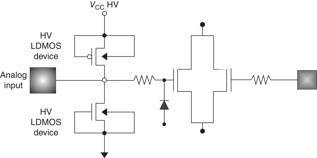
Figure 8.3 Two-stage HV analog input protection using LDMOS transistors, resistor, and diode.
Figure 8.4 shows an example of a two-stage HV analog network that contains an NDMOS element, a series resistor, and a diode element prior to the circuit. In this implementation, the body is grounded. Note that this will require usage of ESD elements whose breakdown voltage to the isolation or substrate is above the application voltage.

Figure 8.4 Two-stage HV analog input protection using GGNMOS LDMOS transistor, resistor, and diode.
Figure 8.5 shows an example of a two-stage HV analog network that contains an NDMOS element, a series resistor, and a diode element with the body floating. This will allow for usage of the LDMOS transistor without isolation breakdown.

Figure 8.5 Two-stage HV analog input protection using floating-body LDMOS transistor.
8.3 Analog ESD Output Circuits
In HV applications, analog ESD solutions for output networks used can be utilized for output drivers.
8.3.1 Analog ESD Output Networks and Distinctions
In HV applications, analog ESD solutions for output networks used for receiver networks can be utilized for output drivers. Some distinctions for output driver networks are as follows:
- Self-protection is an option for large output driver elements.
- Some topologies require ESD networks.
- Isolation voltage conditions must avoid breakdown or limiting the signal swing of the output network.
In HV applications from 5 to 120 V, analog circuitry can be designed to be “self-protecting” without additional ESD networks. For power applications, the physical width of “pull-up” and “pull-down” transistors can be very large. As a result, an ESD network may not be necessary. Self-protecting analog circuits may require specific layout practices that allow for more ESD or EOS robustness than standard LDMOS or DeMOS devices.
In some HV applications, some topologies have only a “pull-down” network and do not allow for a “pull-up” element. An example of this is an “open-drain” topology.
8.3.2 Analog Open-Drain ESD Output Networks
An analog open-drain output network only has a “pull-down” network and does not allow for a “pull-up” element. Figure 8.6 is an example of an HV open-drain network schematic with ESD protection. An HV LDMOS device is electrically connected to the output voltage. The isolation of the LDMOS device is electrically connected to the HV VCC power supply, whereas the body region is electrically connected to ground VSS. An HV LDMOS network is also placed between the open-drain output and the ground. In this element, the isolation is left floating.
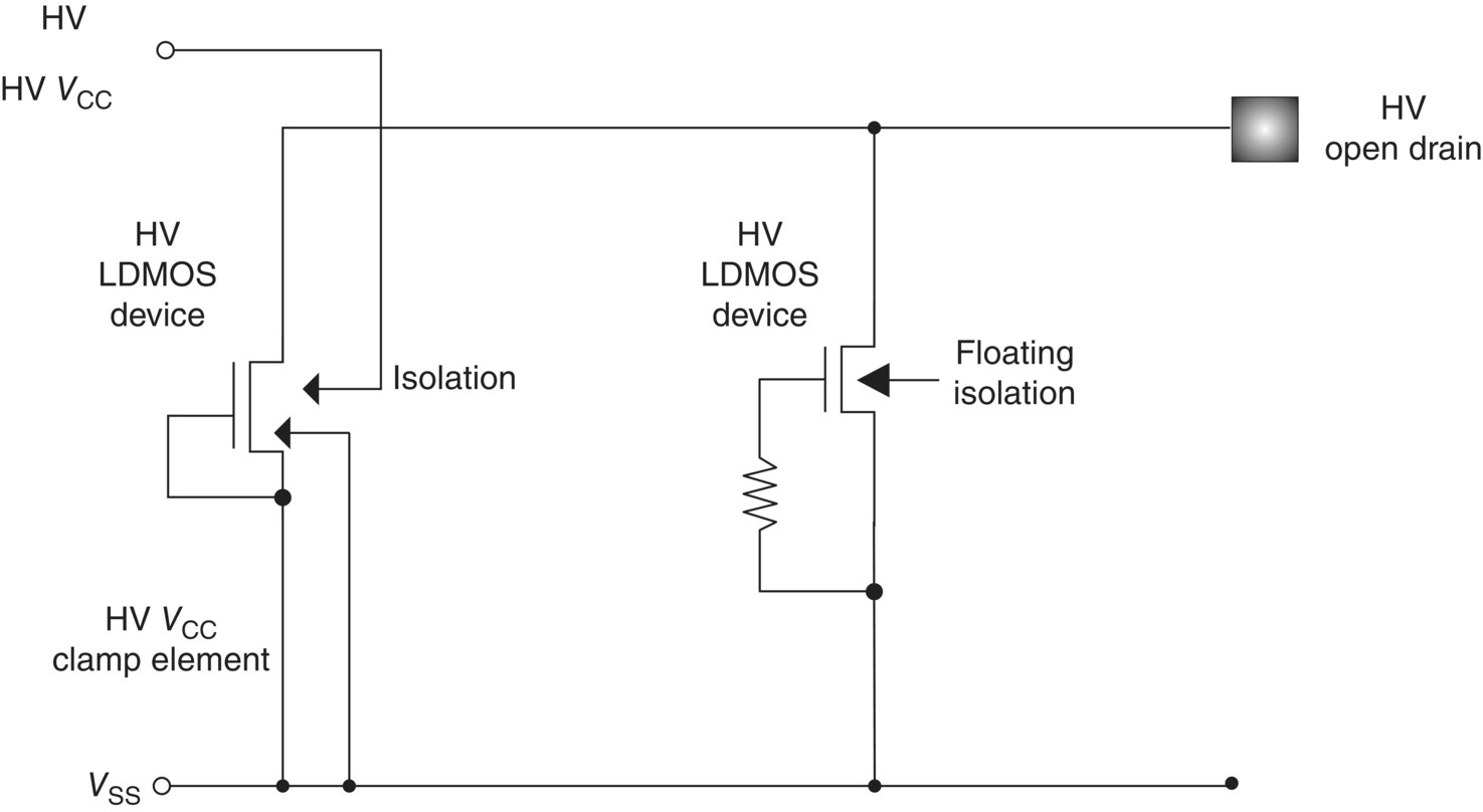
Figure 8.6 HV VCC open-drain output network.
8.4 Analog ESD Ground-to-Ground Networks
In analog and digital-to-analog mixed-signal technology, electrical connectivity and isolation can be established through the ground rails with ESD ground-to-ground networks [15, 16]. These networks can have the following features:
- Unidirectional
- Bidirectional
- Symmetric
- Asymmetric
- Single elements or series (e.g., stack) of elements
In product implementations, the choice of the design is a function of the trade-off of ESD connectivity versus noise isolation. Unidirectionality can prevent current flow or current injection in one direction. Bidirectionality allows flow in both directions between the power rails. Using symmetric versus asymmetric designs allows preferential isolation and capacitive coupling.
8.4.1 Back-to-Back CMOS Diode String
In CMOS technology, LDMOS technology, and BCD technology, ground-to-ground ESD networks can consist of CMOS-based element. CMOS elements can be p+/n-well diodes, gated diodes, or diode-configured MOSFETs. A disadvantage of using an LV CMOS MOSFET is electrical failure of the MOSFET gate structure. Additionally, the devices may need to be electrically isolated for noise and latchup. CMOS diode structures can contain n-wells which collect minority carrier from the substrate.
Using triple well technology, isolation can be achieved to minimize the problem of noise injection by separating from the substrate region. The triple well diode structures will need a power supply voltage electrically connecting to the isolating structures; the issue with this is that the minority carrier will be collected by the analog VDD (AVDD).
8.4.2 HV GGNMOS Diode-Configured Ground-to-Ground Network
In LDMOS technology and BCD technology, ground-to-ground ESD networks can consist of LDMOS-based elements instead of CMOS-based diode elements. Figure 8.7 shows an example of a bidirectional symmetric back-to-back network. One of the advantages of using an LDMOS device is that LDMOS technology is designed for power, whereas CMOS technology is designed for performance.
Figure 8.7 HV ground-to-ground diode-configured LDMOS.
8.5 ESD Power Clamps
ESD power clamps between power supply and ground connections are commonly used in all domains of a semiconductor chip. In this section, HV ESD power clamps will be first discussed, followed by discussion of LV analog and digital domain ESD power clamps [13–18].
8.5.1 ESD Power Clamp Issues for the High-Voltage Domain
In analog design, voltage-triggered networks are commonly used for power applications. In an analog design, there are many power supply requirements. Additionally, the range of power supply voltages is significant. The power supply voltage range can extend from LV CMOS at 1.5 V to UHV levels from 600 to 800 V. As a result, voltage conditions are a more significant issue compared to frequency. In the next section, some HV ESD network and integration are discussed.
8.5.2 HV Domain ESD Protection and ABS MAX
In HV applications, the input power to HV analog sections may be as high as the LDMOS absolute maximum drain voltage rating. As a result, a concern exists of the choice of ESD network to be compliant with the isolation voltages.
8.5.3 HV Domain VIN or VCC Input
Figure 8.8 shows an example where the HV domain has a VIN or VCC input that requires ESD protection. It also shows an example embodiment using a GGNMOS stack network, with a floating body, as well as a GGNMOS return diode element across the power supplies of an amplifier network. The choice of the ESD network will be required to be compliant with the isolation voltages.
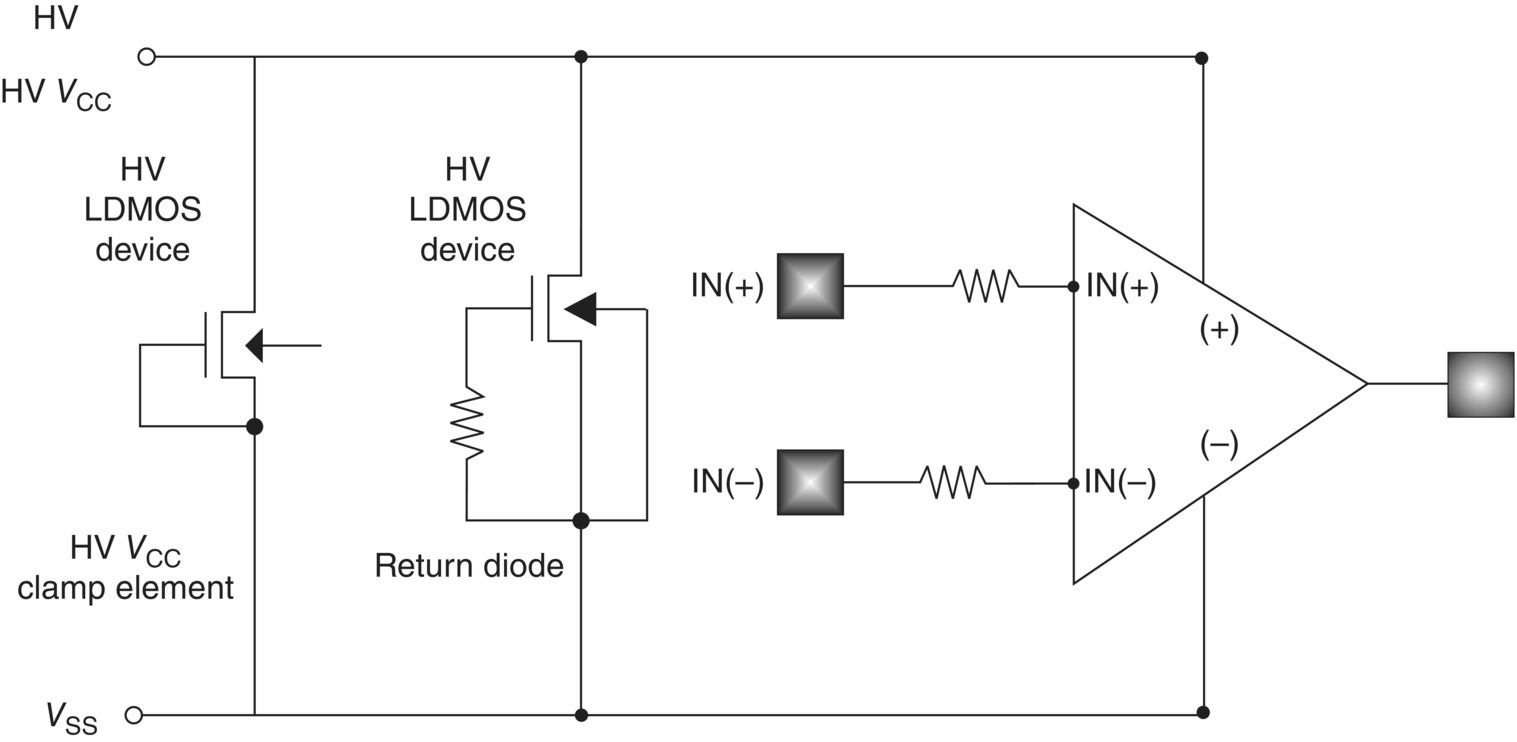
Figure 8.8 HV VCC power input protection scheme.
8.5.4 HV Grounded-Gate NMOS (GGNMOS)
In analog design, a voltage-triggered ESD network commonly used is the HV GGNMOS network [11]. Figure 8.9 is an example of an HV GGNMOS network used for analog and power applications. For analog and power applications, the HV GGNMOS transistor must have a high dielectric breakdown voltage to avoid gate-to-drain breakdown. LDMOS transistors that have breakdown voltage tolerance are commonly used. For power applications, the GGNMOS device utilized must also have an isolation voltage above the application voltage. In many power applications, the “body” can float to avoid electrical breakdown in ESD protection networks.

Figure 8.9 HV ESD GGNMOS.
8.5.5 HV Series Cascode ESD Network
In analog design, a voltage-triggered ESD network commonly used is the HV GGNMOS network. For analog and power applications, the HV GGNMOS transistor must have a high dielectric breakdown voltage to avoid gate-to-drain breakdown. LDMOS transistors that have breakdown voltage tolerance are commonly used. For power applications, the GGNMOS device utilized must also have an isolation voltage above the application voltage. In many power applications, the “body” can float to avoid electrical breakdown in ESD protection networks. Figure 8.10 is an example of an HV GGNMOS network where elements are in a series cascode configuration for HV analog and power applications [11].
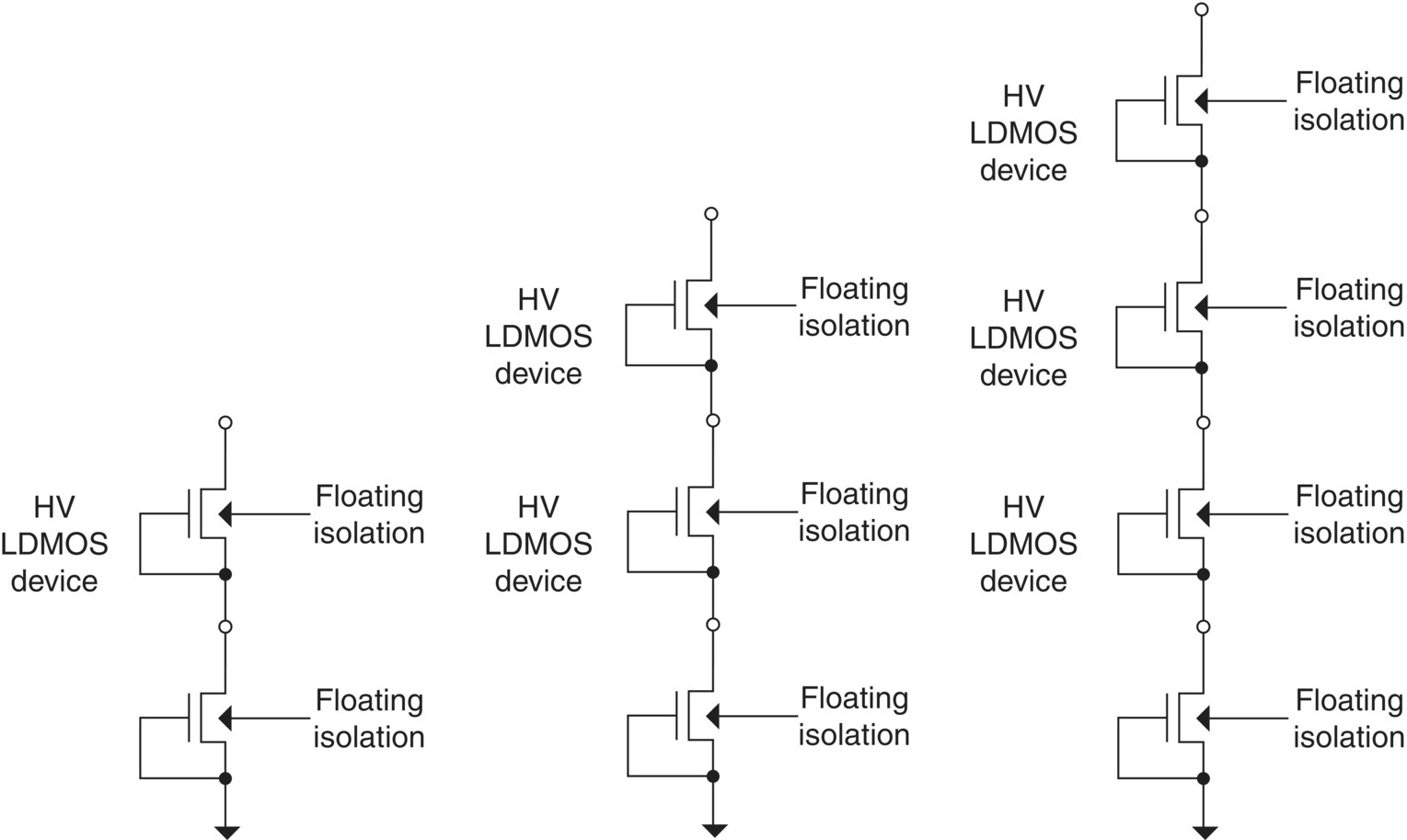
Figure 8.10 HV ESD stacked GGNMOS.
8.5.6 ESD Power Clamp Bidirectionality and Return Diodes
ESD power clamps require bidirectionality to allow current flow in a first direction from VCC to VSS and a second direction from VSS to VCC. Many ESD power clamps are designed to allow current flow from VCC to VSS. As a result, a “return diode” is added to provide current flow in the reverse direction. Figure 8.11 is an example of a “return diode” ESD network that uses an HV GGNMOS. A resistor element is added to the LDMOS gate electrode.
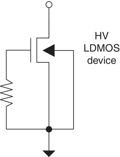
Figure 8.11 HV ESD power clamp return diode.
8.5.7 Alternative Solutions: LDO Current Limits
Alternative solutions exist with the use of voltage and current limiting function internal or external to the circuit function. Current limiting function can be added to the circuit network to control the electrical overcurrent (EOC) issues (Figure 8.12).

Figure 8.12 Alternative LDO current limit.
8.5.8 Alternative Solutions: External EOS Diode
Alternative solutions exist with the use of voltage and current limit external to the circuit function. Some ESD and EOS solutions exist on-chip and some off-chip [12]. Figure 8.13 shows an example of an EOS Schottky diode external to the semiconductor chip.

Figure 8.13 Alternative LDO EOS Schottky diode.
8.6 ESD Power Clamps for Low-Voltage Digital and Analog Domain
For digital applications, ESD power clamp usage began in the mid-1990s and today is a common practice of semiconductor chip design and ESD design synthesis [15–18]. In the later 1990s to early 2000 period, these began to be implemented into analog applications. Development of ESD power clamps and the synthesis into the semiconductor chip architecture are part of the ESD design discipline and an essential component of the art of ESD design. In this section of the chapter, the focus on the classification of the ESD power clamps, key design parameters, the ESD power clamp design window, trigger elements, clamp devices, and issues and problems with ESD power clamp will be discussed.
8.6.1 Classification of ESD Power Clamps
There are many different types of ESD power clamps, but conceptually, they can be classified into different categories. Figure 8.14 shows a diagram of classification of ESD power clamps used for LV analog and digital domains.

Figure 8.14 Classes of ESD power clamps.
ESD power clamps must be tolerant of the power supply voltages observed in the functional semiconductor chip or system of chips. ESD power clamps can be constructed for the native voltage power supply or mixed-voltage power supplies. The ESD power clamps must be tolerant of the semiconductor chips they interface with or the number of power rail voltages contained within a given chip.
Fundamentally, ESD power clamps contain some basic features. The first feature is the transfer of ESD current from one segment of the power grid to a second segment of the power grid. The second feature is the initiation of the ESD power clamp, commonly referred to as a “trigger” state. ESD power clamps can be as simple as one physical device or a complex circuit, or a system. In the simplest case, the trigger feature and the clamp feature can be contained within the same device. In the second classification, the trigger element is independent of the “clamp” feature (e.g., independent trigger element from the clamping feature). There is a critical conceptual concept in the ESD power clamp design synthesis in the separation of the trigger state feature from the clamp feature. The advantage of an independent trigger element is that it provides a second degree of freedom with the separation of the clamping feature from the trigger feature. Whereas a single integrated fashion, there is physical limitation in some devices to achieve both features as desired.
In the third classification, the ESD power clamp is a system of ESD power clamps, with one trigger element for a system of clamp elements, which will be referred to as a “master/slave” architecture. A master/slave system allows integration of a single trigger element but allows distribution of the elements in the chip system.
In the ESD power clamp “trigger feature,” there are many different solutions used for ESD power clamps, but again, they can be simply stated as classifications of trigger elements.
ESD power clamps can have trigger feature that responds to the ESD pulse. The “trigger network” is responsive to a given frequency or transient phenomena. This class of trigger networks will be referred to as “frequency triggering.” Frequency trigger can contain elements that are frequency dependent, such as resistors, capacitors, and inductors [3, 4, 6]. Frequency-triggered networks respond in the frequency domain. ESD trigger elements can also be networks that do not respond in the frequency domain. These ESD trigger networks can also be initiated by overvoltage or overcurrent condition. A class of ESD trigger networks are voltage-triggered elements. Voltage-triggered elements can be initiated in a forward-bias or reverse-bias state of operation.
In this classification, there are additional features that have been added to address other characteristics. Some of these features are as follows:
- Ramping of the power supplies (e.g., power-up or power-down)
- Sequencing of power supplies
- False triggering from system events
- ESD testing precharging phenomena
- ESD testing “trailing pulse” phenomena
8.6.2 ESD Power Clamp: Key Design Parameters
In ESD design synthesis of ESD power clamps, there are key design parameters in the decision of what type of circuit to utilize. The following is a list of key parameters in the ESD design process of ESD power clamps [18]:
- ESD power clamp physical area
- ESD power clamp width
- ESD power clamp current per unit of width metric (A/um)
- ESD power clamp “on-resistance”
- ESD power clamp voltage tolerance
- ESD power clamp latchup robustness
- ESD power clamp false triggering immunity
- ESD power clamp IEC 61000-4-2 responsiveness
- ESD power clamp leakage current
- ESD power clamp capacitance loading
- ESD power clamp frequency response window
- ESD power clamp trigger voltage or current
- ESD return diode
These features and aspects of ESD power clamps will be discussed. These ESD power clamps can be made of diodes, bipolar transistors, MOSFETs, silicon-controlled rectifiers, and LDMOS transistors.
8.6.3 Design Synthesis of ESD Power Clamps
The ESD power clamp “trigger feature” is critical to initiate the ESD power clamp. ESD power clamps can have trigger feature that responds to the ESD pulse through either transient response or voltage levels. The following sections will focus on two major classes of “trigger networks.”
8.6.4 Transient Response Frequency Trigger Element and the ESD Frequency Window
In ESD power clamps, the ESD power clamp trigger element can be a frequency-triggered network or transient response trigger element [18]. Transient response trigger elements are designed to respond to the ESD events. This class of trigger networks will be referred to as “frequency triggering.” Frequency-triggered networks respond in the frequency domain. The frequency trigger can contain elements that are frequency dependent, such as resistors, capacitors, and inductors, in resistor–capacitor (RC), LC, or RLC configurations. In ESD power clamps, the most widely used and most popular is the RC network. The RC-triggered network is also known as “RC discriminator” network, due to it providing frequency selection in the ESD power clamp frequency domain [14, 15]. By providing a separate RC filter network, the frequency response of the trigger network will not be dependent on the inherent native frequency response of a semiconductor device and can be “tuned” to the desired frequency. In the majority of applications, the RC discriminator network is tuned to be responsive to the human body model (HBM) and machine model (MM) pulse events. One of the key advantages of frequency-triggered ESD clamps is that it is a function of the transient or rising edge, not the voltage level of the power grid.
In the frequency-triggered network, the resistor and capacitor elements can be passive or active semiconductor elements. The choice of what element to use is a function of the technology, area utilization, voltage tolerance, and device responsiveness. The resistor used for the RC network can be the following:
- Polysilicon resistor element
- Diffused resistor element
- “On” n-channel transistor element
- “On” p-channel transistor element
The capacitor element typically used for the RC network is as follows:
- MOS capacitor
- MIM capacitor
8.6.5 ESD Power Clamp Frequency Design Window
Figure 8.15 shows the ESD power clamp frequency window [18]. It provides a frequency plot highlighting the typical frequency of ESD events, overlaying the typical design point for ESD power clamps. Typically, ESD power clamps are designed to respond to the HBM and MM events (Figure 8.16). ESD power clamps are not designed to respond to charged device model (CDM) events. In addition, the ESD power clamps are not to be initiated by the power-up and power-down of the semiconductor chip or system. The ESD power clamps are not to be initiated by system events, leading to “false triggering.”

Figure 8.15 ESD power clamp frequency window.
As a result, there is a defined frequency window that is acceptable for ESD power clamps and the frequency range of these networks.

Figure 8.16 Example of frequency-triggered ESD power clamp for analog applications highlighting the trigger network.
8.6.6 Design Synthesis of ESD Power Clamp: Voltage-Triggered ESD Trigger Elements
In ESD power clamps, the ESD power clamp trigger element can be a current- or voltage- triggered ESD network [13–18]. Voltage-triggered elements are designed to respond to the ESD events when the voltage exceeds the trigger condition. These ESD power clamps will turn on when the voltage exceeds the trigger state. As a result, it is not dependent on the frequency of the transient event. As a result, this turns “on” the circuitry independent if it is an ESD event, EOS event, or any overvoltage or overcurrent state. These ESD power clamps are not to be initiated by the power-up and power-down of the semiconductor chip or system except when they are in an overvoltage state.
ESD voltage-triggered elements can be either forward-bias or reverse-bias elements or circuits [18]. For reverse-bias trigger networks, the following are typically utilized:
- Zener breakdown diode
- Polysilicon diode
- CMOS LOCOS-defined metallurgical junction diode
- CMOS shallow trench isolation (STI)-defined metallurgical junction diode
- Bipolar transistor collector-to-substrate junction diode
- Bipolar transistor base–collector junction diode
- Bipolar transistor emitter–base junction diode
- Bipolar transistor collector-to-emitter configuration
For forward-bias trigger networks, typically, a “diode string” or series cascode configured diodes are used to establish the trigger voltage. For forward-bias trigger networks, the following are typically utilized [18]:
- CMOS LOCOS-defined metallurgical junction diode
- CMOS STI-defined metallurgical junction diode
- Bipolar varactor (forward-bias configuration)
- Bipolar transistor base–collector junction diode
- Bipolar transistor base–emitter junction diode
In some applications, to achieve the desired trigger voltage, the forward-bias elements can be combined with reverse-bias elements. By using the forward-bias trigger elements in series with the reverse-bias trigger element, higher trigger voltage states are achieved (Figure 8.17).
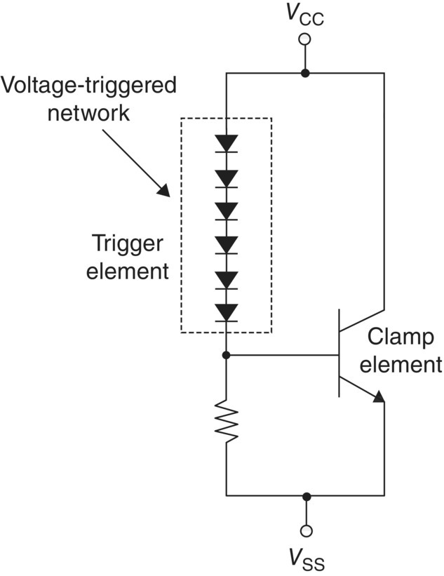
Figure 8.17 Example of voltage-triggered ESD power clamp highlighting the trigger network.
8.6.7 Design Synthesis of ESD Power Clamp: The ESD Power Clamp Shunting Element
For ESD protection power clamps, the two basic functions are the trigger network and the “shunt” network (e.g., also referred to as “clamp element”) [18]. The role of the shunt element is to provide a current path in the alternative current loop to discharge the ESD current. For the effectiveness of the ESD power clamp, there are a few desired features of the ESD clamp element:
- Low impedance: Provide a low impedance path (e.g., a low “on-resistance”)
- ESD robustness: Provide an ESD robust solution (e.g., discharge the ESD current without failure below the desired ESD specification)
- Scalable: Scalable element with physical size (e.g., width, length, perimeter, or area)
There are some additional desired characteristics of the ESD power clamp “shunt element.” These consist of the following:
- ESD power clamp trigger condition versus ESD power clamp shunt failure
- ESD clamp element ESD robustness width scaling
- ESD on-resistance
8.6.8 ESD Power Clamp Trigger Condition versus Shunt Failure
For proper operation of the ESD power clamp, the trigger network will require to initiate prior to the overvoltage or overcurrent of the ESD “shunt” clamp element [18]. In the frequency domain, if the ESD network trigger does not respond to a specific ESD event, the trigger network will not respond effectively, and the ESD “shunt clamp” will discharge according to its native breakdown event. For a MOSFET “shunt” element, the element will undergo MOSFET drain-to-source snapback. For a bipolar transistor, the bipolar element will undergo collector-to-emitter breakdown.
8.6.9 ESD Clamp Element: Width Scaling
It is desirable to have the ESD results scale with the ESD clamp “shunt” element size. The ESD robustness will scale with the physical width given the following conditions:
- Frequency tuning: Proper frequency “tuning” of the trigger network (e.g., responsive to the ESD event) for MOSFET gate-driven networks or bipolar base-driven networks
- Drive circuit: Adequate current drive and current-drive distribution for bipolar base-driven networks
- Layout symmetry: Layout optimization of clamp element
- Ballasting: MOSFET drain ballast (or bipolar emitter ballast) adequate to provide uniformity
- Power bus connectivity: Electrical connection to power bus and ground rail well distributed in the ESD power clamp “clamp element” region of the circuit
8.6.10 ESD Clamp Element: On-Resistance
It is desirable to have the ESD clamp on-resistance which reduces with the size of the MOSFET or bipolar clamp element. The lower the ESD clamp on-resistance, the lower the total resistance through the alternative current loop. The lower the resistance in the ESD current loop, the lower the node voltage at the bond pad node. As the impedance of the power bus and the ESD clamp element is reduced, the allowed resistance for the ESD signal pin network can be higher and achieve the same signal pin ESD robustness. Hence, lowering the ESD power clamp resistance allows for a smaller ESD network at the signal pin (e.g., smaller network with lower capacitance).
The ESD clamp on-resistance will scale down with the clamp element device size, given that the element does not undergo current saturation effects, self-heating, or poor current distribution. Hence, if the ESD power clamp element is large enough and self-heating is kept to a minimum, the “on-resistance” will scale with the width scaling.
8.6.11 ESD Clamp Element: Safe Operating Area
The ESD “clamp element” must remain in the safe operating area (SOA) of the device to avoid failure of the ESD power clamp network. To avoid electrical failure of the ESD clamp element prior to the achieve ESD objective, the clamp element of the ESD power clamp must remain below a voltage absolute maximum (VABS MAX) and a current absolute maximum (IABS MAX) of the clamp element.
8.7 ESD Power Clamp Issues
ESD power clamps have some unique issues as a result of being placed within the power grid of a semiconductor chip. The issues will be briefly discussed, followed by examples in the future sections on how to address these issues.
8.7.1 Power-Up and Power-Down
ESD power clamps are to remain in an “off-state” when a semiconductor chip is in a power-up state, a power-down state, and a quiescent powered state [18]. The different solutions to avoid initiation of the power clamps during power-up and power-down ramping are as follows:
- Frequency window: Trigger networks do not respond to these frequencies.
- Feedback networks: Feedback networks are placed to avoid response to power up.
- Enable/disable functions: Logic can be integrated into the trigger network to “enable” or “disable” the ESD power clamp as desired.
8.7.2 False Triggering
ESD power clamps can be “false triggered” as a result of pulse events from signals, overcurrent, overvoltage, or “spikes” during test, burn-in, or other reliability stresses. The different solutions to avoid initiation of the power clamps during power-up and power-down are as follows:
- Overcurrent protection: Overcurrent protection can be integrated to avoid the ESD power clamp outside of its SOA.
- Frequency window: Trigger networks do not respond to these frequencies of “spikes.”
- Feedback networks: Feedback networks are placed with hysteresis.
- Enable/disable functions: Logic can be integrated into the trigger network to “enable” or “disable” the ESD power clamp as desired.
8.7.3 Precharging
Precharging events can occur during ESD testing that can influence the ESD power clamp networks [18]. In the process of ESD testing, poor isolation of the test source from the device under test (DUT) can lead to a precharging phenomenon in the semiconductor chip. After an ESD pulse is applied, a low-level current bleeds from the HV source to the DUT without proper “switch” isolation. The solutions for the “precharging” solution are as follows:
- ESD power clamp precharge “bleed” device: A high impedance element can be placed in parallel to the ESD power clamp to allow the bleeding of charge from the VDD to the VSS power rail. The “bleed device” can be a resistor. This can be placed local to the device or nonlocal to the ESD power clamp.
- ESD test system modification: Modification of the ESD stress test system by providing proper isolation.
8.7.4 Postcharging
A postcharging event from ESD simulators is also present that can influence the ESD test results [18]. After the ESD event occurs, a low-level current “tail” exists in the simulators that continues to charge the signal pins or power pins. In the process of ESD testing, poor isolation of the test source from the DUT can lead to a postcharging phenomenon in the semiconductor chip. As in the precharging event, the postcharging events can lead to an anomalous ESD test result.
8.8 ESD Power Clamp Design
In this section, examples of different circuit topologies will be shown to highlight some of previously discussed issues. Native power supply voltage and nonnative ESD power clamps will be discussed.
8.8.1 Native Power Supply RC-Triggered MOSFET ESD Power Clamp
Figure 8.18 shows an example of the most commonly used ESD power clamp in the semiconductor industry, the RC-triggered MOSFET ESD power clamp. The RC discriminator network discriminates between ESD events and spurious events or power-up and power-down if properly tuned. The RC trigger typically is “tuned” to respond to the ESD HBM and MM pulse events.

Figure 8.18 RC-triggered MOSFET ESD power clamp.
The inverter stages serve two purposes. Firstly, it allows for the tuning of the RC network without the loading of the first inverter gate capacitance influencing the RC “tuning.” Secondly, it serves a drive stage for “driving” the ESD clamp element. In recent years, to improve the responsiveness, the three inverter stages have been reduced to a single stage. The advantage of this is to improve the responsiveness. The disadvantage of the single inverter is the increase in the size of the single inverter stage and the lack of isolation between the RC discriminator tuning and the load of the inverter stage and output network. This network is also suitable for native voltage conditions. Given higher-voltage power domains, all elements in the circuitry must be voltage tolerant to that given power domain.
8.8.2 Nonnative Power Supply RC-Triggered MOSFET ESD Power Clamp
In many mixed-voltage or mixed-signal applications, different power clamps are required based on the voltage of the power domain. Figure 8.19 shows an RC-triggered MOSFET power clamp, where the second MOSFET is used to lower the voltage across all the elements in the lower element. In the design synthesis of this network, the “drop-down” device lowers the voltage across all elements in the ESD power clamp. Hence, it provides two roles: (1) serves as a “level shift” of the voltage level and (2) converts the power bus of the ESD network into a “dummy ESD power rail bus” instead of the actual power rail bus. In this case, a MOSFET is used for the “level” shifting network. Alternative ESD “level” shift elements utilized can include diode string elements.

Figure 8.19 Series cascode RC-triggered MOSFET ESD power clamp.
8.8.3 ESD Power Clamp Networks with Improved Inverter Stage Feedback
To provide better control of the ESD clamp element and avoid false triggering, the “latching characteristics” of the inverter drive stage can apply well-known feedback methods. Well-known feedback techniques in CMOS logic include “half-latch” or “full-latch” circuit concepts. Figure 8.20 shows an example of an ESD power clamp with a CMOS half-latch PMOS keeper element. This provides improved control of the MOSFET output gate, which can improve intolerance to false triggering or avoid low-level leakage of the output MOSFET.

Figure 8.20 CMOS RC-triggered clamp with CMOS PFET half-latch keeper feedback.
The second method to improve the “latching characteristics” of the inverter drive stage can apply well-known “full-latch” circuit concepts. Figure 8.21 shows an example of an ESD power clamp with a CMOS full-latch feedback network [18]. The integration of the full inverter for the feedback forms a “SRAM-like” latch between the ESD power clamp last inverter and the feedback inverter. As with the “half-latch” feedback, this provides improved control of the MOSFET output gate, which can improve intolerance to false triggering or avoid low-level leakage of the output MOSFET.

Figure 8.21 CMOS RC-triggered clamp with CMOS PFET full-latch keeper feedback.
Other techniques for improving the control of the ESD power clamp from false triggering can be applied. As the feedback is brought to the earlier stages, the size of the feedback elements can be reduced. The third method is placement of a PMOS device above the inverters. Figure 8.22 shows an example of an ESD power clamp with a PMOS element within the logic [18].

Figure 8.22 CMOS RC-triggered clamp with CMOS PFET cascade feedback.
8.8.4 Forward-Bias Triggered ESD Power Clamps
In some applications, the presence of a frequency-triggered network is undesirable. RC-triggered ESD MOSFET networks provide ESD protection for frequency dependent applications [18]. For example, given the frequency response of the system, such as a cell phone, is predefined, it may be not be advisable to place another frequency-dependent circuit in a small system (e.g., altering the frequency response of the poles and zeros in the frequency domain). As a result, some circuit design teams desire voltage-triggered networks for RF CMOS instead of frequency-triggered networks. Figure 8.23 is an example of a forward-bias voltage-triggered ESD MOSFET network. The advantage of this network is that it responds to all overvoltage events or overcurrent conditions. The number of diodes is chosen to turn on prior to the MOSFET snapback voltage of the ESD clamp element. This network has a wide frequency window and is not sensitive to power-up, power-down, or false triggering events and does provide overcurrent and overvoltage protection.
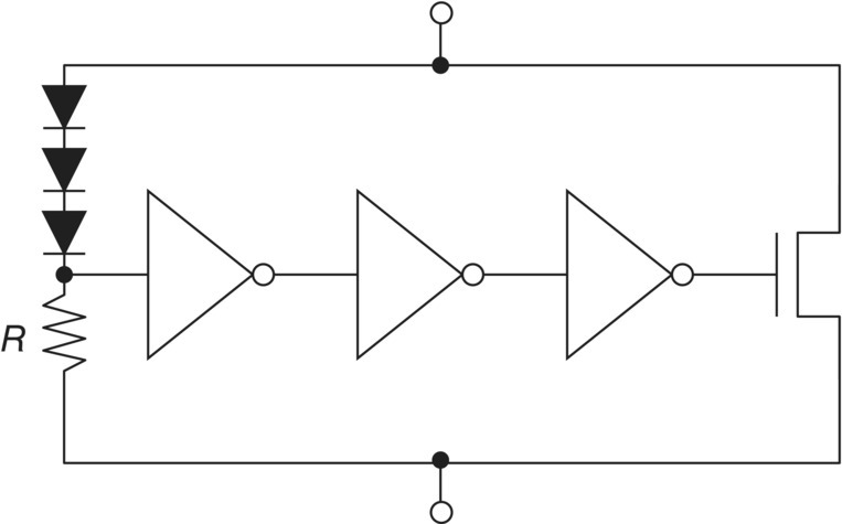
Figure 8.23 Forward-bias voltage-triggered ESD power clamps.
8.8.5 IEC 61000-4-2 Responsive ESD Power Clamps
For applications that are required to respond to the IEC 61000-4-2 pulse event, not all circuit topologies are suitable. For the IEC 61000-4-2 event, there is a fast current pulse which is of considerable magnitude. Hence, to address the frequency response and current magnitude, many ESD power clamps are required to be modified.
During the IEC 61000-4-2 event on the chassis or ground line of a system, a negative pulse occurs on the VSS power rail or substrate. This can initiate the RC-triggered network from the negative pulse event. But the elements in the RC discriminator must be responsive, or circuit failure can occur. The resistor and capacitor element choices must be responsive. Resistors, such as polysilicon resistors, may be slow to respond to fast events.
Figure 8.24 is an example of an IEC 61000-4-2 event responsive ESD MOSFET network. The advantage of this network is that the p-channel MOSFET is more responsive than a polysilicon resistor element. Additionally, so that the inverter drive network is more responsive, only a single inverter stage is implemented.

Figure 8.24 IEC 61000-4-2 responsive ESD power clamp.
8.8.6 Precharging and Postcharging Insensitive ESD Power Clamps
ESD test systems or residual charge can influence the “state” of an RC-triggered MOSFET clamp before or after ESD stress. With charge on the VDD power rail, the voltage state of the RC-triggered MOSFET can be precharged and close the MOSFET snapback voltage of the ESD clamp device. On the first discovery of this issue, it was noted by R. Ashton that products, with RC-triggered power clamps, that were inherently “leaky” had better ESD results than products whose VDD leakage was low. It was from this discovery that Ashton discovered the issue of ESD test system leading to residual charge on the power grid of the semiconductor chip, influencing the prestate of the ESD power clamp. It was noted that the charge on VDD power rail leads to the MOSFET snapback of the output device prior to initiation of the RC discriminator response.
Figure 8.25 is an example of an ESD power clamp network with a “bleed” element to provide discharging of the ESD precharging event or a postcharging event. Placing a high impedance element that bleeds the charge off of the power rail can avoid the ESD test system-induced operation failure of the ESD power clamp element.

Figure 8.25 Precharging and postcharging insensitive ESD power clamp.
8.8.7 ESD Power Clamp Design Synthesis and Return Diode
ESD power clamps require bidirectionality to allow current flow in a first direction from analog or digital VDD to VSS and a second direction from VSS to analog or digital VDD. As a result, a “return diode” is added to provide current flow in the reverse direction. Figure 8.26 is an example of a “return diode” ESD network that uses an LV CMOS diode in parallel with an RC-triggered ESD power clamp.
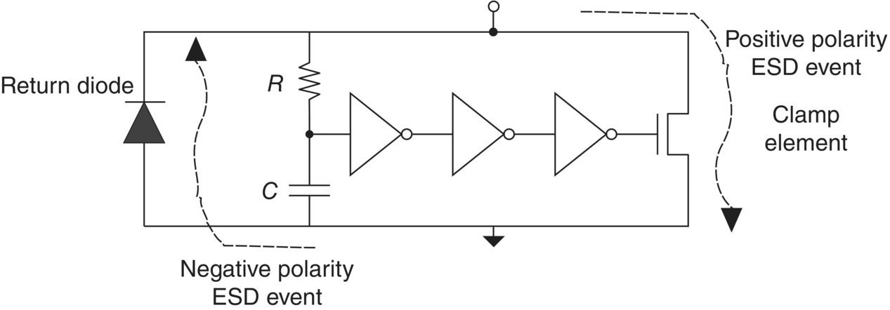
Figure 8.26 Analog ESD power clamp and return diode.
8.9 Bipolar ESD Power Clamps
Bipolar and bipolar-CMOS (BiCMOS) technologies are used today for analog and mixed-signal semiconductor chips. In a mixed-signal semiconductor chip that utilizes bipolar transistors, analog and digital domains are separated. Bipolar transistors typically have a higher power supply voltage. Additionally, in many bipolar applications, a negative power supply voltage is also used. For these bipolar power domains, bipolar power clamps are used [16].
8.9.1 Bipolar ESD Power Clamps with Zener Breakdown Trigger Element
Figure 8.27 is an example of a bipolar ESD power clamp [16]. In this ESD bipolar power clamp, a single transistor is placed between the two power supplies in a collector-to-emitter configuration. The transistor is to be used to discharge the ESD current from the VCC power rail to the VSS ground rail. The trigger element is a Zener diode which undergoes electrical breakdown. When the voltage across the trigger element reaches the breakdown voltage of the Zener diode, the current flows through the Zener diode and into the base of the bipolar transistor. This base-driven network responds to overvoltage conditions in the semiconductor chip. Since it is a voltage-triggered network, it has a wide frequency window of operation; the frequency response is limited to the frequency response of the Zener diode and its bipolar transistor.

Figure 8.27 Reverse breakdown Zener-triggered bipolar ESD power clamps.
8.9.2 Bipolar ESD Power Clamps with Bipolar Transistor BVCEO Breakdown Trigger Element
Figure 8.28 is an example of a BVCEO voltage-triggered bipolar ESD power clamp. In this ESD bipolar power clamp, a single transistor is placed between the two power supplies in a collector-to-emitter configuration [16]. A second transistor is used as the trigger element and is also placed in a common-emitter (C-E) configuration. The clamp transistor element is a high-breakdown (HB) transistor and is to be used to discharge the ESD current from the VCC power rail to the VSS ground rail. The trigger element is a low breakdown (LB) voltage (e.g., BVCEO) npn transistor which undergoes electrical breakdown. When the voltage across the trigger element reaches the BVCEO breakdown voltage, the current flows through the trigger element and into the base of the bipolar transistor. This base-driven network responds to overvoltage conditions in the semiconductor chip. Since it is a voltage-triggered network, it has a wide frequency window of operation; the frequency response is limited to the frequency response of the two transistors.
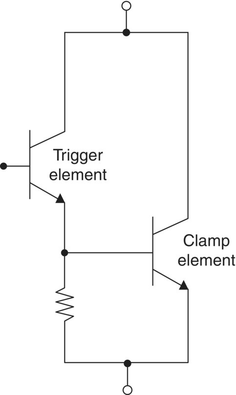
Figure 8.28 Bipolar ESD power clamps with BVCEO breakdown trigger element.
8.10 Closing Comments and Summary
This chapter focused on analog and ESD integration. It also discussed analog signal pin input circuitry to ESD power clamps. A more in-depth look at ESD power clamp issues and solutions was shown.
Chapter 9 discusses system-level issues associated with EOS in chips, printed circuit boards (PCBs), and systems. EOS protection device classifications, symbols, and types for both overvoltage and overcurrent conditions will be highlighted. System-level and system-like testing methods, such as IEC 61000-4-2 and IEC 61000-4-5, and human metal model (HMM) waveforms and methods will be reviewed. Examples of PCB design for digital-to-analog systems will also be provided.
References
- 1. A.B. Glasser and G.E. Subak-Sharpe. Integrated Circuit Engineering. Reading, MA: Addison-Wesley, 1977.
- 2. A. Grebene. Bipolar and MOS Analog Integrated Circuits. New York: John Wiley & Sons, Inc., 1984.
- 3. D.J. Hamilton and W.G. Howard. Basic Integrated Circuit Engineering. New York: McGraw-Hill, 1975.
- 4. A. Alvarez. BiCMOS Technology and Applications. Norwell, MA: Kluwer Academic Publishers, 1989.
- 5. R.S. Soin, F. Maloberti, and J. Franca. Analogue-Digital ASICs, Circuit Techniques, Design Tools, and Applications. Stevenage, UK: Peter Peregrinus, 1991.
- 6. P.R. Gray and R.G. Meyer. Analysis and Design of Analog Integrated Circuits. 3rd Edition. New York: John Wiley & Sons, Inc., 1993.
- 7. F. Maloberti. Layout of analog and mixed analog-digital circuits. In: J. Franca and Y. Tsividis (Eds). Design of Analog-Digital VLSI Circuits for Telecommunication and Signal Processing. Upper Saddle River, NJ: Prentice Hall, 1994.
- 8. D.A. Johns and K. Martin. Analog Integrated Circuit Design. New York: John Wiley & Sons, Inc., 1997.
- 9. R. Geiger, P. Allen, and N. Strader. VLSI: Design Techniques for Analog and Digital Circuits. New York: McGraw-Hill, 1990.
- 10. A. Hastings. The Art of Analog Layout. Upper Saddle River, NJ: Prentice Hall, 2006.
- 11. V. Vashchenko and A. Shibkov. ESD Design for Analog Circuits. New York: Springer, 2010.
- 12. S. Voldman. Electrical Overstress (EOS): Devices, Circuits, and Systems. Chichester, UK: John Wiley & Sons, Ltd, 2013.
- 13. S. Voldman. ESD Basics: From Semiconductor Manufacturing to Product Use. Chichester, UK: John Wiley & Sons, Ltd, 2012.
- 14. S. Voldman. ESD: Physics and Devices. Chichester, UK: John Wiley & Sons, Ltd, 2004.
- 15. S. Voldman. ESD: Circuits and Devices. Chichester, UK: John Wiley & Sons, Ltd, 2005.
- 16. S. Voldman. ESD: RF Circuits and Technology. Chichester, UK: John Wiley & Sons, Ltd, 2006.
- 17. S. Voldman. ESD: Failure Mechanisms and Models. Chichester, UK: John Wiley & Sons, Ltd, 2009.
- 18. S. Voldman. ESD: Design and Synthesis. Chichester, UK: John Wiley & Sons, Ltd, 2011.