
10
Latchup Issues for Analog Design
10.1 Latchup in Analog Applications
CMOS latchup is a concern in advanced semiconductor CMOS, BiCMOS, and bipolar–CMOS–LDMOS (BCD) technologies within a given circuit, between adjacent circuits, and between domains [1–59]. Due to technology scaling, the physical distances between p-channel MOSFETs and n-channel MOSFETs continue to be reduced in the periphery and core of circuits. With density scaling, the number of I/O circuits increases according to Rent’s rule. As a result, the aspect ratio of peripheral I/O circuitry continues to move toward “long/narrow I/O standard cells” with decreased spacing between adjacent I/O standard cells. Hence, the interaction between adjacent I/O (e.g., I/O to I/O) will continue to be a design issue associated with CMOS latchup. In addition, with mixed signal (MS) and system on chip (SOC), the placement of circuits of different domains can also lead to CMOS latchup concerns.
Figure 10.1 shows possible latchup issues in a semiconductor chip. The focus in this chapter will be on the issue of I/O-to-I/O latchup [6, 7], guard rings [8–18], through-silicon via (TSV) [32–39], deep trench [40–46], and active guard rings [47–59]. Test structures that address I/O-to-I/O interactions will be discussed. Electrical measurements of parasitic bipolar current gain and analysis will be shown.

Figure 10.1 Latchup.
10.2 I/O-to-I/O Latchup
I/O-to-I/O latchup can occur with the formation of a lateral parasitic pnpn network between two adjacent I/O cells [6]. With two adjacent I/O standard cells, latchup can occur in multiple interactions due to the two PFETs and two NFETs. The adjacent standard cells can be the following:
- Digital-to-analog I/O
- Analog I/O to analog I/O
- High-voltage I/O to analog I/O
- Analog I/O to ESD
- Analog I/O to ESD power clamp
- Analog I/O to grounded n-well plate
- Analog I/O to decoupling capacitor
I/O-to-I/O latchup can occur between two n-well regions of adjacent analog standard cell and an adjacent structure. To quantify I/O-to-I/O latchup concerns, a structure can be formed to address all interactions. Two four-stripe structures can be formed in a test structure as shown in Figure 10.2.
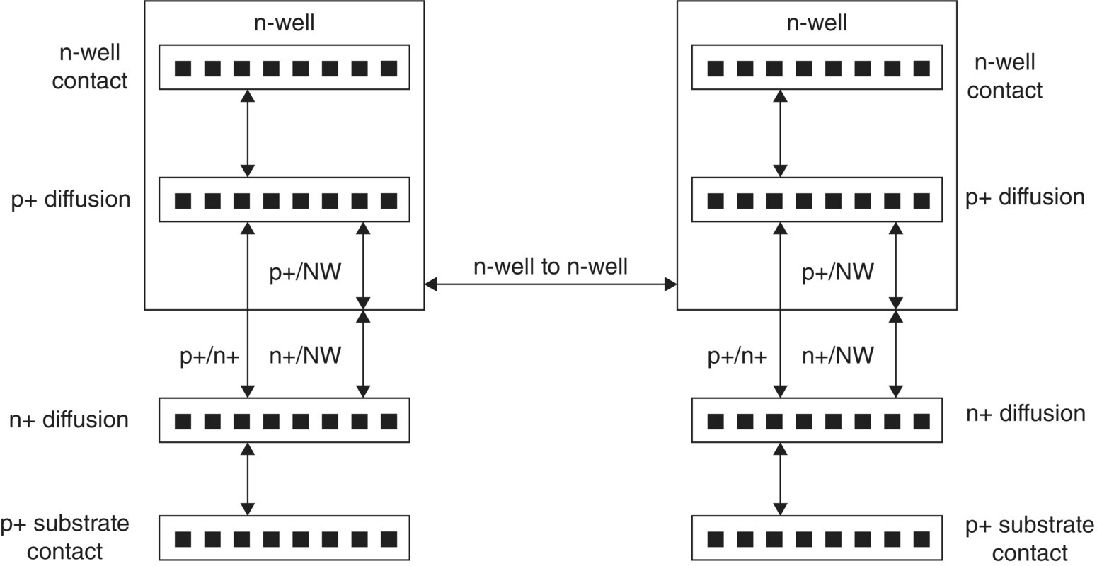
Figure 10.2 Standard cell I/O-to-I/O latchup test structure.
10.3 I/O-to-I/O Latchup: N-Well to N-Well
I/O-to-I/O latchup can occur between two n-well regions of adjacent analog standard cells. A lateral pnpn can be formed between the first I/O network PFET, its own n-well, the p-substrate, and an adjacent n-well (Figure 10.3) [6].
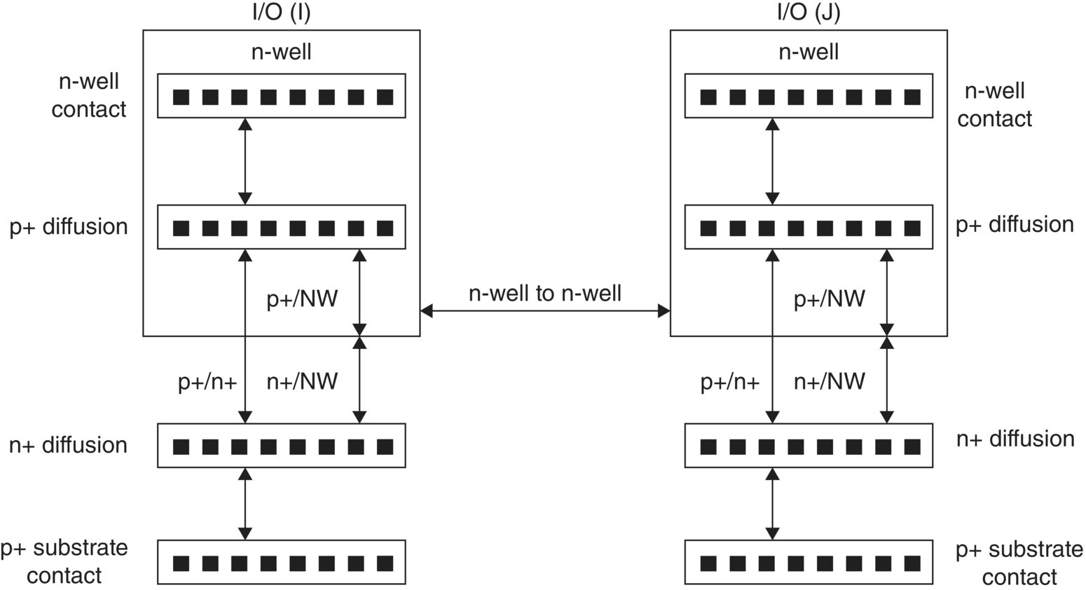
Figure 10.3 Standard cell I/O to I/O highlighting the n-well-to-n-well spacing.
The critical parameter of interest is the spacing between the two adjacent cells forming a lateral npn between the first and second n-well regions. As the technologies are scaled, the bond pad will be scaled, decreasing the space between the two adjacent n-well regions. As the spacing decreases, the npn bipolar current gain will increase with the n-well-to-n-well space. Note that this interaction is symmetrical and bidirectional (e.g., there are two pnpn parasitic elements formed). Tables 10.1 and 10.2 show the lateral bipolar npn gain as a function of n-well-to-n-well spacing at 25 and 125°C, respectively (Figures 10.4 and 10.5).
Table 10.1 Lateral NW–NW bipolar current gain (25°C)
| Structure | Well to well (µm) | NW–NW npn beta |
| I/O to I/O | 5 | 0.6 |
| I/O to I/O | 10 | 0.5 |
| I/O to I/O | 15 | 0.3 |
| I/O to I/O | 20 | 0.2 |
Table 10.2 Lateral NW–NW bipolar current gain (125°C)
| Structure | Well to well (µm) | NW–NW npn beta |
| I/O to I/O | 5 | 1.8 |
| I/O to I/O | 10 | 1.6 |
| I/O to I/O | 15 | 1.45 |
| I/O to I/O | 20 | 1.3 |

Figure 10.4 Standard cell I/O to I/O highlighting the bipolar current gain as a function of the n-well-to-n-well spacing (25°C).

Figure 10.5 Standard cell I/O to I/O highlighting the bipolar current gain as a function of the n-well-to-n-well spacing (125°C).
10.4 I/O-to-I/O Latchup: N-Well to NFET
A lateral pnpn can be also formed between the first I/O network PFET, its own n-well, the p-substrate, and the adjacent n-channel MOSFET device of the second I/O cell (Figure 10.6) [6]. In this case, the NFET pull-down source serves as the emitter of the pnpn network. Test structures varied all the design variables to evaluate the npn bipolar current gain between the n-well of the first standard cell and the adjacent “NFET” structure.

Figure 10.6 Standard cell I/O to I/O highlighting the n-well to n+ spacing.
Table 10.3 contains experimental results of NW to n+ where the well-to-well spacing was varied from 15 to 5 µm (Figures 10.7 and 10.8). Table 10.3 is data for a p+/n+ spacing of 2.4 µm.
Table 10.3 Lateral NW–n+ bipolar current gain as a function of well to well (25°C)
| Structure | Well to well (µm) | NW–n+ npn beta |
| I/O to I/O | 5 | 0.5 |
| I/O to I/O | 10 | 0.39 |
| I/O to I/O | 15 | 0.3 |
An interesting experimental results showed that as the NFET (I/O = 2) became closer to the n-well (I/O = 2), the bipolar current gain between the n-well (I/O = 1) and NFET (I/O = 2) decreased!.

Figure 10.7 Standard cell I/O to I/O highlighting the bipolar current gain as a function of the n-well to adjacent n+ spacing (25°C).

Figure 10.8 Standard cell I/O to I/O highlighting the bipolar current gain as a function of the n-well to adjacent n+ spacing (125°C).
Table 10.4 shows the bipolar gain of NW(1) –to – n+ (2), as the p+/n+ spacing is reduced in the design. The lateral bipolar current gain decreases from 0.5 to 0.4 (at 25°C); note that it decreased instead of increasing. This is counterintuitive. The reason for the reduction is the NW(2) starts to collect the carrier from NW(I/O = 1) to n + (I/O = 2), serving as a “pseudo guard ring” for this interaction [6].
Table 10.4 Lateral NW–n+ bipolar current gain (25°C) versus p+/n+ space
| p+/n+ (µm) | Well to well (µm) | NW–n+ npn beta |
| 2.4 | 5 | 0.5 |
| 1.2 | 5 | 0.44 |
| 0.8 | 5 | 0.4 |
10.5 I/O-to-I/O Latchup: NFET to NFET
A third interaction of interest is the lateral npn bipolar transistor formed between the two adjacent NFET devices [6]. In this case, only a lateral npn is formed (Figure 10.9). Table 10.5 shows the experimental results as a function of the n-well-to-n-well spacing (leading to a smaller base width between the two NFETs).

Figure 10.9 Standard cell I/O-to-I/O structure highlighting the n+ to adjacent n+ spacing.
Table 10.5 Lateral NFET–NFET current gain (125°C)
| Structure | Well to well (µm) | n+ to n+ npn beta |
| I/O to I/O | 5 | 0.28 |
| I/O to I/O | 10 | 0.22 |
| I/O to I/O | 15 | 0.20 |
| I/O to I/O | 20 | 1.3 |
10.6 I/O-to-I/O Latchup: N-Well Guard Ring between Adjacent Cells
In some foundries, an n-well guard ring is placed between the two adjacent cells. With the placement of the n-well guard ring, carriers will be collected by the adjacent n-well guard ring instead of the adjacent I/O cell’s n-well or NFET region [6]. Figure 10.10 shows the standard cell with an n-well guard ring diffusion, and Table 10.6 shows the experimental results. In this implementation, the issue is the npn bipolar current gain between the PFET tub and the n-well guard ring, as well as the n-well guard ring series resistance.

Figure 10.10 Standard cell I/O to I/O highlighting the n-well guard ring separating the two adjacent I/O circuits.
Table 10.6 Lateral NW-to-NW guard ring current gain (25°C)
| Structure | Well-to-guard ring (µm) | n+ to n guard ring npn beta |
| I/O to I/O | 5 | 6.0 |
| I/O to I/O | 10 | 5.0 |
| I/O to I/O | 15 | 4.0 |
| I/O to I/O | 20 | 3.4 |
10.7 Latchup of Analog I/O to Adjacent Structures
Many CMOS latchup problems today occur due to the placement of circuits adjacent to each other without verification of the interaction. This will become more important in analog design as technology spacings are reduced in CMOS, BiCMOS, BCD, and high-voltage and ultrahigh-voltage technologies.
10.7.1 Latchup in Core-Dominated Semiconductor Chips
Many CMOS latchup problems in analog design occur due to low pin count in a chip periphery where extra space exists. In these low pin count analog applications, the designs are “core dominated” (as opposed to peripheral I/O dominated in digital applications). Extra space exists in the chip periphery, where non-I/O circuitry is placed. CMOS latchup can occur between the analog I/O standard or custom cells and these other structures adjacent to the I/O networks.
10.7.2 Latchup and Grounded N-Wells
A common problem occurs when CMOS circuits are placed near grounded n-well structures. Many CMOS latchup problems today occur due to the placement of circuits adjacent to grounded n-well regions without verification of the interaction [5, 6]. Grounded n-well structures and grounded n+ diffusions near off-chip driver PFET structures have historically caused latchup failures [5].
10.7.3 Latchup and Decoupling Capacitors
In analog design, the density of the I/O is not as limited due to the reduced pin count for analog applications [6, 7]. One of the critical problems is that digital standard cells are used for analog applications, where it is anticipated that the periphery is 100% I/O cells. Figure 10.11 shows an example where the decoupling capacitors were placed between the standard cell I/O circuitries. The decoupling capacitor contains a grounded n-well bottom plate to form the capacitor structure. With the grounded n-well plate adjacent to an I/O PFET, a lateral pnpn is formed between the PFET, the n-well associated with the PFET, the substrate, and the decoupling capacitor.

Figure 10.11 Analog standard cell latchup highlighting interaction between standard cell I/O PFET and adjacent decoupling capacitor element.
10.7.4 Adjacency Design Rule Checking and Verification
CMOS latchup occurs in analog and MS application due to the lack of design rule checking (DRC) and LVS checking and verification to address all possible cases of interactions. Adjacency rules can be established to check and verify any lateral issues to structures not previously used near I/O cells.
10.8 Analog I/O to Core
CMOS latchup occurs in analog and MS application between the I/O circuitry and the cores [3]. Guard rings can be placed to separate the analog I/O from digital cores and the digital I/O from the analog cores. Figure 10.12 shows test structures to evaluate external latchup between I/O and core circuitries. The placement of I/O PFET and I/O NFET “injectors” from core circuitry is a design issue. In addition, guard rings can be placed between the I/O and the core networks to collect minority injection carriers. These guard rings can also help reduce the noise interaction between the I/O and analog cores.
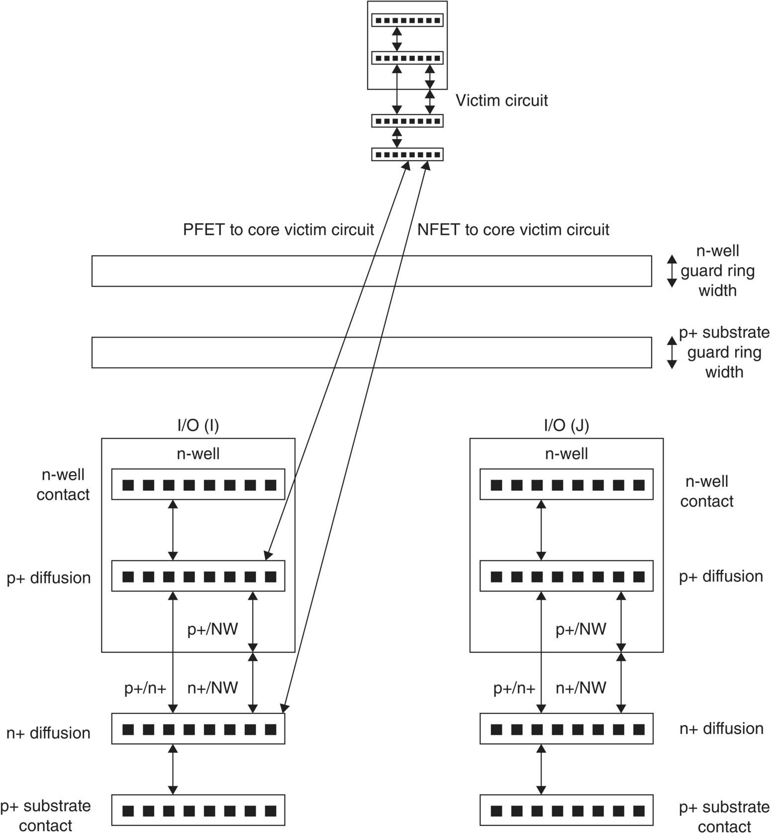
Figure 10.12 I/O to core test structure for evaluation of external latchup between I/O and core networks.
10.9 Core-to-Core Analog–Digital Floor Planning
In a semiconductor chip, the analog and digital core floor planning is key to prevent the digital noise from impacting analog circuitry. Spatial separation of the circuits and signal lines is critical as well as isolation using moats and guard rings.
10.9.1 Analog–Digital Moats and Guard Rings
Within a MS chip, analog and digital domains are physically separated to avoid digital noise and injection from affecting analog circuitry. Figure 10.13 is an example of MS floor plan. The digital and analog domains are separated by establishing a “moat.” The physical spacing between the digital and analog domains can be moat widths on the order of 10–50 µm.

Figure 10.13 Analog and digital domains with moat isolation.
10.10 High-Voltage Guard Rings
Within an LDMOS technology, there are a significant number of design layers which allow for utilization for guard rings and noise isolation [28–31]. Figure 10.14 shows an example of guard rings that contain deep implant layers to provide an improved collection of minority carriers in the substrate. With the deep implants, the guard ring efficiency is improved. With improved guard ring efficiency, noise and latchup can be reduced in CMOS analog circuitry.
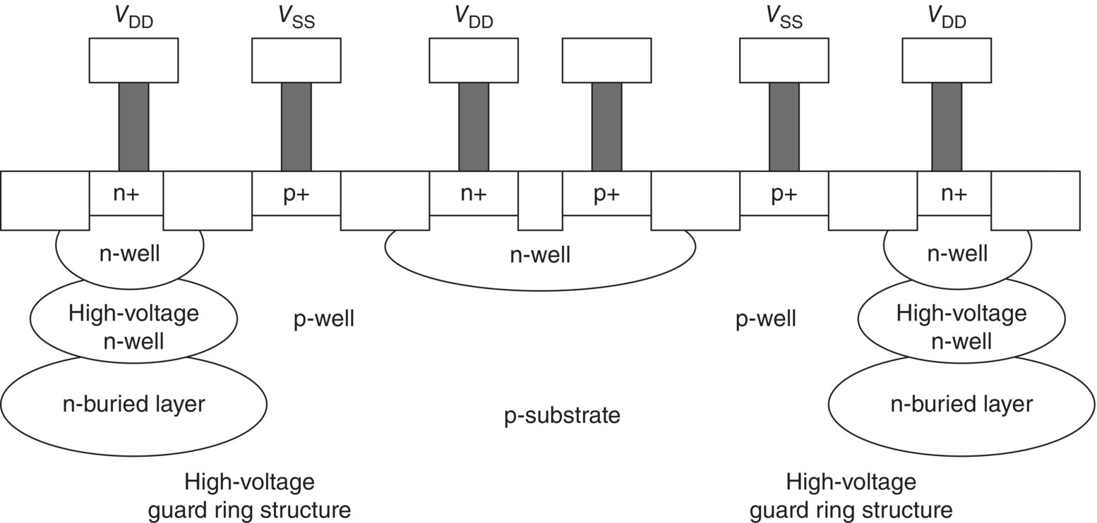
Figure 10.14 High-voltage guard ring structure with high voltage n-well implant and n-buried layer.
Figure 10.15 contains a semiconductor chip floor plan which contains high-voltage, digital, and analog domains. The high-voltage domain is spatially separated from the analog circuitry by the digital domain, as well as two moats.
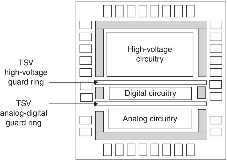
Figure 10.15 Floorplan for high voltage, digital and analog function with through silicon via (TSV).
10.11 Through-Silicon Via (TSV)
TSV structures have been introduced in advanced technologies for multichip integration. TSV structures have been integrated into silicon chips and silicon interposers. In MS chips, where digital and analog functions are on the same semiconductor chip, TSV can be used between the two domains to provide noise isolation and minimize minority carrier injection [32–39]. Figure 10.16 shows an example of a TSV guard ring structure. Figure 10.17 shows a cross section of the wafer highlighting the TSV depth extends from the top to the bottom of the wafer. TSV structures can be placed in the moat area between the digital and analog domains, allowing collection of the minority carriers and eliminating external latchup.

Figure 10.16 TSV guard ring.
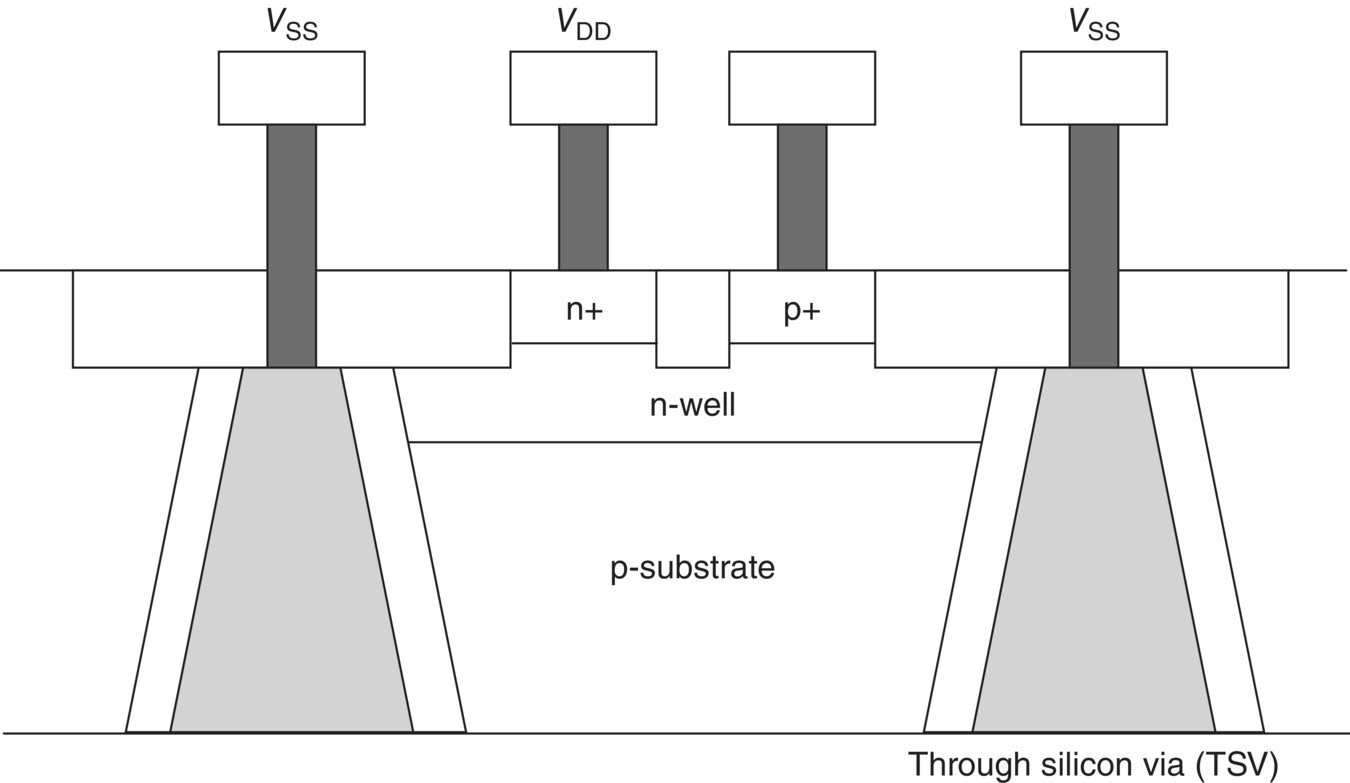
Figure 10.17 Wafer cross section of a TSV.
10.12 Trench Guard Rings
Deep trench structures can be utilized to improve the latchup robustness and noise reduction in CMOS, BiCMOS, and LDMOS technologies [40–46]. Deep trench structures are used for high-performance bipolar transistors. Deep trench structures reduce collector to substrate capacitance in bipolar transistors; these can be utilized for noise reduction and latchup. Deep trench structures can be used for guard rings (Figures 10.18 and 10.19). Deep trench structures can be on the order of 5–10 µm deep from the silicon surface. Deep trench structures prevent lateral minority carrier transport.

Figure 10.18 Deep trench guard ring.
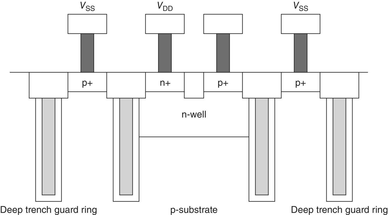
Figure 10.19 Independent guard ring structure.
10.13 Active Guard Rings
Today, SOC solutions have been used for solving the MS requirements. SOC applications have a wide range of power supply conditions, number of independent power domains, and circuit performance objectives. Different power domains are established between digital and analog circuits on an integrated chip. The integration of different circuits and system functions into a common chip has also resulted in solutions for ensuring that noise from one portion or circuit of the chip does not affect a different circuit within the chip.
With the chip integration issues, the need for better guard rings and alternative guard ring solutions has had increased interest [47–59]. Since 2000, there has been an increased focus on guard ring solutions that achieve the following objectives:
- Solutions that achieve noise isolation, latchup robustness, and ESD results
- Solutions which do not inject current back into the power grid
With the growth of interaction between digital and analog domains, new guard ring concepts have increased in importance. In addition, with the growth of smart power technology, solutions are needed for avoidance of interaction of the high-voltage CMOS (HVCMOS) chip sectors and the low-voltage sectors of a CMOS chip.
Different “active” guard ring circuit concepts have been introduced for latchup improvement. In “active” guard rings, the objective is to not only collect minority carriers but to actively compensate the effect. The latchup circuit design discipline includes the following concepts:
- Electrically collecting minority carriers at a metallurgical junction and whose junction is electrically connected to the chip substrate to alter the substrate potential
- Electrically collecting minority carriers at a metallurgical junction and whose junction is electrically connected to the chip substrate, to alter the substrate potential, with the objective of reduced forward bias of the injection structure
- Electrically collecting minority carriers at a metallurgical junction and whose junction is electrically connected to the chip substrate, to alter the substrate potential, with the objective of introduction of a lateral electrical field assist to reduce the lateral bipolar current gain
- Electrically sensing the substrate potential drop and inverting the polarity of the potential drop using inverting amplifier networks
Figure 10.20 is an example of an active guard ring. Typically, in a passive guard ring concept, a p+ substrate contact is electrically connected to a VSS power rail, and an n-well ring is electrically connected to a VDD power rail. But in an active guard ring, an n-well region is not electrically connected to a power rail. In an active guard ring, the n-well structure collects the minority carrier electrons in its metallurgical junction formed with the p-substrate region. The n-well ring is electrically connected to a “soft grounded” p+ substrate contact. When the minority carrier electrons traverse the metallurgical junction, it reduces the electrical potential of the n-well region (e.g., denoted in the figure as ΔV). By electrically connecting the n-well to the p+ substrate contact, the electrical potential of the substrate is also lowered by the same potential magnitude. In this case, the electrical potential of the region is lowered. The lowering of the substrate potential can be utilized as two means. First, given the p+ diffusion is near a forward-bias structure (e.g., an injecting structure), the reduction of the potential can lower the forward-bias state, turning off the injection process. Second, given another p+ substrate contact, a lateral electric field can be established which inhibits the flow of minority carriers. Given a parasitic npn bipolar transistor is formed between the injection source and a collecting victim circuit, if the lateral electrical field opposes the current transport, the lateral npn bipolar current gain is reduced.

Figure 10.20 N+ injection source with active and passive guard rings.
Figure 10.21 demonstrates the “electric field assist” wherein in this case, the electric field reduces the lateral bipolar current gain. In this methodology, the placement of the p+ region can be on the injection side or collection side of the n-well region. By adding an additional p++ substrate diffusion inside of the n-well ring/p+ substrate contact, a well defined electric field is established. A p+ region is flanking both sides of the n-well ring, with an outer p+ substrate contact electrically connected to the n-well ring.

Figure 10.21 N-well Injection source with active guard ring.
Figure 10.22 introduces a secondary p+ passive guard ring. Various implementations of guard rings are utilized where a plurality of p+ substrate contacts and n-wells are integrated, mixing both the active and passive concepts, where some of the wells are “floating” and some electrically connected to the power supplies. In these implementations, a plurality of trench structures can also be added to reduce the lateral bipolar current gain. In all cases, as the number of additional guard rings is increased, as well as the effective base width, the bipolar current gain decreases.
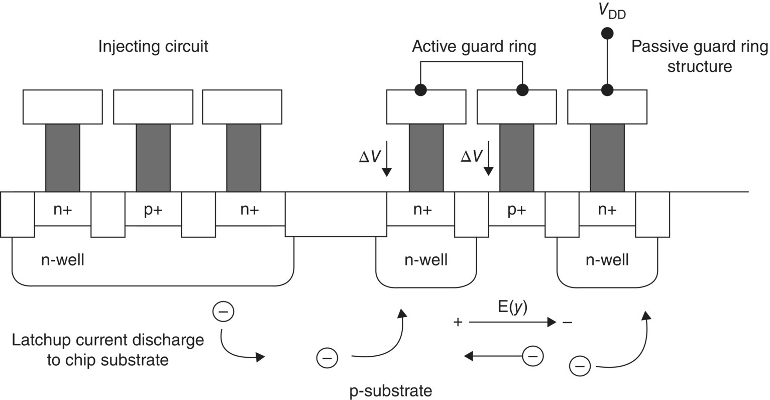
Figure 10.22 Active guard rings and secondary passive ring structure.

Figure 10.23 Active and passive guard ring structures for high voltage applications.
10.14 Closing Comments and Summary
In this chapter, latchup in analog design was discussed. This chapter addressed solutions to avoid digital noise from impacting analog circuitry. Solutions such as spatial placement of digital and analog cores in a mixed-signal chip as well as guard rings between the domains are discussed. Moats, guard rings, and TSV advantages and disadvantages are discussed as possible solutions to minimize both noise and latchup are highlighted. Special features, such as grounded wells, and decoupling capacitor issues and how they can lead to latchup in analog applications are also reviewed. In conclusion, I/O-to-I/O interactions as a function of standard cell-to-standard cell spacings were discussed. As technology spacings are reduced, cell-to-cell latchup will increase in importance in analog design.
In Chapter 11, ESD and EOS libraries and documents for an analog or MS technology are discussed. The discussion includes a plethora of items, from analog libraries, ESD library elements, Cadence-based parameterized cells, and Cadence-based hierarchical ESD designs to ESD cookbooks.
References
- 1. R. Troutman. Latchup in CMOS Technology: The Problem and Its Cure. New York: Springer, 1985.
- 2. S. Voldman. Latchup. Chichester, UK: John Wiley & Sons, Ltd, 2007.
- 3. M.D. Ker and S.F. Hsu. Transient-Induced Latchup in CMOS Integrated Circuits. Hoboken, NJ: John Wiley & Sons, Inc., 2009.
- 4. S. Voldman. Electrical Overstress (EOS): Devices, Circuits, and Systems. Chichester, UK: John Wiley & Sons, Ltd, 2013.
- 5. Y. Huh, K. Min, P. Bendix, V. Axelrad, R. Narayan, J.W. Chen, L.D. Johnson, and S. Voldman. Chip level layout and bias considerations for preventing neighboring I/O cell interaction-induced latchup and inter-power supply latchup in advanced CMOS technologies. Proceedings of the Electrical Overstress/Electrostatic Discharge (EOS/ESD) Symposium, 2005; 100–107.
- 6. S. Voldman. Latchup I/O to I/O adjacency issues in peripheral I/O design for digital and analog applications. Proceedings of the International Conference Semiconductor and Circuit Technology (ICSICT), 2012.
- 7. S. Voldman. ESD and latchup considerations for analog and power applications. Proceedings of the International Conference Semiconductor and Circuit Technology (ICSICT), 2012.
- 8. R.R. Troutman. Epitaxial layer enhancement of n-well guard rings for CMOS circuits. IEEE Electron Device Letters, 4 (12), 1983; 438–440.
- 9. J. Quinke. Novel test structures for the investigation of the efficiency of guard rings used for I/O latchup prevention. Proceedings on the International Conference on Microelectronic Test Structures (ICMTS), 1990; 35–40.
- 10. D. Tremouilles, M. Bafluer, G. Bertrand, and G. Nolhier. Latch-up ring design guidelines to improve electrostatic discharge (ESD) protection scheme efficiency. IEEE Journal of Solid-State Circuits, 39 (10), 2005; 1778–1782.
- 11. S. Voldman, C.N. Perez, and A. Watson. Guard rings: Theory, experimental quantification, and design. Proceedings of the Electrical Overstress/Electrostatic Discharge (EOS/ESD) Symposium, October 2005; 131–140.
- 12. S. Voldman, C.N. Perez, and A. Watson. Guard rings: Structures, design methodology, integration, experimental results, and analysis for RF CMOS and RF mixed signal silicon germanium technology. Journal of Electrostatics, 64, 2006; 730–743.
- 13. D. Tremouilles, M. Scholz, G. Groseneken, M.I. Natarajan, N. Azilah, M. Bafluer, M. Sawada, and T. Hasebe. A novel method for guard ring efficiency assessment and its applications for ESD protection design and optimization. Proceedings of the International Reliability Physics Symposium (IRPS), 2007; 606–607.
- 14. T. Cavioni, M. Cecchetti, M. Muschitiello, G. Spiazzi, I. Vottre, and E. Zanoni. Latch-up characterization in standard and twin-tub test structures by electrical measurements, 2-D simulations and IR microscopy. Proceedings on the International Conference on Microelectronic Test Structures (ICMTS), 1990; 41–46.
- 15. C. Mazure, W. Reczek, D. Takacs, and J. Winnerl. Improvement of latching hardness by geometry and technology tuning. IEEE Transactions on Electron Devices, ED-35 (10), 1988; 1609–1615.
- 16. Y. Song, J.S. Cable, K.N. Vu, and A.A. Witteles. The dependence of latchup sensitivity on layout features in CMOS integrated circuits. IEEE Transactions of Nuclear Science, NS-33 (6), 1986; 1493–1498.
- 17. R. Lohia and A. Ali. Parametric formulation of CMOS latchup as a function of chip layout parameters. IEEE Journal of Solid State Circuits, 23 (1), February 1988; 245–250.
- 18. R. Menozzi, L. Selmi, E. Sangiorgi, G. Crisenza, T. Cavioni, and B. Ricco. Layout dependence of CMOS latchup. IEEE Transactions on Electron Devices, ED-35 (11), 1988; 1892–1901.
- 19. M.D. Ker and J.J. Peng. Layout design and verification for cell library to improve ESD/latchup reliability in deep-submicron CMOS technology. IEEE Custom Integrated Circuit Conference (CICC), 1998; 537–540.
- 20. T. Aoki. A practical high-latchup immunity design methodology for internal circuits in the standard cell-based CMOS/BiCMOS LSI’s. IEEE Transactions on Electron Devices, 40 (8), August 1993; 1432–1436.
- 21. B. Basaran, R.A. Rutenbar, and L.R. Carley. Latchup-aware placement and parasitic-bounded routing of custom analog cells. IEEE International Conference on Computer Aided Design, 1993; 415.
- 22. H. de La Rochette, G. Bruguier, J.M. Palau, and J. Gasiot. The effect of layout modification on latchup triggering in CMOS by experimental and simulation approaches. IEEE Transaction on Nuclear Science, 41 (6), December 1994; 2222.
- 23. S. Bhattacharya, S. Banerjee, J. Lee, A. Tasch, and A. Chatterjee. Design issues for achieving latchup-free, deep trench-isolated, bulk, non-epitaxial, submicron CMOS. Proceedings of the International Electron Device Meeting (IEDM), 1990; 185–188.
- 24. M.D. Ker, W.Y. Lo, and C.Y. Wu. New experimental methodology to extract compact layout rules for latchup prevention in bulk CMOS IC’s. Proceedings of the IEEE Custom Integrated Circuits Conference (CICC), 1999; 143–146.
- 25. M.D. Ker and J.J. Peng. Layout design and verification for cell library to improve ESD/latchup reliability in deep-submicron CMOS technology. Proceedings of the IEEE Custom Integrated Circuits Conference (CICC), 1998; 537–540.
- 26. S. Voldman. Methodology for placement based on circuit function and latchup sensitivity. U.S. Patent No. 8,108,822, January 31, 2012.
- 27. S. Voldman. Latch-up analysis and parameter modification. U.S. Patent No. 6,996,786, February 7, 2006.
- 28. S. Voldman. Structure, structure and method of latch-up immunity for high and low voltage integrated circuits. U.S. Patent No. 8,519,402, August 27, 2013.
- 29. S. Voldman. Semiconductor structure and method of designing semiconductor structure to avoid high voltage initiated latch-up in low voltage sectors. U.S. Patent No. 8,423,936, August 27, 2013.
- 30. S. Voldman. Guard ring structures for high voltage CMOS/low voltage CMOS technology using LDMOS (lateral double-diffused metal oxide semiconductor) device fabrication. U.S. Patent No. 8,110,853, February 7, 2012.
- 31. S. Voldman. Structure and method for latchup improvement using wafer via latchup guard ring. U.S. Patent No. 7,989,282, August 2, 2011.
- 32. S. Voldman. Structure and method for latchup improvement using wafer via latchup guard ring. U.S. Patent No. 8,390,074, March 5, 2013.
- 33. P. Chapman, D.S. Collins, and S. Voldman. Structure and method for latchup robustness with placement of through wafer via within CMOS circuitry. U.S. Patent No. 8,420,518, April 16, 2013.
- 34. S. Voldman. ESD network circuit with a through wafer via structure and a method of manufacture. U.S. Patent No. 8,232,625, July 31, 2012.
- 35. P. Chapman, D.S. Collins, and S. Voldman. Structure and method for latchup robustness with placement of through wafer via within CMOS circuitry. U.S. Patent No. 8,017,471, September 13, 2011.
- 36. P. Chapman, D.S. Collins, and S. Voldman. Structure for a latchup robust array I/O using through wafer via. U.S. Patent No. 7,855,420, December 21, 2010.
- 37. P. Chapman, D.S. Collins, and S. Voldman. Latchup robust array I/O using through wafer via. U.S. Patent No. 7,741,681, June 22, 2010.
- 38. P. Chapman, D.S. Collins, and S. Voldman. Structure for a latchup robust gate array using through wafer via. U.S. Patent No. 7,696,541, April 13, 2010.
- 39. P. Chapman, D.S. Collins, and S. Voldman. Latchup robust gate array using through wafer via. U.S. Patent No. 7,498,622, March 3, 2009.
- 40. A. Watson, S. Voldman, and T. Larsen. Deep trench guard ring structures and evaluation of the probability of minority carrier escape for ESD and latchup in advanced BiCMOS SiGe technology. Proceedings of the Taiwan Electrostatic Discharge Conference (T-ESDC), 2003; 97–103.
- 41. S. Voldman and A. Watson. The influence of deep trench and substrate resistance on the latchup robustness in a BiCMOS silicon germanium technology. Proceedings of the International Reliability Physics Symposium (IRPS), 2004; 135–142.
- 42. S. Voldman and A. Watson. The influence of polysilicon-filled deep trench and sub-collector implants on latchup robustness in RF CMOS and BiCMOS SiGe technology. Proceedings of the Taiwan Electrostatic Discharge Conference (T-ESDC), 2004; 15–19.
- 43. S. Voldman. The influence of a novel contacted polysilicon-filled deep trench (DT) biased structure and its voltage bias state on CMOS latchup. Proceeding of the International Reliability Physics Symposium (IRPS), 2006; 151–158.
- 44. C.N. Perez and S. Voldman. Method of forming a guard ring parameterized cell structure in a hierarchical parameterized cell design, checking and verification system. U.S. Patent No. 7,350,160, March 25, 2008.
- 45. C.N. Perez and S. Voldman. Method of displaying a guard ring within an integrated circuit. U.S. Patent No. 7,350,160, March 25, 2008.
- 46. V. Parthasarathy, R. Zhu, V. Khemka, T. Roggenbauer, A. Bose, P. Hui, P. Rodriguez, J. Nivison, D. Collins, Z. Wu, I. Puchades, and M. Butner. A 0.25-µm CMOS based 70 V smart power technology with deep trench for high-voltage isolation. International Electron Device Meeting (IEDM) Technical Digest, 2002; 459–462.
- 47. M. Bafluer, J. Buxo, M.P. Vidal, P. Givelin, V. Macary, and G. Sarrabayrouse. Application of a floating well concept to a latchup-free low-cost smart power high-side switch technology. IEEE Transactions on Electron Devices, ED-40 (7), July 1993; 1340–1342.
- 48. R. Peppiette. A new protection technique for ground recirculation parasitics in monolithic power IC’s. Sanken Technical Report, 26 (1), 1994; 91–97.
- 49. M. Bafluer, M.P. Vidal, J. Buxo, P. Givelin, V. Macary, and G. Sarrabayrouse. Cost-effective smart power CMOS/DMOS technology: design methodology for latchup immunity. Analog Integrated Circuits and Signal Processing, 8 (3), November 1995; 219–231.
- 50. W.W.T. Chan, J.K.O. Sin, and S.S. Wong. A novel crosstalk isolation structure for bulk CMOS power IC’s. IEEE Transactions on Electron Devices, ED-45 (7), July 1998; 1580–1586.
- 51. W. Winkler and F. Herzl. Active substrate noise suppression in mixed-signal circuits using on-chip driven guard rings. Proceedings of the IEEE 2000 Custom Integrated Circuits Conference, May 2000; 356–360.
- 52. O. Gonnard and G. Charitat. Substrate current protection in smart power IC’s. Proceedings of the International Symposium on Power Semiconductor Devices (ISPSD), 2000; 169–172.
- 53. R. Zhu, V. Parthasarathy, V. Khemka, and A. Bose. Implementation of high-side, high-voltage RESURF LDMOS in a sub-half micron smart power technology. Proceedings of the International Symposium on Power Semiconductor Devices (ISPSD), 2001; 403–406.
- 54. O. Gonnard, G. Charitat, P. Lance, M. Susquet, M. Bafluer, and J.P. Laine. Multi-ring active analogic protection (MAAP) for minority carrier injection suppression in smart power IC’s. Proceedings of the International Symposium on Power Semiconductor Devices (ISPSD), 2001; 351–354.
- 55. M. Schenkel, P. Pfaffli, W. Wilkening, D. Aemmer, and W. Fichtner. Transient minority carrier collection from substrate in smart power design. Proceedings of the European Solid State Device Research Conference (ESSDERC), 2001; 411–414.
- 56. V. Parthasarathy, V. Khemka, R. Zhu, I. Puchades, T. Roggenbauer, M. Butner, P. Hui, P. Rodriquez, and A. Bose. A multi-trench analog + logic protection (M-TRAP) for substrate crosstalk prevention in a 0.25-µm smart power platform with 100 V high-side capability. Proceedings of the International Symposium on Power Semiconductor Devices (ISPSD), 2004; 427–430.
- 57. J.P. Laine, O. Gonnard, G. Charitat, L. Bertolini, and A. Peyre-Lavigne. Active pull-down protection for full substrate current isolation in smart power IC’s. Proceedings of the International Symposium on Power Semiconductor Devices (ISPSD), 2003; 273–276.
- 58. V. Khemka, V. Parthasarathy, R. Zhu, A. Bose, and T. Roggenbauer. Trade-off between high-side capability and substrate minority carrier injection in deep sub-micron smart power technologies. Proceedings of the International Symposium on Power Semiconductor Devices (ISPSD), 2003; 241–244.
- 59. W. Horn. On the Reverse-Current Problem in Integrated Smart Power Circuits. Ph.D. Thesis, Technical University of Graz, Austria, April 2003.