
7
Analog-ESD Signal Pin Co-synthesis
7.1 Analog Signal Pin
Receiver circuits are very important in analog electrostatic discharge (ESD) design because of the ESD sensitivity of these networks [1–7]. Typically, the analog receiver circuits are the most sensitive circuits in a chip application. Receiver performance has a critical role in the semiconductor chip performance. The primary reasons for this are as follows:
- Analog receiver circuits are small in physical area.
- Analog performance requirements limit the ESD loading allowed on the receiver. MOSFET gate area, bipolar emitter area, and electrical interconnect wiring widths impact the receiver performance.
- Analog receiver inputs are electrically connected to either MOSFET gate (in a CMOS receiver) where the MOSFET gate dielectric region is the most ESD-sensitive region in RF MOSFET receiver networks. RF MOSFET gate dielectric scales with the RF performance objectives.
- Analog receiver inputs are electrically connected to the bipolar base region (in a bipolar receiver) where the bipolar transistor emitter–base junction is the most ESD-sensitive region of the bipolar transistor. The base region scales with RF performance objectives.
- Both the MOSFET gate dielectric region and the bipolar transistor base region are the more sensitive region of the structures.
- Analog receivers require low series resistance.
Analog signal pins will require ESD protection on a semiconductor chip to protect from physical damage [1–10]. Cosynthesis of the analog functional circuit and the ESD protection provides improved optimization for the analog function [10, 11]. Within a semiconductor chip, the analog circuit may have multiple instances of an identical circuit. For some applications, these signal pin outputs are connected to a common circuit.
A challenge for today’s analog applications is to provide differential pair receiver circuitry. The challenges today in differential pair circuitry are:
- Matching
- Low capacitance
For ESD protection, the challenges are twofold:
- Signal pin-to-rail ESD protection
- Differential pair pin-to-pin ESD protection
In some analog applications, it is important to have matching characteristics. Due to across chip linewidth variation (ACLV), spatial separation of these circuits can lead to process-induced global variations. In these implementations, global variations can also occur in the ESD networks that are electrically connected to the analog signal pins. ACLV global variations and orientation can lead to variations in both the analog circuit and ESD network. Receiver circuits require low capacitance loading for high-speed applications. Receiver circuits are typically small and hence sensitive to ESD and EOS events. With the spatial separation, signal pin-to-signal pin ESD failure is not a critical issue.
As semiconductor products are scaled, power bus and electrical connections to ESD networks are scaled in ASICs, standard cell foundry design, and memory products. In the past, bus resistance was an ESD design issue between the ESD input circuit element and the ESD power clamp element.
These issues will be discussed in the following sections, as well as solutions to improve these issues using common centroid design practices as well as in combination with parasitic elements. In this chapter, we will introduce the concept of using a common centroid for the circuit, the signal pin-to-rail ESD, and then codesign and cosynthesis of the differential pair pin-to-pin ESD protection.
7.2 Analog Signal Differential Receiver
In analog differential circuits, at least two signal lines are connected to a common analog circuit [3–8]. In differential circuits, the signal lines and elements within the circuit are closely spaced. Differential circuits are sensitive to local process-induced variations that can impact the matching of resistor, capacitor, and transistor elements.
7.2.1 Analog Signal CMOS Differential Receivers
Figure 7.1 shows an example of a CMOS differential pair circuit with signal pin ESD networks [3–6]. In practice, these circuits are small and hence sensitive to ESD events. ESD testing of differential circuits requires an ESD pin-to-rail test (e.g., signal pin to VDD and signal pin to VSS), as well as a signal pin-to-signal pin test. In a differential pair circuit, where there is adjacency of elements connected to bond pads, ESD failure due to signal pin-to-signal pin ESD events can lead to low ESD results of the analog semiconductor chip. Figure 7.2 shows a solution for both signal pin-to-rail ESD protection and pin-to-pin ESD networks. The ESD signal pin-to-pin network must be bidirectional and symmetric.

Figure 7.1 Differential input schematic with signal pin ESD.

Figure 7.2 CMOS differential pair analog circuit schematic with signal pin ESD and pin-to-pin ESD.
Figure 7.3 shows a solution for both signal pin-to-rail human body model (HBM) and charged device model (CDM) ESD protection and pin-to-pin ESD networks. In analog applications with small semiconductor chips, CDM failure levels are significantly lower. In mixed-signal analog-to-digital semiconductor chips, it is a larger concern due to the charge storage of the larger semiconductor chip.
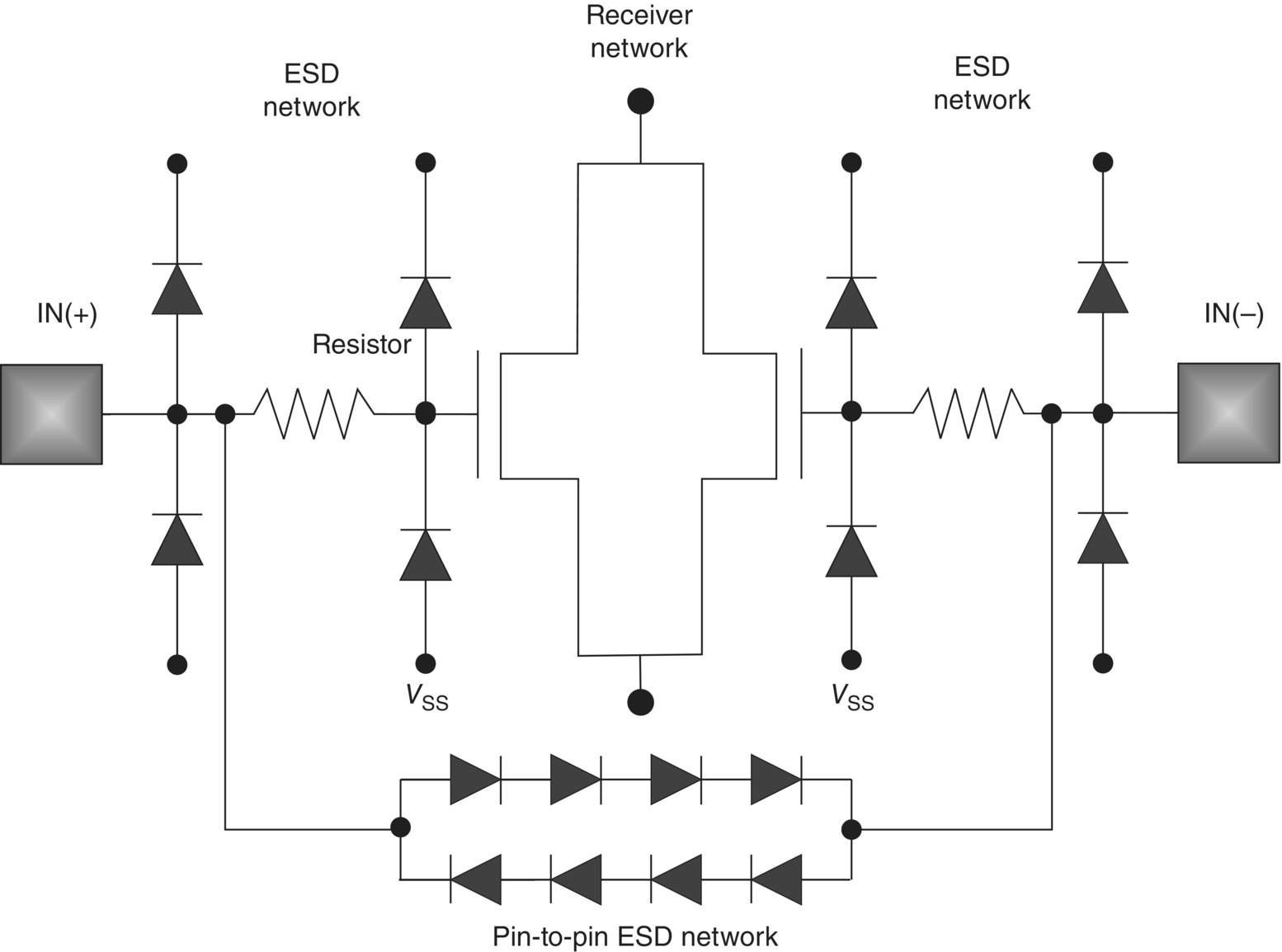
Figure 7.3 CMOS differential pair analog circuit schematic with signal pin HBM and CDM ESD and pin-to-pin ESD.
7.2.2 Analog Signal Bipolar Differential Receivers
Bipolar technology can also be used for differential pair receiver circuits [4]. Figure 7.4 is an example of a bipolar differential pair analog circuit. In the case of MOSFETs, the current does not flow through the differential pair transistors due to the MOSFET gate dielectric that is connected to the signal pins. But, in bipolar differential pair circuitry, current can flow into the metallurgical junction of the base–emitter and base–collector of the npn transistors. Receiver circuits are a common ESD-sensitive circuit in bipolar and bipolar-CMOS (BiCMOS) technology. Bipolar receiver circuits typically consist of npn bipolar transistor configured in a common emitter configuration (Figure 7.4). For bipolar receivers, the input pad is electrically connected to the base contact of the npn transistor, with the collector connected to VCC either directly or through additional circuitry. The npn bipolar transistor emitter is electrically connected to VSS, or through an emitter resistor element, or additional circuitry.
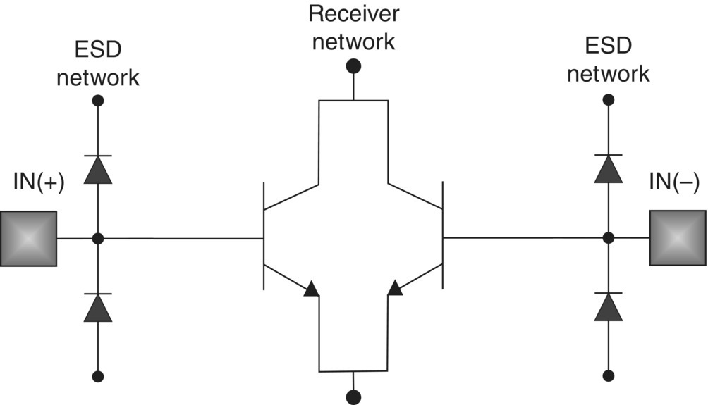
Figure 7.4 Bipolar differential pair analog circuit schematic with signal pin ESD.
One of the unique problems with differential receiver networks is pin-to-pin ESD failure mechanisms. In ESD testing, we can apply an ESD pulse event to one of the two differential signal pads and use the second differential signal pad as the ground reference. In differential pair bipolar receiver networks, for positive polarity HBM ESD events, as the base voltage increases, the base–emitter voltage of the first transistor increases, leading to forward biasing of the base–emitter junction. The base–emitter junction becomes forward active, leading to current flowing from the base to the emitter region. For the second npn bipolar transistor, the base–emitter region is reverse biased. As the voltage on the first signal pad increases, the base–emitter reverse-bias voltage across the second transistor base–emitter metallurgical junction increases.
In bipolar receiver networks, for positive polarity HBM ESD events, as the base voltage increases, the base–emitter voltage increases, leading to forward biasing of the base–emitter junction. The base–emitter junction becomes forward active, leading to current flowing from the base to the emitter region. Typically in bipolar receiver networks, the physical size of the emitter regions is small. When the ESD current exceeds the safe operating area (SOA), degradation effects occur in the bipolar transistor. The bipolar device degradation is observed as a change in the transconductance of the bipolar transistor. From the electrical parametrics, the unity current cutoff frequency, fT, decreases with increased ESD current levels. From a fT–IC plot, the fT magnitude decreases with ESD pulse events, leading to a decrease in the peak fT. Avalanche breakdown occurs in the emitter–base metallurgical junction, leading to an increase in the current flowing through the emitter and base regions; this leads to thermal runaway and second bipolar breakdown in the grounded second bipolar transistor of the differential pair. Note that the degradation of the second transistor prior to the first transistor can also lead to a differential offset hampering the matching of the two sides of the differential pair. It is possible that the failure criterion is associated with an npn mismatch prior to the ESD failure of either npn device (Figure 7.5).

Figure 7.5 Current path for pin-to-pin test for bipolar differential pair receiver with only signal pin ESD.
For a negative pulse event, the base–emitter region is reverse biased. As the voltage on the signal pad decreases, the base–emitter reverse-bias voltage across the base–emitter metallurgical junction increases. Avalanche breakdown occurs in the emitter–base metallurgical junction, leading to an increase in the current flowing through the emitter and base regions; this leads to thermal runaway and second bipolar breakdown in the bipolar transistor. The experimental results show that the negative polarity failure level has a lower magnitude compared to the positive polarity failure level.
An ESD design solution used to provide improved ESD results in a differential pair bipolar receiver network is to place a p–n diode element in parallel with the npn bipolar transistor emitter–base junction (Figure 7.6). Using a parallel element, the p–n junction is placed such that the anode is electrically connected to the npn emitter and the cathode to the base region. In this fashion, an alternate forward-bias current path is established between both sides of the differential pair. Figure 7.7 shows the current path through the differential pair emitter–base and the additional diode element.

Figure 7.6 Bipolar differential pair analog circuit schematic with signal pin ESD and emitter–base ESD device.

Figure 7.7 Current path in bipolar differential pair analog circuit schematic with signal pin ESD and emitter–base ESD device.
An alternative method is to introduce multi-emitters within the base region of the npn transistors. Multi-emitter bipolar transistors were utilized in bipolar technology in static RAM (SRAM) memory cells. Figure 7.8 provides an example of a multi-emitter bipolar transistor, where a larger emitter is utilized for the ESD protection scheme [10].

Figure 7.8 Bipolar differential pair analog circuit schematic with signal pin ESD and with multi-emitter emitter–base ESD device.
Another method is to introduce a back-to-back diode string between both sides of the differential pair. Figure 7.9 shows a bipolar differential pair with an ESD diode string between the two sides of the differential pair. This has the advantage of allowing a higher current between both sides of the differential pair and avoiding emitter–base degradation but has the disadvantage of asymmetry matching and capacitance loading performance degradation.

Figure 7.9 Bipolar differential pair analog circuit schematic with signal pin ESD and pin-to-pin ESD protection.
7.3 Analog CMOS Differential Receiver
In standard CMOS differential receiver design, ESD elements are associated with each signal pad, as well as an ESD signal pin-to-signal pin between the signal pads (Figure 7.10). In the implementation layout, ESD device is placed on each bond pad. The ESD elements are spatially separate, leading to design mismatch. Design layout solutions are achieved by establishing common centroid design layout practices used in analog design. Sources of mismatch can occur due to the separation of the ESD pin-to-rail networks as well as the signal pin-to-signal pin ESD networks. Figure 7.10 is an example of a CMOS differential pair with ESD network for signal pin-to-rail and signal pin-to-signal pin ESD network. Figure 7.10 shows a standard practice of a differential pair circuit with both ESD pin-to-rail protection network and ESD pin-to-pin protection networks. With the addition of the differential pair pin-to-pin ESD networks, there is both an area and loading impact to the differential pair circuit performance. In addition, without a common centroid implementation, it will introduce a mismatch [4–7].

Figure 7.10 Standard practice for ESD pin-to-pin network for differential pair circuits.
7.3.1 Analog Differential Receiver Capacitance Loading
A second issue, given that either diode, MOSFET, or SCR ESD networks are used, the loading capacitance of the ESD network impacts differential pair receiver performance. In the case of a dual-diode ESD network, two additional diode capacitances are added to the differential pair network for both IN(+) and IN(−). This common centroid concept is typically not extended to ESD networks.
7.3.2 Analog Differential Receiver ESD Mismatch
ESD signal pin-to-rail protection networks impact the mismatch and loading capacitance of the differential pair circuitry. The first critical issue is the mismatch introduced between the two sides of the differential pair from the ESD structure itself. With the addition of the ESD network on the IN(+) and second ESD network on IN(−), a mismatch occurs since both ESD networks are spatially separated. Hence, the spatial separation of the two separate ESD networks can lead to functional implications in itself (Figure 7.11).

Figure 7.11 Placement of analog differential pair ESD circuits without common well.
Symmetry is important for minimizing design variation for both circuits and ESD networks [9]. A metric to define symmetry is by establishing an axis of symmetry. Figure 7.12 demonstrates a common centroid in analog differential pair networks [9].

Figure 7.12 Common centroid for analog circuit with ESD.
Common centroid design introduces four rules: (1) coincidence, (2) symmetry, (3) dispersion, and (4) compactness [9]. To minimize variations, symmetry can be evaluated in one dimension or both dimensions. For example, an axis of symmetry can be defined in the x-axis, and a second axis of symmetry can be defined in the y-axis. From these axes of symmetry, a common centroid can be established. Common centroid design is a process used in analog design practices. Figure 7.13 is an example of a common centroid differential pair with x- and y-symmetry [11].

Figure 7.13 Common centroid for analog circuit with x- and y-symmetry.
For the case of grounded-gate MOSFETs, common centroid design can also be utilized. Figure 7.14 shows an example of common centroid differential pair and ESD network. To provide improved matching, the two ESD networks of the differential pair can be cosynthesized with the differential circuit and share a common centroid in one or two dimensions [11]. With layout cosynthesis, the input devices and the ESD networks can share a common centroid in both the x-axis of symmetry and the y-axis of symmetry. For example, an NFET ESD network can be placed with the circuit itself (e.g., an NFET) in a common centroid fashion.

Figure 7.14 Common centroid differential pair with x- and y-symmetry for analog circuit with GGNMOS.
7.4 Analog Differential Pair ESD Signal Pin Matching with Common Well Layout
Figure 7.15 is an example where the two differential ESD elements are placed locally to each other and in a common n-well tub [11]. Normally, ESD element for IN(+) is placed at the signal pad for IN(+), and ESD element for IN(−) is placed at the signal pad for IN(−). In this example, the ESD elements are placed into a common shared region. In this case, the n-well region is common, and the spatial separation between IN(+) and IN(−) is minimum. Figure 7.15 shows one of the two diodes (e.g., P+/NW diodes), where the two ESD networks are placed in a common tub and placed locally together in a common array. Note that the second N+/PW can be designed equivalently.

Figure 7.15 Layout of common n-well ESD protection for a differential pair.
Figure 7.16 is a cross section where the two differential ESD elements are placed locally to each other and in a common n-well tub. In this example, the ESD elements are placed into a common shared region. In this case, the n-well region is common, and the spatial separation between IN(+) and IN(−) is minimum. Figure 7.16 shows one of the two diodes (e.g., P+/NW diodes), where the two ESD networks are placed in a common tub and placed locally together in a common array. Note that the second N+/PW can be designed equivalently [11].

Figure 7.16 Cross section of ESD common centroid differential with common well tub.
7.5 Analog Differential Pair Common Centroid Design Layout: Signal Pin-to-Signal Pin and Parasitic ESD Elements
ESD signal pin-to-signal pin protection networks are required to provide ESD protection from the two pins within a differential pair circuit. Typically in analog applications (e.g., CMOS and bipolar), the differential pair pins are the most sensitive pins in a given semiconductor chip. It has been also shown that in “signal pin to all other signal pins (reference ground),” the failure mechanism occurs between the two pins of the differential pair [11].
For CMOS differential pair, there are two solutions for establishing the signal pin-to-signal pin ESD networks. Presently, the established conventional method is to utilize a bidirectional ESD network between the IN(+) and IN(−). Typically, it is not a common centroid implementation.
A novel method is to introduce a common centroid implementation, where one ESD array serves both sides of the differential pair network. In this fashion, a common centroid design can be achieved. By taking the next step of alternating the fingers of the one ESD array, the parasitic elements between the two sides can be used.
For example, a lateral parasitic pnp can be formed between adjacent fingers of the differential pair ESD network p+/n-well diode. Additionally, a lateral parasitic npn can be used between adjacent fingers of the differential pair ESD network n+/p-well diode (Figure 7.17).

Figure 7.17 Differential pair interdigitated common centroid design and utilization of parasitic elements for signal pin-to-signal pin ESD protection.
This achieves multiple objectives:
- Common centroid design with improved matching
- No additional capacitance load on the differential pair receiver network
- No additional area for an additional ESD network
Figures 7.18 and 7.19 provide a cross section utilizing a differential pair with a parasitic pin-to-pin ESD element. A lateral parasitic pnp element is used to provide ESD protection between the IN(+) and IN(−) electrodes.

Figure 7.18 Differential pair interdigitated common centroid design and utilization of parasitic elements for signal pin-to-signal pin ESD protection.

Figure 7.19 Differential pair interdigitated common centroid design and utilization of parasitic elements for signal pin-to-signal pin ESD protection.
Figure 7.20 shows a high-level circuit schematic of the differential pair with a parasitic pin-to-pin ESD element. It also shows an example with the parasitic pnp. A lateral parasitic pnp element is used to provide ESD protection between the IN(+) and IN(−) electrodes [11].

Figure 7.20 Circuit schematic of differential pair with interdigitated pin-to-pin ESD devices.
Figure 7.21 shows an example with the parasitic pnpn [11]. A lateral parasitic pnpn element is used to provide ESD protection between the IN(+) and IN(−) electrodes. Figure 7.22 shows an example layout using the parasitic pnpn.

Figure 7.21 Circuit schematic of differential pair with interdigitated pin-to-pin pnpn ESD devices.
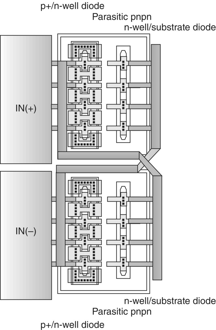
Figure 7.22 Layout of differential pair with interdigitated pin-to-pin pnpn ESD devices.
7.6 Closing Comments and Summary
This chapter addressed analog and ESD signal pin cosynthesis that introduces usage of interdigitated layout and common centroid concepts to provide ideal matching, low capacitance, and small area in differential signal pins. Using interdigitated designs, the parasitic elements are utilized for signal pin-to-signal pin ESD protection. In conclusion, the issue of common centroid design of ESD protection networks which integrates signal pin-to-signal pin ESD protection with the interdigitation pattern for ESD pin-to-rail protection network for differential pair circuitry is discussed for the first time. With integration of the ESD pin-to-rail solution and the ESD signal pin solution, a significant reduction of the area and loading effect for CMOS differential circuits is established. This novel concept will provide significant advantage for present and future high-performance analog and RF design for matching, area reduction, and performance advantages.
Chapter 8 focuses on floor planning in analog and mixed-signal chip design. Core and peripheral I/O design will be addressed associated with analog applications. Integration of analog and digital ESD networks within the semiconductor chip floor plan is quantified. ESD power clamp placement and integration for independent and master/slave implementation systems were shown. Examples of rectangular and octagonal bond and integration of circular and octagonal ESD elements are shown. The chapter closes with the current and the future issues for 2.5-D and 3-D systems.
References
- 1. V. Vashchenko and A. Shibkov. ESD Design for Analog Circuits. New York: Springer, 2010.
- 2. S. Voldman. ESD: Physics and Devices. Chichester, UK: John Wiley & Sons, Ltd, 2004.
- 3. S. Voldman. ESD: Circuits and Devices. Chichester, UK: John Wiley & Sons, Ltd, 2005.
- 4. S. Voldman. ESD: RF Circuits and Technology. Chichester, UK: John Wiley & Sons, Ltd, 2006.
- 5. S. Voldman. ESD: Failure Mechanisms and Models. Chichester, UK: John Wiley & Sons, Ltd, 2009.
- 6. S. Voldman. ESD: Design and Synthesis. Chichester, UK: John Wiley & Sons, Ltd, 2011.
- 7. S. Voldman. ESD Basics: From Semiconductor Manufacturing to Product Use. Chichester, UK: John Wiley & Sons, Ltd, 2012.
- 8. S. Voldman. Electrical Overstress (EOS): Devices, Circuits, and Systems. Chichester, UK: John Wiley & Sons, Ltd, 2013.
- 9. A. Hastings. The Art of Analog Layout. Upper Saddle River, NJ: Prentice Hall, 2006.
- 10. S. Voldman. Dual emitter transistor with ESD protection. U.S. Patent No. 6,731,488, May 4, 2004.
- 11. S. Voldman. Common centroid differential pair signal pin-to-signal pin analog ESD design. Proceedings of the IEEE 11th International Conference on Solid-State and Integrated Circuit Technology (ICSICT), 2012.