
2
Analog Design Layout
2.1 Analog Design Layout Revisited
In analog design, unique design practices are used to improve the functional characteristics of analog circuitry [1–10]. In the electrostatic discharge (ESD) design synthesis of analog circuitry, the ESD design practices must be suitable and consistent with the needs and requirements of analog circuitry [11]. Fortunately, many of the analog design practices are aligned with ESD design practices [12–18]. In the analog design discipline, there are many design techniques to improve tolerance of analog circuits. Analog design techniques include the following:
- Local matching: Placement of elements close together for improved tolerance
- Global matching: Placement in the semiconductor die
- Thermal symmetry: Design symmetry
A key analog circuit design requirement is matching [1]. To avoid semiconductor process variations, matching is optimized by the local placement. Placement within the die location also is an analog concern due to mechanical stress effects. In analog design, there is a concern of the temperature field within the die and the effect of temperature distribution within the die.
Many of the analog design synthesis and practices are also good ESD design practices. The design practices of matching and design symmetry are also suitable practices for ESD design. But there are some design practices where a trade-off exists between the analog tolerance and ESD; this occurs when parasitic devices are formed between the different analog elements within a given circuit or circuit to circuit.
In semiconductor development, semiconductor process variation can introduce structural and dimensional nonuniformity. Photolithography and etch tools can introduce these nonuniformities that exist on a local and global design level. These variations can manifest themselves by introducing variations in both active and passive elements. For MOSFET transistors, variation in the MOSFET channel length in single-finger and multifinger MOSFET layouts can lead to nonuniform “turn-on”; this effect can influence both active functional circuits and ESD networks. In bipolar transistors, the linewidth variation can lead to different sizes in emitter structures, leading to nonuniform current distribution in multifinger bipolar transistors. For resistor elements, resistor elements that are utilized for ballasting in multifinger structures can also lead to nonuniform current in the different fingers in the structure.
Design factors that influence the lack of variation are the following semiconductor process and design variables:
- Linewidth
- Line-to-line space
- “Nested-to-isolated” ratio
- Orientation
- Physical spacing between identical circuits
It is an analog circuit design practice and an ESD design synthesis practice to provide a linewidth which is well controlled. For line-to-line space, in an array of lines, the spacing is maintained to provide maximum matching between adjacent lines. For example, in a multifinger MOSFET structure, the spacing between the polysilicon lines is equal to provide the maximum matched characteristics.
Given any array of parallel lines, the characteristics of the “end” or edges of the array can have different characteristics than the other lines. In an array of lines, whereas one edge is adjacent to another line, the other edge is not; this leads to one line-to-line edge space to appear “nested” and the outside line-to-line edge space to appear “semi-infinite” or “isolated.” To address the problem of poorly matched edge lines, the following semiconductor process and ESD design solutions are used:
- Process: Cancellation technique of photolithography and etch biases
- Design: Use of dummy edge lines
- Circuit: Use of “gate-driven” circuitry
2.1.1 Analog Design: Local Matching
Analog design local matching is important for segments within a given circuit element or circuit elements within a given circuit [1]. For example, local matching is important in differential pair circuits and current mirrors. Many of the analog design matching practices are also good ESD design practices, which will be discussed.
2.1.2 Analog Design: Global Matching
Analog design global matching is important for circuits that are identical elements but physically spaced around a semiconductor chip [1]. For example, global matching is important in MUX circuits where the inputs are placed at different physical locations within a semiconductor chip. Orientation can also influence the linewidth of identical circuits both locally and globally.
On a macroscopic full-chip scale, there are variations in the photolithography and etching from the top to bottom of a semiconductor chip. In the design of a semiconductor chip, these can be compensated with a preknowledge of the photolithography and etch variations of a technology.
An ESD design practice is to maintain the same x–y orientation of ESD circuits in a semiconductor chip to minimize variation pin to pin. This is not always possible in a peripheral architecture where the ESD element is rotated on the four edges of the semiconductor chip. Note that in this case, the circuit itself (e.g., off-chip driver) may also undergo an orientation effect. It is a good ESD design synthesis practice that addresses the orientation issue with compensation and matching issues for orientation of the ESD elements (in conjunction with the circuit it is protecting).
2.1.3 Symmetry
Symmetry is important to analog design in that it can improve matching characteristics from layout variations and thermal distribution. Analog design global matching is important for circuits that are identical elements but physically spaced around a semiconductor chip.
2.1.4 Layout Design Symmetry
Symmetry is important to analog design in that it can improve matching characteristics from layout variations and thermal distribution [1]. Analog design global matching is important for circuits that are identical elements but physically spaced around a semiconductor chip.
Design symmetry is an ESD design practice to maximize the ESD robustness. The capability of the ESD network to dissipate high-current pulse events is directly related to the network’s topology and its design symmetry. The more uniform the current distribution is through the ESD network during a discharge, the better the utilization of the area of the structure, and as a consequence, the greater the robustness of the circuit design. The distribution of current during an ESD event is dependent upon the design symmetry of the ESD network and its components.
To define ESD design symmetry, an axis of symmetry can be defined in the ESD design. Semiconductor design layout is two dimensional, allowing to define an axis of symmetry in the x- and y-direction.
2.1.5 Thermal Symmetry
Thermal symmetry is important in analog design to provide matching of elements in the thermal field [1]. Thermal symmetry is important to avoid mismatch of elements. Since semiconductor element electrical and thermal parameters are temperature dependent (e.g., mobility, electrical conductivity, thermal conductivity), the more uniform the current distribution, the more symmetrical the temperature distribution within the device.
From an ESD perspective, the degree that the design of the ESD network (or structure) on all levels of the integrated circuit departs from a symmetric configuration, the greater is the current localized or nonuniformities in the ESD network. With a symmetrical distribution of the current, the peak power-to-failure per unit area is lowered, producing superior results. Additionally, the more uniform the current distribution, the more uniform the thermal field as well. In integrated circuit design, a key ESD design concept is to maintain a high degree of design symmetry within a structure on all design levels. In both the ESD network and I/O driver circuit, an evaluation of the power distribution of an ESD event within the circuit is an indicator of the robustness of the integrated circuit. Hence, physical layout design symmetry can be used as a heuristic determination of the power distribution within a physical structure.
2.2 Common Centroid Design
Common centroid design practice is used in analog circuitry to provide a high degree of matching [1]. It is commonly used in circuitry where there is a desire to have matching of two components in a circuit. The two devices can be resistors, capacitors, diodes, bipolar junction transistors (BJT), or MOSFET devices.
A typical use of common centroid layout is generally used with differential pair circuitry. It is a matching methodology in which the two transistors of the differential pair circuit are symmetrically laid out about a certain axis. In this fashion, the design style guarantees that both elements see the same semiconductor process variations, providing the best matching characteristics.
2.2.1 Common Centroid Arrays
In the common centroid design method, common centroid arrays are formed to integrate multiple devices in a common area [1]. Arrays whose common centroids align are known as common centroid arrays. Ideally, common centroid arrays eliminate systematic mismatches in the element (Figure 2.1).

Figure 2.1 Common centroid design.
2.2.2 One-Axis Common Centroid Design
Common centroid design can be introduced in one dimension or two dimensions [1]. One-dimensional common centroid design is utilized in devices which inherently have a large ratio of length to width. One-dimensional common centroid design is used in the design of resistors, MOSFET devices, and BJT devices. ESD networks which consist of MOSFETs, BJT, and resistor elements can introduce this design practice.
2.2.3 Two-Axis Common Centroid Design
Common centroid design can be introduced in two dimensions [1]. Figure 2.2 is an example of two-dimensional common centroid design. Two-dimensional common centroid design is introduced in capacitor arrays. Figure 2.3 is an example of a larger two-dimensional centroid array.

Figure 2.2 Example of two-dimensional common centroid array.

Figure 2.3 Example of a larger two-dimensional common centroid array.
2.3 Interdigitation Design
A second style of layout design for analog is known as interdigitation design layout [1]. In interdigitation layout, devices are in interleaved manner. Capacitors, resistors, diodes, and transistors can be interleaved to provide good matching characteristics and alleviate gradients. For example, given two devices, device A and device B, these can be formed into four unit cells where it is desirable to match device A and device B. This can be represented as
Given there is a gradient, these will not be matched.
Forming an axis of symmetry, highlighted as “|”, an interdigitated design layout can be shown as
Figure 2.4 shows an example of the physical layout of the interdigitation.

Figure 2.4 Example of interdigitation layout.
2.4 Common Centroid and Interdigitation Design
The two methodologies of common centroid design and interdigitation are different. First, common centroid design can be in two dimensions. Common centroid design is used when critical matching is required [1, 8, 9].
Interdigitation design layout has an axis of symmetry where two devices are interleaved. Interdigitation design layout eliminates any linear gradient. Common centroid design layout is more precise than interdigitation design but may require more area.
For common centroid design, two axes of symmetry are needed. Assuming device A and device B are divided into 16 unit devices, a common centroid structure, with two axes of symmetry, would be represented as

2.5 Passive Element Design
Common centroid design and interdigitation design methodologies can be applied to passive elements. Passive elements that utilize these practices can be used in resistors, capacitors, and even inductor elements. The choice of usage of common centroid design versus interdigitation design is a function of the need for critical matching or “good enough” matching characteristics.
2.6 Resistor Element Design
Resistor design is important in analog applications where resistor mismatch is a design issue. Analog design utilizes standard design practices, interdigitated layout design, and common centroid methodologies.
2.6.1 Resistor Element Design: Dogbone Layout
Figure 2.5 is an example of a resistor design element used in analog applications and ESD circuitry [15, 16]. The “dogbone” design style is used in circuitry where a high degree of matching is not required. Figures 2.5 and 2.6 are examples of an n-type dogbone design and p-type dogbone design, respectively [15, 16]. Dogbone design can be used for ESD input networks where the ends of the dogbone serve as diode elements. In ESD input circuitry that uses a human body model (HBM) dual diode–resistor–charged device model (CDM) dual-diode network, the end of the dogbone can serve as a CDM diode element.

Figure 2.5 ESD dogbone n-diffusion resistor.
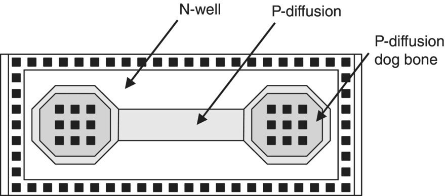
Figure 2.6 ESD dogbone p-diffusion resistor.
2.6.2 Resistor Design: Analog Interdigitated Layout
Analog applications that require good matching characteristics introduce interdigitated layout design methodologies [1]. Figure 2.4 showed an example of interdigitated design of two resistor elements. In interdigitated designs, connections between resistor segments are electrically connected using “jumpers.” Figure 2.7 shows an example of an interdigitated design with “folded-out” jumper elements. Figure 2.8 shows an example of an interdigitated design with “folded-in” jumper elements [1]. Folded-in jumper leads to the interconnect to be placed over the diffusion. For ESD events, this can lead to an increase in the temperature in the region of the interconnect.
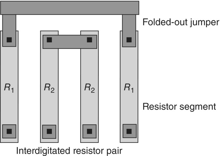
Figure 2.7 Interdigitated resistor layout—folded-out jumper.

Figure 2.8 Interdigitated resistor layout—folded-in jumper.
2.6.3 Dummy Resistor Layout
Photolithographic and etch variations can lead to width variations of segments in a resistor array. Segments on the edges of arrays can have different widths than segments in the center of an array, due to “nested-to-isolated” width variations. Analog applications that require good matching characteristics can introduce “dummy shapes” on the edges of a resistor segment array. Figure 2.9 is an example of an interdigitated layout design with dummy segments on the edges [1].
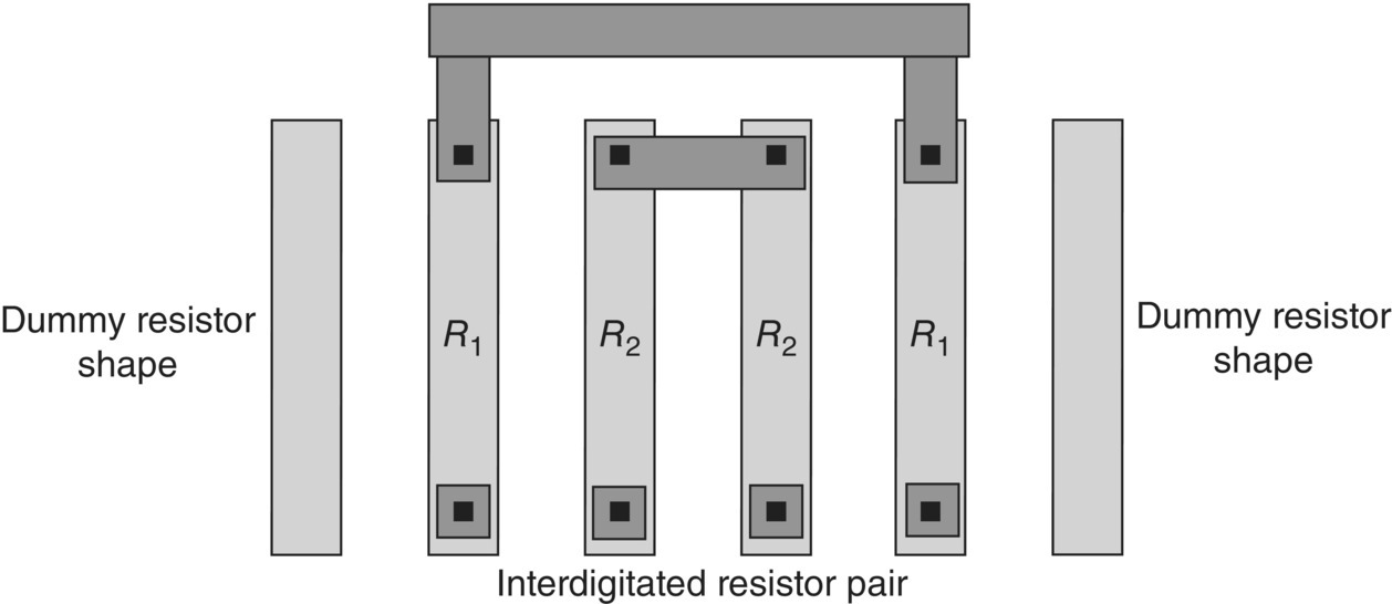
Figure 2.9 Interdigitated resistor layout with dummy resistor shapes.
In these implementations, the dummy resistor segments can be grounded, biased, or left floating; the electrical connection of the dummy shapes can lead to ESD failure mechanisms between the dummy shape segments and the resistor element.
2.6.4 Thermoelectric Cancellation Layout
The Seebeck effect, also known as the thermoelectric effect, can introduce a thermoelectric potential variation between the two ends of a segment. A thermoelectric potential is equal to the Seebeck coefficient times the temperature difference between the two ends of the resistor segment. The Seebeck coefficient is equal to typically 0.4 mV/°C where C is the degrees in Celsius [1]. Figure 2.10 shows improper connections of the segments which introduce the thermoelectric effect. A temperature variation between the top and bottom contacts can lead to a thermoelectric potential. With the proper connections between the two ends, this can be minimized. Figure 2.11 shows proper connections of the segments to eliminate the thermoelectric effect.

Figure 2.10 Thermoelectric effect in resistors due to resistor layout improper connections.
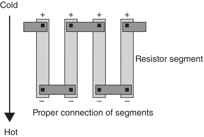
Figure 2.11 Thermoelectric cancellation resistor layout—proper connections.
2.6.5 Electrostatic Shield
Passive element voltage conditions and resistor values can be influenced by power buses and signal lines that extend over the resistor elements. A solution to avoid the voltage bias influence on the passive elements from power bus or signal lines is to introduce “electrostatic shield” or field shield [1]. Figure 2.12 shows an example of an electrostatic shield placed between the overlying power or signal lines and the passive element.
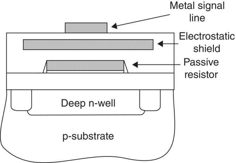
Figure 2.12 Electrostatic shield and resistor layout.
2.6.6 Interdigitated Resistors and ESD Parasitics
Interdigitated resistor elements in differential circuits can lead to parasitic interactions during ESD events. Figure 2.13 provides an example of two interdigitated resistor elements where the resistors are connected to two different signal pins. For the case of a differential pair circuit, one resistor is connected to IN(+) and the second resistor is connected to IN(−). For n-type resistors, a parasitic npn bipolar transistor can be formed between the two resistor segments. This parasitic npn transistor can lead to signal pin-to-signal pin ESD failures. At the same time, note that this parasitic npn (with proper design) can be utilized for pin-to-pin ESD protection.

Figure 2.13 Interdigitated resistor layout and ESD parasitic adjacency issue.
Resistor passive element robustness can be limited by interconnects, such as contacts, vias, and metal lines of the jumper elements. To improve the robustness of the resistor passive and jumper elements, additional contacts or vias can be added to the interdigitated resistor design. ESD failures do occur in resistor elements where a single contact is used. Figure 2.14 provides an example of interdigitated resistor elements with multiple contacts.
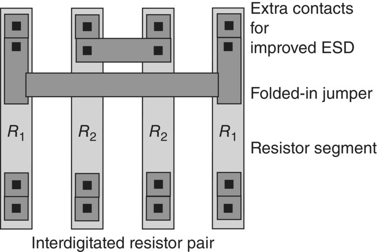
Figure 2.14 ESD robust interdigitated resistor layout with double contacts.
2.7 Capacitor Element Design
Capacitors can be designed in a two-dimensional common centroid array where critical matching is needed in analog design [1, 8, 9]. Dummy edge capacitors can be used to avoid edge effects which can influence the capacitance of the elements in the array. Figure 2.15 shows an example of a capacitor array with dummy edge capacitor elements.

Figure 2.15 Two-dimensional common centroid analog capacitor element with dummy edge capacitors.
2.8 Inductor Element Design
Inductors are used in analog and radio frequency (RF) applications [17]. On-chip inductors are used on the inputs and output of circuitry. Inductors are used in peripheral circuits for resonant circuits, baluns, and transformers and as AC current blocks (e.g., also known as AC chokes), as well as other circuit applications. High-quality factor inductors are important for analog applications. On-chip inductors in semiconductor technology are constructed from the interconnect technology. The inductors consist of conductive metal films, metal contacts, metal vias, and interlevel dielectrics. The quality factor “Q” can be defined as associated with ratio of the imaginary and real part of the self-admittance term

where, at self-resonance, can be expressed as
Assuming the quality factor “Q” for an inductor is dependent on the inductor series resistance and the inductance (ignoring capacitance effects), the Q of the inductor with a series resistance is

Figure 2.16 is an example of a rectangular inductor design. Figure 2.17 is an example of a symmetric inductor coil pair with a center tap connection. The inductor pair design provides good matching between the two inductor elements.

Figure 2.16 Rectangular inductor.

Figure 2.17 Octagonal inductor pair T-coil with center tap.
ESD failures of the inductor elements typically occur at the underpass connection, where the wire cross-sectional area is reduced for the lower-level metal layer. ESD-induced resistance shift can also lead to analog circuit mismatch. In the case that there is a permanent shift due to ESD stress in the series resistance, post-ESD stress resistance is R′ = R + ΔR, and the quality factor “Q” can be expressed as [17]
and then the shift in the inductor Q can be expressed as follows:

Expressing the change in the Q, then

where when the R ≫ ΔR, then

For incremental variations, the partial derivative of Q can be taken with respect to resistance, where
From this analysis, changes in the inductor resistance from high-current stress can lead to changes in the quality factor of the inductor, as well as analog mismatch. All physical variables associated with the inductor design can influence the ESD robustness of the inductor structure; the ESD robustness of the inductor interconnects is a function of the following layout design and semiconductor process variables [17]:
- Coil thickness and width
- Underpass film thickness and width
- Via resistance
- Physical distance from the substrate surface or nearest conductive surface
- Interlevel dielectric materials
- Interconnect metal fill material (e.g., aluminum, copper, gold)
- Interconnect cladding material (e.g., refractory metal such as titanium, tantalum, tungsten, etc.)
- Interconnect design (e.g., lift-off, damascene, dual damascene structure)
- Ratio of the volume of the interconnect fill material and volume of the cladding material
- Interconnect design geometry (e.g., square coil, octagonal coil, polygon coil design)
- Interlevel dielectric fill shapes
2.9 Diode Design
Low-capacitance diode designs that have a high figure of merit of ESD robustness per unit area are desirable for analog applications [13–19]. Circular ESD diode designs are desirable in analog applications because of the following issues:
- Small physical area
- Elimination of isolation and salicide issues
- Elimination of corner effects
- Elimination of wire distribution impact on ESD robustness (e.g., parallel and antiparallel wire distribution issues)
- Current density symmetry
- Integration with octagonal bond pad structures
Circular and octagonal diodes can be placed in small physical areas under bond pads, whether square or octagonal pad structures. Additionally, the small diode structures can be placed in the center of corners of octagonal pads. Isolation issues and corner issues can be eliminated using circular diode structures because of the enclosed nature of the anode or cathode structures. Figure 2.18 shows an example of a diode structure with the p+ anode in the center area; this is separated by an isolation region and an n+ cathode ring structure. As a result, there are no corners in the anode structure which can lead to current concentrations or three-dimensional current distribution effects. Circular diodes have the advantage of avoidance of these geometrical issues. Additionally, due to the physical symmetry, there is a natural design symmetry and no preferred directionality. Additionally, a geometrical advantage of a circular diode and octagonal diode is the radial current flow; the geometrical factor of the 1/r current distribution leads to a radially decreasing current density from the center. In linear diode structures, metal distribution can play a role in the nonuniform current distribution; nonuniform current distribution impacts the ESD figure of merit of the ratio of the ESD robustness to capacitance load.
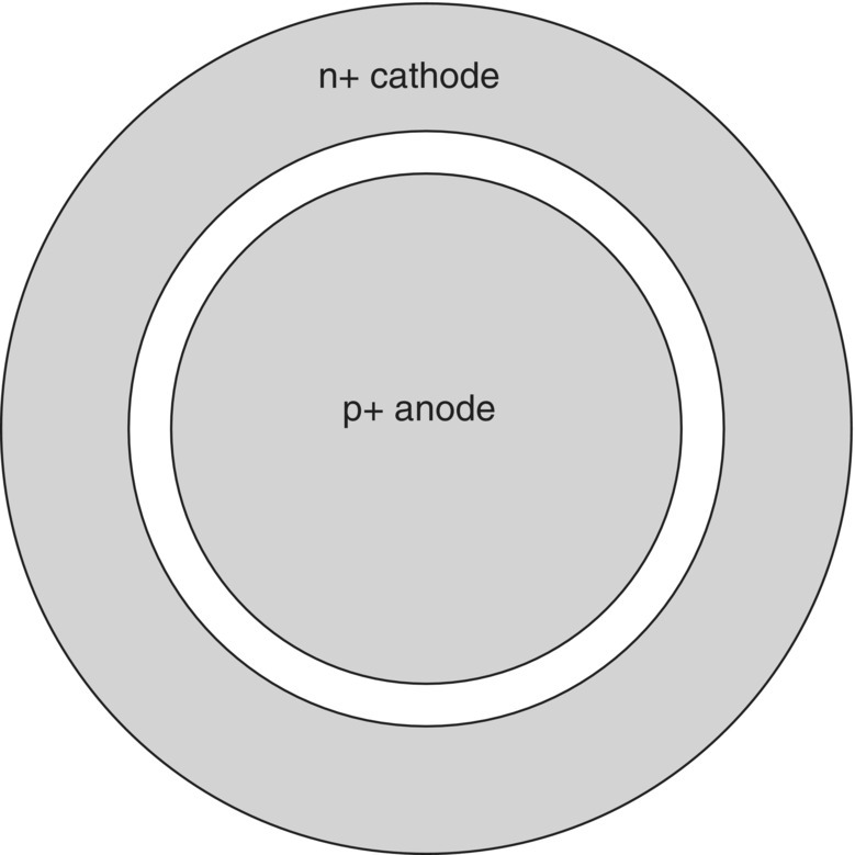
Figure 2.18 Diode layout design—circular design.
Figure 2.19 is an example of an octagonal design. Octagonal design layout is also preferred over circular layout in some design systems.
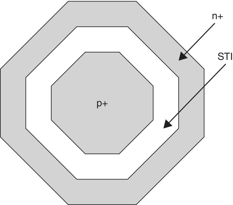
Figure 2.19 Diode layout design—octagonal design.
The disadvantages of an analog circular element are as follows [17]:
- Design width and area limitations.
- Computer-aided design (CAD) issues with nonrectangular shapes.
- CAD automation convergence and process time.
- CAD-parameterized cells for nonrectangular shapes are not always possible preventing variation in the size of the RF ESD element for different circuits or applications.
- Lithography, etch, and polishing issues.
- Limitation on the wire density.
2.10 MOSFET Design
MOSFET device layout and design is critical to both analog design and ESD. For both analog design and ESD robustness, design symmetry and matching is critical. Figure 2.20 is an example of a single-finger MOSFET layout.
Figure 2.20 Single-finger MOSFET layout.
It is an analog circuit design practice and an ESD design synthesis practice to provide a linewidth which is well controlled. For line-to-line space, in an array of lines, the spacing is maintained to provide maximum matching between adjacent lines. For example, in a multifinger MOSFET structure, the spacing between the polysilicon lines is equal to provide the maximum matched characteristics. Figure 2.21 shows an example of design symmetry for a MOSFET structure.

Figure 2.21 Symmetry MOSFET layout.
Given any array of parallel lines, the characteristics of the “end” or edges of the array can have different characteristics than the other lines. In an array of lines, whereas one edge is adjacent to another line, the other edge is not; this leads to one line-to-line edge space to appear “nested” and the outside line-to-line edge space to appear “semi-infinite” or “isolated.” To address the problem of poorly matched edge lines, the following semiconductor process and ESD design solutions are used:
- Process: Cancellation technique of photolithography and etch biases
- Design: Use of dummy edge lines
Figure 2.22 shows an example of a multifinger MOSFET layout with and without dummy lines.

Figure 2.22 Multifinger MOSFET layout with and without dummy lines.
2.11 Bipolar Transistor Design
In bipolar transistor design, bipolar transistor layout is key for both analog design and ESD [17, 19]. For both analog design and ESD robustness, design symmetry and matching is critical. Analogous to MOSFETs, similar concepts of symmetry, and common centroid, are applied with the placement of the emitter, base, and collector regions.
2.12 Closing Comments and Summary
This chapter discussed analog design layout practices of interdigitated design layout and common centroid concepts in one and two dimensions. These concepts are implemented into ESD networks and the cosynthesis of analog circuits and ESD networks.
In Chapter 3, examples of analog building blocks and circuits that exist in analog designs are provided for readers unfamiliar with analog circuit networks. The analog circuit examples include single-ended receivers, differential receivers, comparators, current mirrors, bandgap regulators, and voltage converters.
References
- 1. A. Hastings. The Art of Analog Layout. Upper Saddle River, NJ: Prentice Hall, 2006.
- 2. A.B. Glasser and G.E. Subak-Sharpe. Integrated Circuit Engineering. Reading, MA: Addison-Wesley, 1977.
- 3. A. Grebene. Bipolar and MOS Analog Integrated Circuits. New York: John Wiley & Sons, Inc., 1984.
- 4. D.J. Hamilton and W.G. Howard. Basic Integrated Circuit Engineering. New York: McGraw-Hill, 1975.
- 5. A. Alvarez. BiCMOS Technology and Applications. Norwell, MA: Kluwer Academic Publishers, 1989.
- 6. R.S. Soin, F. Maloberti, and J. Franca. Analogue-Digital ASICs, Circuit Techniques, Design Tools, and Applications. Stevenage, UK: Peter Peregrinus, 1991.
- 7. P.R. Gray and R.G. Meyer. Analysis and Design of Analog Integrated Circuits. 3rd Edition. New York: John Wiley & Sons, Inc., 1993.
- 8. F. Maloberti. Layout of analog and mixed analog-digital circuits. In: J. Franca and Y. Tsividis (Eds). Design of Analog-Digital VLSI Circuits for Telecommunication and Signal Processing. Upper Saddle River, NJ: Prentice Hall, 1994.
- 9. D.A. Johns and K. Martin. Analog Integrated Circuit Design. New York: John Wiley & Sons, Inc., 1997.
- 10. R. Geiger, P. Allen, and N. Strader. VLSI: Design Techniques for Analog and Digital Circuits. New York: McGraw-Hill, 1990.
- 11. V. Vashchenko and A. Shibkov. ESD Design for Analog Circuits. New York: Springer, 2010.
- 12. H. Kunz, G. Boselli, J. Brodsky, M. Hambardzumyan, and R. Eatmon. An automated ESD verification tool for analog design. Proceedings of the Electrical Overstress/Electrostatic Discharge (EOS/ESD) Symposium, 2010; 103–110.
- 13. S. Voldman. Electrical Overstress (EOS): Devices, Circuits, and Systems. Chichester, UK: John Wiley & Sons, Ltd, 2013.
- 14. S. Voldman. ESD Basics: From Semiconductor Manufacturing to Product Use. Chichester, UK: John Wiley & Sons, Ltd, 2012.
- 15. S. Voldman. ESD: Physics and Devices. Chichester, UK: John Wiley & Sons, Ltd, 2004.
- 16. S. Voldman. ESD: Circuits and Devices. Chichester, UK: John Wiley & Sons, Ltd, 2005.
- 17. S. Voldman. ESD: RF Circuits and Technology. Chichester, UK: John Wiley & Sons, Ltd, 2006.
- 18. S. Voldman. Latchup. Chichester, UK: John Wiley & Sons, Ltd, 2007.
- 19. S. Voldman. ESD: Failure Mechanisms and Models. Chichester, UK: John Wiley & Sons, Ltd, 2009.