
4
Analog ESD Circuits
4.1 Analog ESD Devices and Circuits
ESD protection for analog design utilizes a wide variety of ESD networks due to a broad spectrum of application spaces. In this chapter, low-voltage to high-voltage ESD devices will be discussed [1–13].
4.2 ESD Diodes
ESD diodes are used for analog design for low-voltage applications from receivers for single-ended and differential pair receivers [2–4]. Many analog applications cannot utilize these devices due to voltage tolerance issues.
4.2.1 Dual Diode and Series Diodes
A common on-chip protection network used in complementary metal-oxide semiconductor (CMOS) technology is the dual-diode (DD) network. With the introduction of the n-channel and p-channel transistor on the same wafer, a protection network using the p- and n-diffusions for diode elements is possible. Figure 4.1 contains the circuit schematic of the DD ESD network [1–4]. This network can be responsive to both electrical overstress (EOS) and ESD events [7, 8]. This network is bidirectional and symmetric turn-on.

Figure 4.1 DD ESD network.
4.2.2 Dual Diode–Resistor
A common on-chip protection network used in CMOS technology is the DD network with a series resistor. Whereas high-speed digital and radio frequency (RF) applications minimize the series resistance on receivers, analog applications can have resistors with significant resistance magnitude (Figure 4.2) [1–3].

Figure 4.2 DD–resistor ESD network.
4.2.3 Dual Diode–Resistor–Dual Diode
In CMOS technology, circuits are customized to address specific ESD events. Some of these circuits will also function to address EOS event; but others are not designed for EOS events [1–11]. Figure 4.3 is an example of a circuit to address charged device model (CDM) events. These circuits are used to establish an alternate current path so that the CDM current does not flow through small structures and gated structures. CDM circuitry diverts current from charge that was stored on the VDD power rail or the VSS substrate. These CDM circuits are typically second-stage elements placed close to the failing circuit element. These circuits are low capacitance and small and may not assist for EOS events.
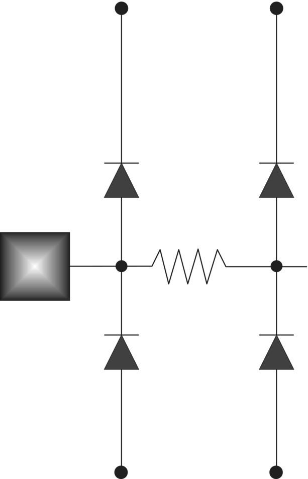
Figure 4.3 DD–resistor–DD ESD network.
4.2.4 Dual Diode–Resistor–Grounded-Gate MOSFET
These CDM circuits are typically second-stage elements placed close to the failing circuit element [1–4, 9–11]. These circuits are low capacitance and small and may not assist for EOS events. Figure 4.4 shows an ESD network consisting of a DD, a resistor, and a grounded-gate n-channel MOS (GGNMOS) device.

Figure 4.4 (a) DD–resistor ESD network (b) DD–resistor-GGNMOS ESD network.
4.2.5 Back-to-Back Diode Strings
In integration of analog and digital networks, it is a common practice to isolate the analog function from the core logic sector to reduce the noise injection from simultaneous switching noise of the digital circuitry [2–9]. Yet, complete isolation can introduce ESD failure of the analog sector when no electrical current path exists. It is not desirable to have direct electrical connections between the VDD-to-analog VDD and power rails using ESD power clamps. A preferred choice is to utilize ESD power clamps in its own power domain and to provide bidirectional connectivity through the substrate.
In digital circuit applications, the number of diode elements is chosen to allow voltage differential between the ground rails. The placement of ESD networks between ground rails influences both ESD and noise.
ESD design practices in the integration of analog and digital chip sectors are as follows:
- Utilize bidirectional element ESD networks between the ground rails of the analog and digital sectors.
- Choose the number of diodes in series based on both the necessary voltage differential and the capacitive coupling requirements.
Typical ESD protection can consist of the following ESD solutions:
- Symmetric back-to-back diode strings
- Asymmetric back-to-back diode strings
4.2.5.1 Back-to-Back Symmetric Diode String
Symmetric back-to-back diode strings are needed in designs that need design symmetric voltage margins or differential circuitry [2–9]. Figure 4.5 shows a back-to-back diode string between the two ground connections between analog and digital core domains.

Figure 4.5 Back-to-back symmetric diode string ESD network.
4.2.5.2 Back-to-Back Asymmetric Diode String
Asymmetric back-to-back diode strings can be used in designs that do not need design symmetric voltage margins Figure 4.6 shows an asymmetric back-to-back diode string between the two ground connections between an analog core and digital core.

Figure 4.6 Back-to-back asymmetric diode string ESD network.
4.3 ESD MOSFET Circuits
CMOS technology consists of two active elements—the n-channel metal-oxide semiconductor field effect transistor (MOSFET) and the p-channel MOSFET. Figure 4.7 shows an example of an n-channel MOSFET structure. An n-channel MOSFET consists of a source, drain, gate, and substrate. The source and drain are self-aligned to the MOSFET gate structure. In the n-channel MOSFET, the source and drain are n-doped. The n-channel MOSFET is placed on a p-substrate. The placement of an n-channel MOSFET on a substrate introduces a parasitic p–n diode between the substrate and the MOSFET source and drain; these parasitic diodes can become forward active during ESD and EOS events [1–11].

Figure 4.7 CMOS n-channel MOSFET.
4.3.1 Grounded-Gate MOSFET
A second common on-chip protection network used in CMOS technology is the grounded-gate n-channel MOSFET network; this is referred to as the GGNMOS protection circuit [2, 4, 7–11, 13]. In this protection network, the MOSFET gate is grounded to keep it off during positive voltage excursions. Figure 4.8 contains the circuit schematic of the GGNMOS network. This network can be responsive to both EOS and ESD events. The network turn-on occurs for positive voltage excursions above the MOSFET-gated breakdown voltage. For negative excursions, the MOSFET n-channel diffusion forward biases to the substrate. This protection is fundamentally bidirectional and asymmetric.
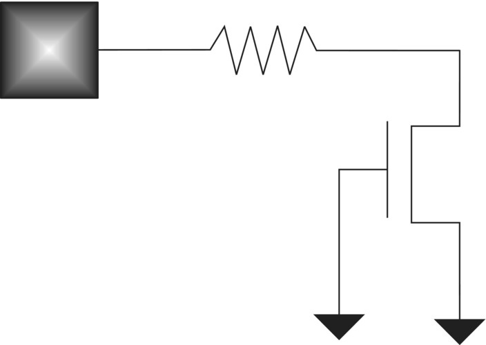
Figure 4.8 Grounded-gate NMOS (GGNMOS).
MOSFET devices undergo electrocurrent constriction at high currents. Electrocurrent constriction leads to lower high-current robustness of a MOSFET device. Ballasting techniques are introduced into MOSFET structures to provide uniform current distribution within a MOSFET “finger” as well as MOSFET current distribution finger to finger in a multifinger MOSFET structure. Figure 4.9 shows an example of a silicide block MOSFET layout that will provide a more robust MOSFET device.
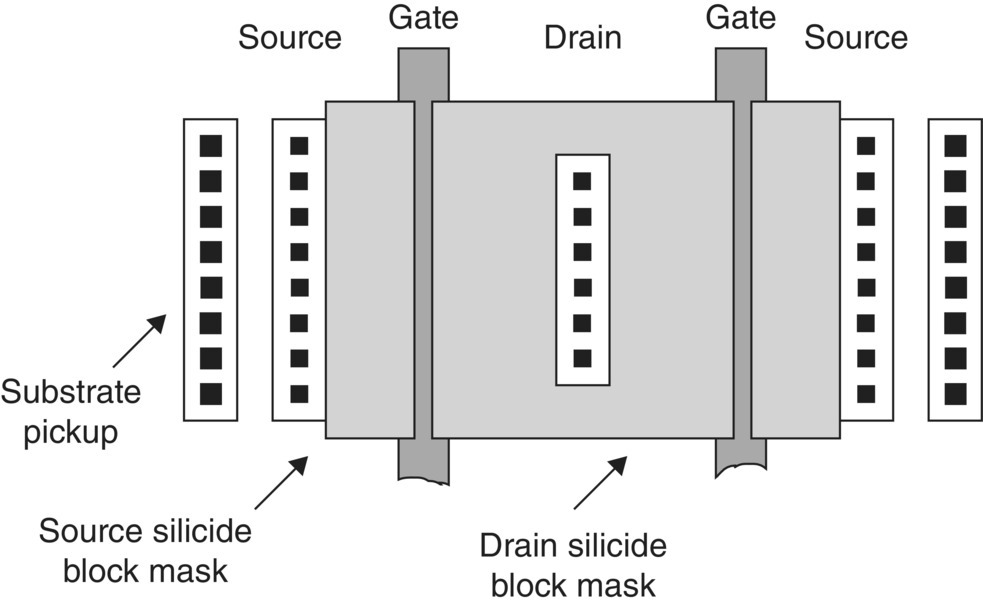
Figure 4.9 Silicide block CMOS MOSFET.
4.3.2 RC-Triggered MOSFET
For analog applications, large MOSFETs are used on signal pins and between power rails. For low-voltage CMOS (LVCMOS) applications, a commonly used ESD network between a power rail and ground rail is the RC-triggered MOSFET circuit [2–11, 13]. In analog power application, this can be used on output nodes for voltage converters and other analog circuit applications.
MOSFETs undergo electrocurrent constriction at high currents. Electrocurrent constriction leads to lower high-current robustness of a MOSFET device; in multifinger structures, nonuniform current distribution leads to the lack of scaling of the MOSFET with MOSFET width in a multifinger MOSFET. Without ballasting techniques, MOSFET current distribution finger to finger in a multifinger MOSFET structure does not always occur. By “gate-driving” the large MOSFET structure, all of the MOSFET fingers will turn on, leading to scaling of the MOSFET operation with MOSFET width.
Using a frequency trigger that responds to the HBM pulse leads to turn-on of the structure from an HBM ESD event, but does not turn on during normal chip operation (Figure 4.10).

Figure 4.10 RC-triggered CMOS MOSFET.
4.4 ESD Silicon-Controlled Rectifier Circuits
In CMOS technology, protection circuits that provide an S-type I–V characteristic can provide a voltage blocking state and a low-voltage/high-current state. Silicon-controlled rectifiers (SCR) provide an S-type I–V characteristic and are commonly used for ESD protection [2–13]. SCR provide significant ESD robustness and hence are desirable in many applications from low-voltage to high-voltage power supplies. They are suitable for electrical overcurrent (EOC) events due to their high current-carrying capabilities.
4.4.1 Unidirectional SCR
SCR are of different classifications and some are desirable for one polarity. Figure 4.11 is an example of a unidirectional SCR that provides an S-type I–V characteristic with a voltage blocking state and a low-voltage/high-current state [2–13].

Figure 4.11 Unidirectional SCR network.
4.4.2 Bidirectional SCR
Some SCR require bidirectionality due to a symmetric signal swing. Figure 4.12 is an example of a bidirectional SCR that provides an S-type I–V characteristic with a voltage blocking state and a low-voltage/high-current state in both positive and negative polarities [2–13].
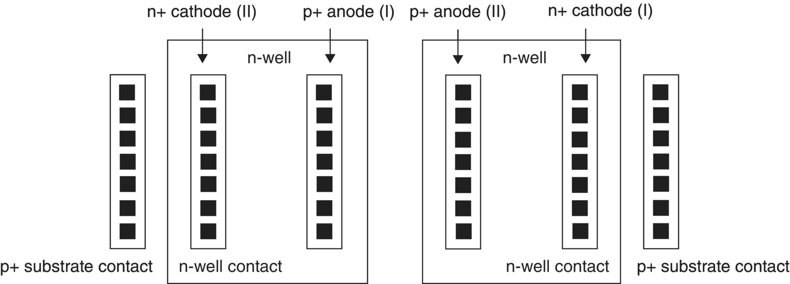
Figure 4.12 Bidirectional SCR network.
4.4.3 Medium-Level Silicon-Controlled Rectifier
In CMOS technology, protection circuits that provide an S-type I–V characteristic can provide a voltage blocking state and a low-voltage/high-current state. SCR provide an S-type I–V characteristic and are commonly used for ESD protection [11]. Figure 4.13 is an example of a CMOS technology medium-level silicon-controlled rectifier (MLSCR). An MLSCR has a high trigger voltage and so is suitable for electrical overvoltage (EOV) events [11]. The trigger voltage can exceed the power supply voltage of native CMOS technology. Additionally, it is suitable for EOC events due to their high current-carrying capabilities.

Figure 4.13 MLSCR network.
4.4.4 Low-Voltage-Triggered SCR
Figure 4.14 is an example of a CMOS technology low-voltage-triggered silicon-controlled rectifier (LVTSCR) [11]. An LVTSCR has a low trigger voltage by integrating a MOSFET into the pnpn circuit. The advantage of the LVTSCR is that it has a trigger condition closer to the native power supply voltage of the component. LVTSCR are suitable for EOC events due to their high current-carrying capabilities. As a result, these structures are suitable for improving the ESD and EOS protection levels of a component. SCR devices are inherently power devices with good EOS robustness [8].

Figure 4.14 LVTSCR network.
In the prior discussion, the devices are single direction devices or have an asymmetric response to ESD or EOS events. Bidirectional protection networks can be created that provide a symmetric voltage response.
4.5 Laterally Diffused MOS Circuits
Laterally diffused MOS (LDMOS) transistors are used for smart power technology to support higher voltages. Today, LDMOS transistors are being integrated with LVCMOS and bipolar transistors. Integration of the bipolar transistors, LVCMOS, and DMOS transistors is commonly referred to as BCD technology.
4.5.1 LOCOS-Defined LDMOS
Figures 4.15 and 4.16 show examples of the medium-voltage LDMOS (MV-LDMOS) transistor and high-voltage LDMOS (HV-LDMOS) transistors implemented in a LOCOS-isolation technology [6–8, 11, 13]. LOCOS isolation was used in base CMOS technology from 2.0 to 0.8 µm generations to define the MOSFET source and drain regions. In both transistors, the drain region is extended to reduce the surface electric field. This is also referred to as RESURF transistor. In the case of the HV-LDMOS transistor device, the MOSFET gate structure extends over the LOCOS-isolation region. The extension of the gate over the LOCOS isolation lowers the electric field in the MOSFET drain region and decreases gate modulation of the MOSFET drain structure.
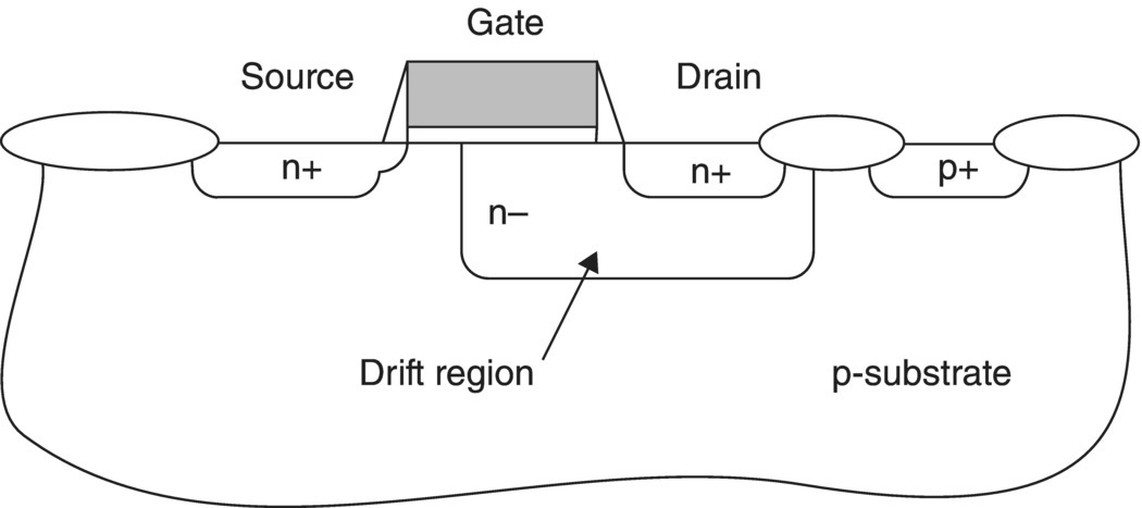
Figure 4.15 LOCOS-defined MV-LDMOS transistor structure.

Figure 4.16 LOCOS-defined HV-LDMOS transistor structure.
An advantage of LOCOS isolation is that the MOSFET junction depth is deeper than the isolation region. When the MOSFET source and drain junctions are deeper than the isolation, current can flow laterally without impediment from the isolation structure. Current crowding can be reduced near the device surface, which leads to a lower temperature internal to the semiconductor chip. A disadvantage of the LOCOS isolation is that the metallurgical junction electric field increases as the MOSFET source and drain junctions are scaled. As the junction is scaled, the radius of the metallurgical junction increases, leading to higher electric field at the junction edge; this leads to lower breakdown voltages. A second disadvantage is the MOSFET channel width control; this leads to MOSFET ΔW variation.
4.5.2 STI-Defined LDMOS
In base CMOS technology, shallow trench isolation (STI) was integrated to eliminate LOCOS-isolation bird’s beak control issues. In STI technology, the MOSFET source and drain junctions are shallower than the isolation depth. From a smart power perspective, STI reduces the lateral current and lateral heat transfer along the device surface. From electrothermal simulation, it is clear that the peak lattice temperature in STI-defined diodes increases (compared to LOCOS-defined diodes) [6–8, 11, 13]. A second concern is the sharp corners introduced in the LDMOS drift region. With technology scaling, STI-defined LDMOS transistors are needed to integrate with the STI-defined LVCMOS technology. Figures 4.17 and 4.18 are a cross section of the STI-defined MV-LDMOS and HV-LDMOS transistors, respectively.
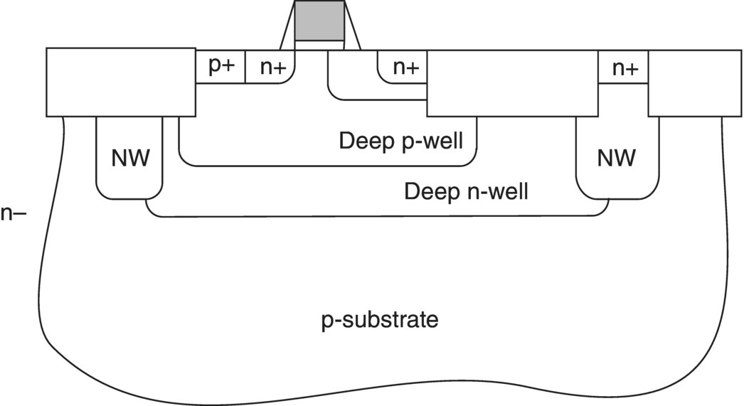
Figure 4.17 STI-defined MV-LDMOS transistor structure.

Figure 4.18 STI-defined HV-LDMOS transistor structure.
4.5.3 STI-Defined Isolated LDMOS
In LDMOS technology, the application voltages include 125, 50, and 45 V applications. In an LVCMOS STI technology, MOSFET n-type or p-type junction breakdown voltages are typically 12–18 V, and the CMOS n-well-to-substrate breakdown voltages are below 45 V. As a result, the n-channel and p-channel low-voltage technology transistors must be isolated from the substrate. In addition, the LDMOS transistors must also have metallurgical junctions which can sustain the higher-voltage applications. LDMOS technology uses deep diffused wells (instead of retrograde implanted well) with high breakdown voltages. These diffused wells can also serve to isolate the LVCMOS transistors from the substrate voltage conditions. Figures 4.19 and 4.20 are a cross section of the isolated STI-defined MV-LDMOS and HV-LDMOS transistors [6–8, 11, 13].
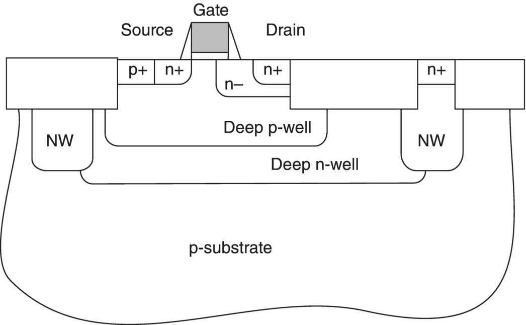
Figure 4.19 STI-defined medium-voltage isolated LDMOS transistor structure.

Figure 4.20 STI-defined high-voltage isolated LDMOS transistor structure.
Figure 4.21 is an example layout for a HV-LDMOS. For high-voltage applications, circular design layout provides avoidance of corners and provides symmetry for good current distribution. Figure 4.22 is an example of a transmission line pulse (TLP) I–V characteristic of an LDMOS transistor [6–8, 11, 13].

Figure 4.21 LDMOS circular design.

Figure 4.22 LDMOS TLP current versus voltage (I–V) characteristic.
4.6 DeMOS Circuits
High-voltage applications can utilize another type of transistor, known as the drain-extended NMOS (DeNMOS). DeNMOS transistors can also be modified to integrate a SCR within the DeNMOS transistor [7, 8, 11, 13].
4.6.1 DeNMOS
DeNMOS transistor devices introduce a drift region within the drain region to provide a voltage drop within the drain structure. Figure 4.23 shows a cross section of the DeNMOS transistor. The DeNMOS drain region can be modified by extending the distance from the DeNMOS drain contact to gate spacing.
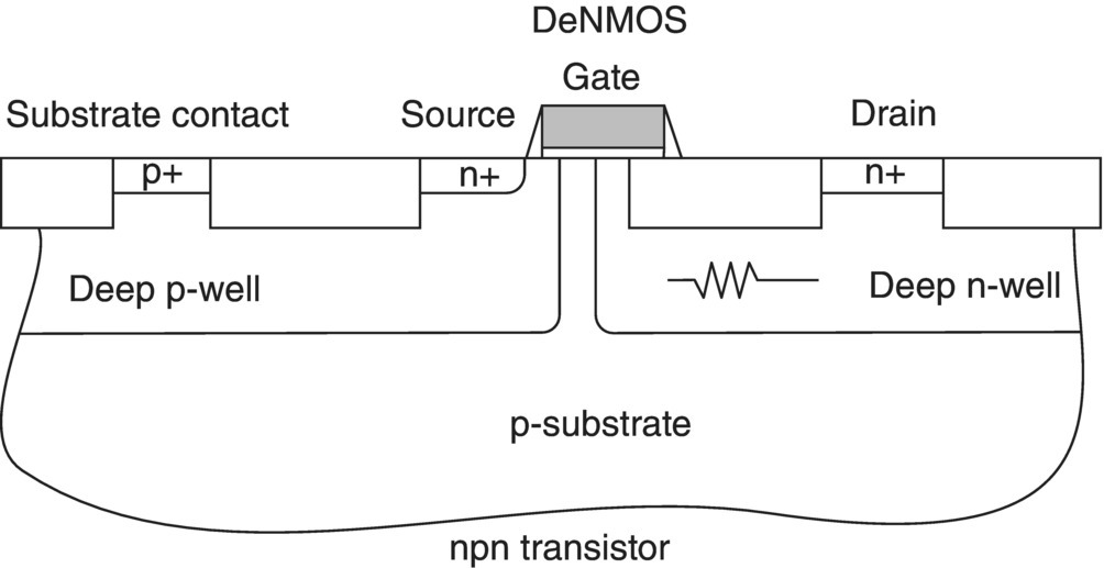
Figure 4.23 DeNMOS transistor cross section.
4.6.2 DeNMOS-SCR
DeNMOS can introduce a p-diffusion region within the drain structure. With the introduction of a p+ diffusion, a pnp can be integrated with the npn transistor to form a DeNMOS-SCR structure. Figure 4.24 shows a cross section of the DeNMOS-SCR transistor. The DeNMOS drain region can be modified by extending the distance from the DeNMOS drain contact to gate spacing. A two-transistor schematic representation is also included in Figure 4.24. In the schematic, the p-well and n-well shunt resistors are also represented. DeNMOS can be used for 40–60 V analog applications.

Figure 4.24 DeMOS-SCR transistor cross section.
4.7 Ultrahigh-Voltage LDMOS Circuits
In analog design, there are applications that require 600–700 V applied to the semiconductor chip. Ultrahigh-voltage (UHV) technology will require structures where voltages of this magnitude can be applied. In the following section, two types of UHV ESD structures are discussed [13].
4.7.1 Ultrahigh-Voltage LDMOS
For UHV applications, the semiconductor technology and layout must be modified to allow voltages over 500 V [13]. For semiconductor technology requirements, the breakdown voltages of the various metallurgical junctions must be adequate. Secondly, the device layout must allow for lateral voltage drops to allow the distribution of the voltage. Figure 4.25 shows an example layout for ultrahigh-voltage LDMOS (UHV-LDMOS) transistor. The UHV-LDMOS transistor utilizes circular geometry. Figure 4.26 shows an example layout for UHV-LDMOS transistor utilizing a “racetrack” layout.

Figure 4.25 UHV-LDMOS layout design: circular design.

Figure 4.26 UHV-LDMOS layout design: racetrack.
4.7.2 Ultrahigh-Voltage LDMOS SCR
For UHV applications, UHV-LDMOS transistors can be modified to include a p+ diffusion to form a UHV-LDMOS SCR structure [13]. Figure 4.27 shows a cross section of the UHV-LDMOS SCR structure. Figure 4.28 shows an example layout for UHV-LDMOS SCR device utilizing a “racetrack” layout.
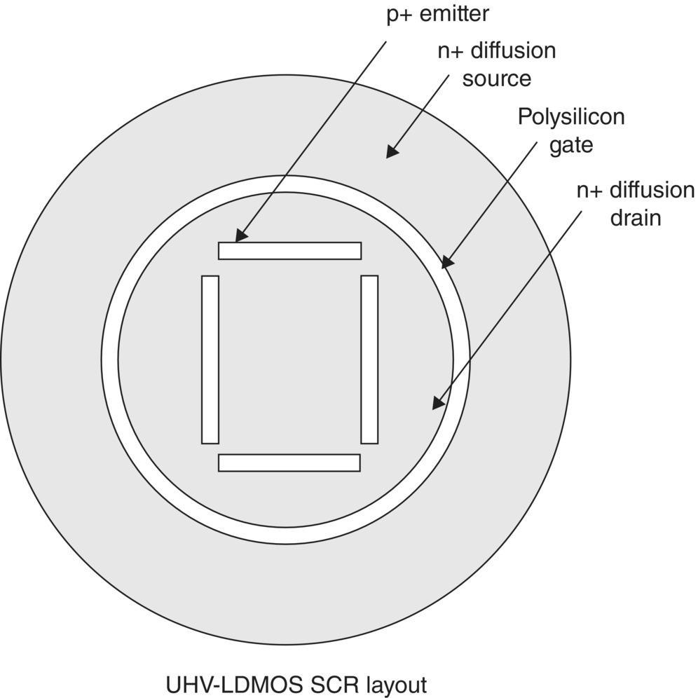
Figure 4.27 UHV-LDMOS SCR layout design: circular layout.

Figure 4.28 UHV-LDMOS SCR layout design: racetrack layout.
4.8 Closing Comments and Summary
This chapter provided examples of ESD devices used in analog semiconductor chip design. The ESD device examples include both low-voltage and high-voltage ESD networks from diodes, MOSFETs, LDMOS, and DeMOS devices in parallel and series configurations. It closed with examples of UHV devices.
In Chapter 5, semiconductor chip architecture in analog and analog-to-digital applications are discussed. Examples of analog ESD failures associated with both circuits and early design architectures are shown. Architectural changes and circuit solutions to address ESD failures are highlighted.
References
- 1. S. Voldman. ESD: Physics and Devices. Chichester, UK: John Wiley & Sons, Ltd, 2004.
- 2. S. Voldman. ESD: Circuits and Devices. Chichester, UK: John Wiley & Sons, Ltd, 2005.
- 3. S. Voldman. ESD: RF Circuits and Technology. Chichester, UK: John Wiley & Sons, Ltd, 2006.
- 4. S. Voldman. ESD: Failure Mechanisms and Models. Chichester, UK: John Wiley & Sons, Ltd, 2009.
- 5. M. Mardiquan. Electrostatic Discharge: Understand, Simulate, and Fix ESD Problems. Hoboken, NJ: John Wiley & Sons, Inc., 2009.
- 6. S. Voldman. ESD: Design and Synthesis. Chichester, UK: John Wiley & Sons, Ltd, 2011.
- 7. S. Voldman. ESD Basics: From Semiconductor Manufacturing to Product Use. Chichester, UK: John Wiley & Sons, Ltd, 2012.
- 8. S. Voldman. Electrical Overstress (EOS): Devices, Circuits and Systems. Chichester, UK: John Wiley & Sons, Ltd, 2013.
- 9. S. Dabral and T.J. Maloney. Basic ESD and I/O Design. New York: John Wiley & Sons, Ltd, 1998.
- 10. A.Z.H. Wang. On Chip ESD Protection for Integrated Circuits. New York: Kluwer Publications, 2002.
- 11. A. Amerasekera and C. Duvvury. ESD in Silicon Integrated Circuits. 2nd Edition. Chichester, UK: John Wiley & Sons, Ltd, 2002.
- 12. A. Hastings. The Art of Analog Layout. Upper Saddle River, NJ: Prentice Hall, 2006.
- 13. V. Vashchenko and A. Shibkov. ESD Design in Analog Circuits. New York: Springer, 2010.