
6
Analog-to-Digital ESD Design Synthesis
6.1 Digital and Analog
In mixed-signal chips, analog and digital functions are isolated into functional blocks to reduce noise coupling between the digital circuitry and analog functions. The switching noise of the digital circuitry must be isolated to avoid analog functional failures. Figure 6.1 shows an example of a semiconductor chip with separated digital and analog domains. Semiconductor chip architectures today provide the following solutions: (i) separate digital and analog circuit domains, (ii) separate digital and analog VDD power rails, (iii) separate digital VSS (DVSS) and analog VSS (AVSS) power rails, (iv) an ESD power clamp for each independent domain, and (v) a bidirectional symmetric diode string between DVSS and AVSS.

Figure 6.1 Digital and analog domains.
In the ESD design synthesis process, there is a flow of steps and procedures to construct a semiconductor chip. The following design synthesis procedure is an example of an ESD design flow needed for semiconductor chip implementations:
- I/O, domains, and core floor plan: Define floor plan of regions of cores, domains, and peripheral I/O circuitry.
- I/O floor plan: Define area and placement for I/O circuitry.
- ESD signal pin floor plan: Define ESD area and placement.
- ESD power clamp network floor plan: Define ESD power clamp area and placement for a given domain.
- ESD domain-to-domain network floor plan: Define ESD networks between the different chip domain area and placement for a given domain.
- ESD signal pin network definition: Define ESD network for the I/O circuitry.
- ESD power clamp network definition: Define ESD power clamp network within a power domain.
- Power bus definition and placement: Define placement, bus width, and resistance requirements for the power bus.
- Ground bus definition and placement: Define placement, bus width, and resistance requirements for the ground bus.
- I/O to ESD guard rings: Define guard rings between I/O and ESD networks.
- I/O internal guard rings: Define guard rings within the I/O circuitry.
- I/O external guard rings: Define guard rings between I/O circuitry and adjacent external circuitry.
In this chapter, the focus will be on digital-to-analog interdomain issues.
6.2 Interdomain Signal Line ESD Failures
In foundry and ASIC environments, chips are segregated into “cores” or subfunctions. Where “cores” are established, the chip is naturally segregated into separate functions, and functional blocks are assembled. In ASIC applications, “voltage islands” are also formed between chip sectors for power management. In this case, many chip sectors’ power is shut down, while a given signal path remains “active.” In these applications, the power rails are isolated into separate domains, but signal lines pass from one chip subfunction to another; the electrical connectivity between these domains exist only through the common signal paths (and the substrate wafer).
6.2.1 Digital-to-Analog Signal Line Failures
A common interdomain signal line ESD failure mechanism is signal lines between separated subfunctions [1–36]. Figure 6.2 shows the case of two functional blocks, with an inverter where one is the transmitter and the other is a receiver. The ESD networks are shown in the diagram as well. E. Worley noted that during CDM stress, the receiving inverter network can experience an electrical stress on the MOSFET gate dielectric input [14]. This is due to the resistance of the VSS ground rails, the ESD diode turn-on, and the resistances. Worley noted that the transmitter n-channel MOSFET can transfer current from the charged chip substrate to the transmitter output signal. In that case, current will flow through the signal line between the transmitter and the receiver leading to MOSFET gate dielectric failure in the MOSFET receiver gate.
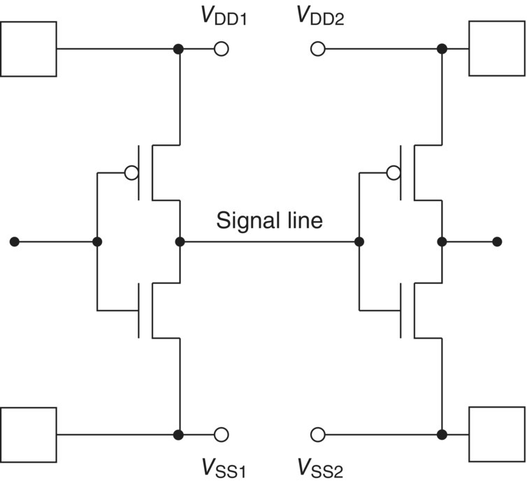
Figure 6.2 ESD interdomain failure.
A common interdomain signal line ESD failure mechanism is signal lines between digital and analog subfunctions [1–14, 34–36]. Digital-to-analog interfaces occur in digital-to-analog converters (DAC) and analog-to-digital converters (ADC). Figure 6.3 shows the case of two functional blocks, with an inverter where one is the transmitter and the other is a receiver. The ESD networks are shown in the diagram as well. As in Figure 6.2, the receiving inverter network can experience an electrical stress on the MOSFET gate dielectric input. Current will flow through the signal line between the transmitter and the receiver leading to MOSFET gate dielectric failure in the MOSFET receiver gate.
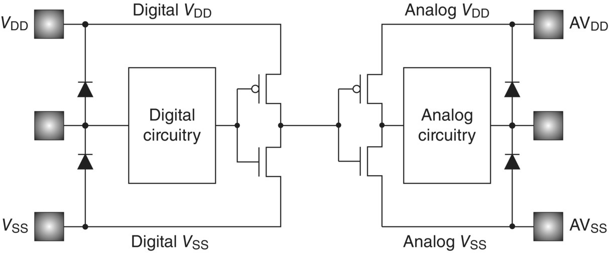
Figure 6.3 Digital-to-analog interdomain issue.
In this concept, proposed solutions to address these failure mechanisms, the following solutions were recommended:
- Resistor elements between VDD power rails (e.g., VDD to VDD) as well as VSS power rails (e.g., VSS to VSS)
- Back-to-back diodes between VDD power rails (e.g., VDD to VDD) as well as VSS power rails (e.g., VSS to VSS)
- Adding CDM ESD circuits between the transmitter and receiver networks providing an “internal” ESD network
- Adding an additional “third-party” functional block to transmit signals between a first and second functional block
- Using additional intervening blocks within the signal path
6.3 Digital-to-Analog Core Spatial Isolation
Figure 6.4 shows the floor plan of a mixed-signal semiconductor chip [34–36]. The digital and the analog cores are spatially separated. This minimizes digital noise from impacting analog circuitry.
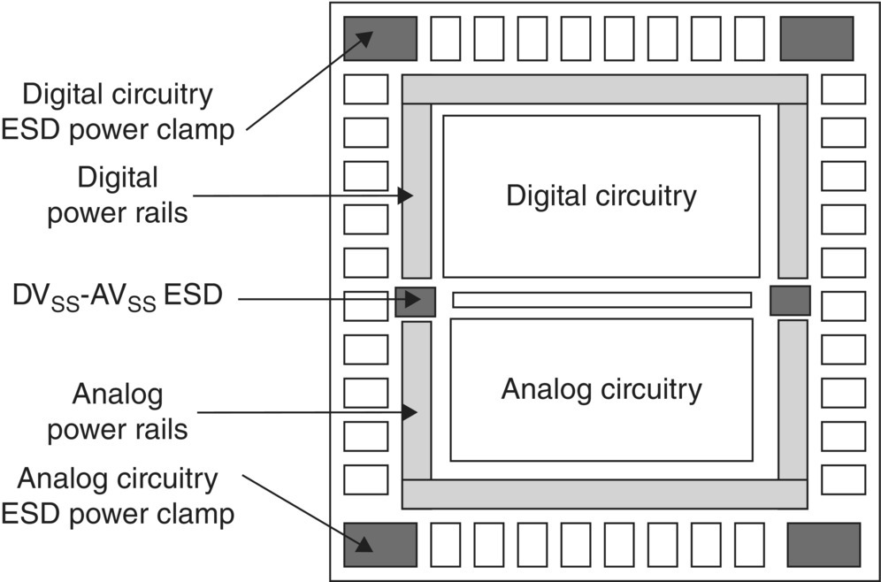
Figure 6.4 Floor plan of digital and analog domains.
6.4 Digital-to-Analog Core Ground Coupling
Figure 6.5 illustrates a circuit schematic of an ESD network between the digital and the analog grounds (e.g., DVSS to AVSS) in a mixed-signal semiconductor chip.

Figure 6.5 Circuit schematic of digital and analog domains with DVSS to AVSS.
6.4.1 Digital-to-Analog Core Resistive Ground Coupling
Figure 6.6 shows an example of an analog-to-digital domain with resistor elements between the power supplies. Resistive coupling allows for the control of the resistance between the two chip subfunctions through design.
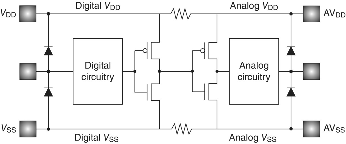
Figure 6.6 Analog-to-digital architecture with domain-to-domain resistor coupling.
6.4.2 Digital-to-Analog Core Diode Ground Coupling
Analog-to-digital subfunctions place antiparallel diode strings between the ground power rails for ESD protection [34–36]. For ESD protection, it is common to place antiparallel diode strings between the electrical grounds to establish ESD current paths between the VSS power rails (e.g., AVSS and DVSS). Figure 6.7 highlights an architecture where the VSS-to-VSS ESD power rail is an antiparallel diode string. In the placement of the antiparallel diode strings, the bus resistance of the VSS and the VDD can play a role in the voltage stress across the signal lines. In the case of signal lines between functional blocks, a voltage differential can be established between the output of a first logic block and the input of the second logic block.

Figure 6.7 ESD interdomain diode-coupling analog-to-digital solution.
6.5 Domain-to-Domain Signal Line ESD Networks
Figure 6.8 shows an example of an interdomain ESD network. For CDM solutions, the second-stage network consists of a resistor and dual-diode element [14]. Other CDM networks can consist of a resistor and MOSFET element.
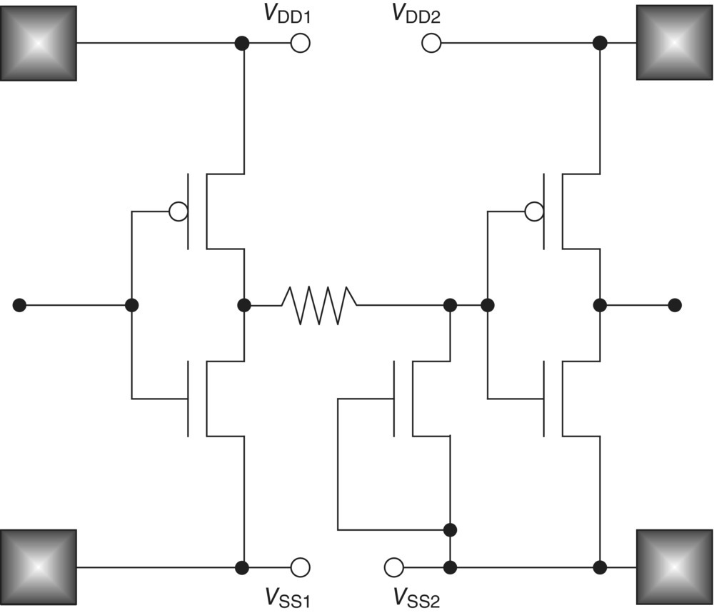
Figure 6.8 ESD interdomain CDM failure using resistor and grounded-gate NMOS (GGNMOS) circuit.
6.6 Domain-to-Domain Third-Party Coupling Networks
Voltage drops along cross-domain signal lines can be achieved by introduction of additional circuitry along the signal path. A “third-party” functional block to transmit the signals between the transmitter and the receiver can be introduced [14]. This third-party block contains two inverters in series, supportive ESD elements, and its own independent power rails (Figure 6.9).

Figure 6.9 ESD interdomain third-party functional block circuit.
6.7 Domain-to-Domain Cross-Domain ESD Power Clamp
A means to avoid current flow from the digital power rail (DVDD) and the analog ground rail (AVSS) can be achieved by introduction of a “cross-domain” ESD network [34–36]. Figure 6.10 illustrates a circuit schematic highlighting the cross-domain ESD network. The cross-domain ESD network can be the following:

Figure 6.10 ESD cross-domain power clamp.
- Silicon-controlled rectifier (SCR)
- GGNMOS
- Series diodes
- RC-triggered MOSFET power clamp
6.8 Digital-to-Analog Domain Moat
In mixed-signal applications, noise isolation and substrate injection are critical for analog circuitry. Noise isolation can be improved by placement of a “moat” that isolated the digital and analog core regions (Figure 6.11) [34–36]. With the placement of a “moat,” the resistance between the two regions can be increased to provide improved noise isolation. Additionally, the minority carrier transport between the digital and analog domains can be decreased.
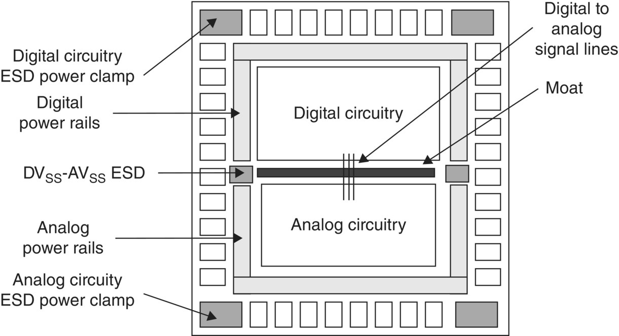
Figure 6.11 Digital-to-analog moat.
6.9 Digital-to-Analog Domain Moat with Through-Silicon Via
In system-on-chip (SOC), 2.5-D, and 3-D applications, through-silicon via (TSV) structures are integrated into the technology. TSV structures are integrated into memory, microprocessors, and other mixed-signal applications. Noise isolation can be improved by placement of the TSV structures within the moat that isolated the digital and analog core regions (Figure 6.12). With the placement of an array of TSV structures or “bar” TSV structures (e.g., high aspect ratio length and width), the resistance between the two regions can be increased to provide improved noise isolation [37–45]. Additionally, the minority carrier transport between the digital and analog domains can be decreased.

Figure 6.12 Digital-to-analog floor plan with TSV within the moat region.
6.10 Domain-to-Domain ESD Design Rule Check and Verification Methods
ESD checking and verification are used to address finding the cross-domain signal lines to avoid ESD failure [15–33]. These ESD design checking used various methods that address circuit topology connectivity and resistance along the signal lines that cross the digital-to-analog domain. This will be discussed in Chapter 12.
6.11 Closing Comments and Summary
This chapter addressed integration of digital and analog domains where they are required to be decoupled due to noise. Electrical isolation of the two domains leads to ESD failures between the grounds, as well as along signal lines that cross these separated domains. ESD solutions between the ground connections include coupling using resistors and diode elements, as well as third-party functional blocks. ESD solutions along the signal lines include the ground connections as well as the ESD networks on the signal lines that cross the digital-to-analog domain.
Chapter 7 addresses analog and ESD signal pin cosynthesis that introduces usage of interdigitated layout and common centroid concepts to provide ideal matching, low capacitance, and small area in differential signal pins. Using interdigitated designs, the parasitic elements are utilized for signal pin-to-signal pin ESD protection.
References
- 1. C. Johnson, T.J. Maloney, and S. Qawami. Two unusual HBM ESD failure mechanisms on a mature CMOS process. Proceedings of the Electrical Overstress/Electrostatic Discharge (EOS/ESD) Symposium, 1993; 225–231.
- 2. H. Terletzki, W. Nikutta, and W. Reczek. Influence of the series resistance of on-chip power supply buses on internal device failure after ESD stress. IEEE Transactions on Electron Devices, ED-40(11), November 1993; 2081–2083.
- 3. M.D. Ker, C.Y. Wu, T. Cheng, C.N. Wu, T.L. Yu, and A.C. Wang. Whole chip ESD protection for VLSI/ULSI with multiple power pins. Proceedings of the International Reliability Workshop (IRW), 1994; 124–128.
- 4. W. Reczek and H. Terletzski. Integrated semiconductor circuit with ESD protection. U.S. Patent No. 5,426,323, June 20, 1995.
- 5. M.D. Ker and T.L. Yu. ESD protection to overcome internal gate-oxide damage on digital-analog interface of mixed-mode CMOS IC’s. Microelectronics Reliability, 36(11/12), 1996; 1727–1730.
- 6. I. Chyrsostomides, X. Guggenmos, W. Nikkuta, W. Reczek, J. Rieger, J. Stecker, and H. Terletzski. Semiconductor component with protective structure for protecting against electrostatic discharge. U.S. Patent No. 5,646,434, July 8, 1997.
- 7. H. Imamura. Semiconductor device having individual power supply lines shared between function blocks for discharging surge without propagation of noise. European Patent Application 97108486.8, March 12, 1997.
- 8. M.D. Ker, C.Y. Wu, H.H. Chang, and T.S. Wu. Whole chip ESD protection scheme for CMOS mixed-mode IC’s in deep submicron CMOS technology. Proceedings of the Custom Integrated Circuits Conference (CICC), May 5–8, 1997; 31–38.
- 9. H. Nguyen and J.D. Walker. Electrostatic discharge protection system for mixed voltage application specific integrated circuit design. U.S. Patent No. 5,616,943, April 1, 1997.
- 10. E. Worley, C.T. Nguyen, R.A. Kjar, and M. Tennyson. Method and apparatus for coupling multiple independent on-chip VDD busses to an ESD core clamp. U.S. Patent No. 5,654,862, August 5, 1997.
- 11. W. Nikkuta and W. Reczek. Integrated semiconductor circuit. U.S. Patent No. 5,821,804, October 13, 1998.
- 12. P. Minogue. ESD protection scheme. U.S. Patent No. 5,731,940, March 24, 1998.
- 13. M.D. Ker. ESD protection circuit for mixed mode integrated circuits with separated power pins. U.S. Patent No. 6,075,686, June 13, 2000.
- 14. E.R. Worley. Distributed gate ESD network architecture for inter-power domain signals. Proceedings of the Electrical Overstress/Electrostatic Discharge (EOS/ESD) Symposium, 2004; 238–247.
- 15. C. Robertson. Calibre PERC: Preventing electrical overstress failures. EE Times Design, EE Times, February 9, 2012.
- 16. TSMC Open Innovation Platform Ecosystem Forum. Improving analog/mixed signal circuit reliability at advanced nodes. EDA Technical Presentations, 2011.
- 17. M. Khazhinsky. ESD electronic design automation checks. In Compliance Magazine, August 2012.
- 18. M. Hogan. Electronic design automation checks, Part II: Implementing ESD EDA checks in commercial tools. In Compliance Magazine, September 2012.
- 19. S. Sinha, H. Swaminathan, G. Kadamati, and C. Duvvury. An automated tool for detecting ESD design errors. Proceedings of the Electrical Overstress/Electrostatic Discharge (EOS/ESD) Symposium, 1998; 208–217.
- 20. M. Baird and R. Ida. Verify ESD: A tool for efficient circuit level ESD simulations of mixed signal ICs. Proceedings of the Electrical Overstress/Electrostatic Discharge (EOS/ESD) Symposium, 2000; 465–469.
- 21. P. Ngan, R. Gramacy, C.K. Wong, D. Oliver, and T. Smedes. Automatic layout based verification of electrostatic discharge paths. Proceedings of the Electrical Overstress/Electrostatic Discharge (EOS/ESD) Symposium, 2001; 96–101.
- 22. R. Zhan, H. Xie, H. Feng, and A. Wang. ESDZapper: A new layout-level verification tool for finding critical discharging path under ESD stress. Proceedings of the ASPDAC, 2005; 79–82.
- 23. H.Y. Liu, C.W. Lin, S.J. Chou, W.T. Tu, C.H. Liu, Y.W. Chang, and S.Y. Kuo. Current path analysis for electrostatic discharge protection. Proceedings of the ICCAD, 2006; 510–515.
- 24. J. Connor, S. Mitra, G. Wiedemeir, A. Wagstaff, R. Gauthier, M. Muhammad, and J. Never. ESD simulation using fully extracted netlist to validate ESD design improvement. Proceedings of the International ESD Workshop (IEW), 2007; 396–407.
- 25. T. Smedes, N. Trivedi, J. Fleurimont, A.J. Huitsing, P.C. de Jong, W. Scheucher, and J. van Zwol. A DRC-based check tool for ESD layout verification. Proceedings of the Electrical Overstress/Electrostatic Discharge (EOS/ESD) Symposium, 2009; 292–300.
- 26. Z.Y. Lu and D.A. Bell. Hierarchical verification of chip-level ESD design rules. Proceedings of the Electrical Overstress/Electrostatic Discharge (EOS/ESD) Symposium, 2010; 97–102.
- 27. H. Kunz, G. Boselli, J. Brodsky, M. Hambardzumyan, R. Eatmon. An automated ESD verification tool for analog design. Proceedings of the Electrical Overstress/Electrostatic Discharge (EOS/ESD) Symposium, 2010; 103–110.
- 28. M. Okushima, T. Kitayama, S. Kobayashi, T. Kato, and M. Hirata. Cross domain protection analysis and verification using whole chip ESD simulation. Proceedings of the Electrical Overstress/Electrostatic Discharge (EOS/ESD) Symposium, 2010; 119–125.
- 29. M. Muhammad, R. Gauthier, J. Li, A. Ginawi, J. Montstream, S. Mitra, K. Chatty, A. Joshi, K. Henderson, N. Palmer, and B. Hulse. An ESD design automation framework and tool flow for nano-scale CMOS technology. Proceedings of the Electrical Overstress/Electrostatic Discharge (EOS/ESD) Symposium, 2010; 91–96.
- 30. G.C. Tian, Y.P. Xiao, D. Connerney, T.H. Kang, A. Young, and Q. Liu. A predictive full chip dynamic ESD simulation and analysis tool for analog and mixed signal ICs. Proceedings of the Electrical Overstress/Electrostatic Discharge (EOS/ESD) Symposium, 2011; 285–293.
- 31. N. Chang, Y.L. Liao, Y.S. Li, P. Johari, and A. Sarkar. Efficient multi-domain ESD analysis and verification for large SOC designs. Proceedings of the Electrical Overstress/Electrostatic Discharge (EOS/ESD) Symposium, 2011; 300–306.
- 32. N. Trivedi, H. Gossner, H. Dhakad, B. Stein, and J. Schneider. An automated approach for verification of on-chip interconnect resistance for electrostatic discharge paths. Proceedings of the Electrical Overstress/Electrostatic Discharge (EOS/ESD) Symposium, 2011; 307–314.
- 33. H. Marquardt, H. Wagieh, E. Weidner, K. Domanski, and A. Ille. Topology-aware ESD checking: A new approach to ESD protection. Proceedings of the Electrical Overstress/Electrostatic Discharge (EOS/ESD) Symposium, 2012; 85–90.
- 34. S. Voldman. Electrical Overstress (EOS): Devices, Circuits, and Systems. Chichester, UK: John Wiley & Sons, Ltd, 2013.
- 35. S. Voldman. ESD Basics: From Semiconductor Manufacturing to Product Use. Chichester, UK: John Wiley & Sons, Ltd, 2012.
- 36. S. Voldman. ESD: Design and Synthesis. Chichester, UK: John Wiley & Sons, Ltd, 2011.
- 37. S. Voldman. Structure and method for latchup improvement using wafer via latchup guard ring. U.S. Patent No. 7,989,282, August 2, 2011.
- 38. S. Voldman. Structure and method for latchup improvement using wafer via latchup guard ring. U.S. Patent No. 8,390,074, March 5, 2013.
- 39. P. Chapman, D.S. Collins, and S. Voldman. Structure and method for latchup robustness with placement of through wafer via within CMOS circuitry. U.S. Patent No. 8,420,518, April 16, 2013.
- 40. S. Voldman. ESD network circuit with a through wafer via structure and a method of manufacture. U.S. Patent No. 8,232,625, July 31, 2012.
- 41. P. Chapman, D.S. Collins, and S. Voldman. Structure and method for latchup robustness with placement of through wafer via within CMOS circuitry. U.S. Patent No. 8,017,471, September 13, 2011.
- 42. P. Chapman, D.S. Collins, and S. Voldman. Structure for a latchup robust array I/O using through wafer via. U.S. Patent No. 7,855,420, December 21, 2010.
- 43. P. Chapman, D.S. Collins, and S. Voldman. Latchup robust array I/O using through wafer via. U.S. Patent No. 7,741,681, June 22, 2010.
- 44. P. Chapman, D.S. Collins, and S. Voldman. Structure for a latchup robust gate array using through wafer via. U.S. Patent No. 7,696,541, April 13, 2010.
- 45. P. Chapman, D.S. Collins, and S. Voldman. Latchup robust gate array using through wafer via. U.S. Patent No. 7,498,622, March 3, 2009.