
Thunder is good, thunder is impressive; but it is the lightning that does the work.
Mark Twain
CONTENTS
10.2.1 Arcing Time in an AC Circuit
10.2.2 Arcing Time in a DC Circuit
10.2.3 Activation of the Contact
10.2.4 Arcing Time in Very Low-Current DC Circuits: Showering Arcs
10.3 Arc Erosion of Electrical Contacts
10.3.1 Erosion on Make and Erosion on Break
10.3.2 The Effect of Arc Current
10.3.3 The Effect of Contact Size
10.3.4 Determination of Contact Size in AC Operation
10.3.5 Erosion of Contacts in Low-Current DC Circuits
10.3.6 Erosion of Contacts in Low-Current AC Circuits
10.5.1 Welding of Closed Contacts
10.5.2 Welding During Contact Closure
10.5.3 Welding as Contacts Open
10.6 Changes in the Contact Surface as a Result of Arcing
10.6.2 Silver–Refractory Metal Contacts
Slepian once said if Nature had not given us an arc, then we would have had to invent one. The electric arc allows a smooth transition of the circuit current to current zero. If the current were to suddenly chop to zero once the contacts had parted, then the energy stored in the circuit inductance, L, would result in large overvoltages given by
(10.1) |
Switch designers would have to design for these voltages. Fortunately, for the most part, the presence of the arc usually limits the values of voltage to a maximum of up to two times the circuit voltage.
The consequences of this arc, however, affect all of our choices for the application of contact material. This chapter describes the effects of arcing on electrical contacts; Chapters 11 through 15 will discuss design considerations for switching devices that produce arcs as they close and open, and Chapters 16 through 19 will further discuss the consequences of arcing on electrical contacts.
10.2.1 Arcing Time in an AC Circuit
When switching normal load current, most switching devices have a maximum arcing time, th, of one half-cycle of current. Thus, for a 60-Hz circuit, the maximum arcing time is 8.3 ms and for a 50-Hz circuit, it is 10 ms. There could be the occasional operation when the contacts open just before a current zero and the arc will persist until the following current zero. If the contacts open at random then the average arcing time tb over the life of the switch will be
(10.2) |
For contacts used in devices that switch large overload currents or short-circuit currents where asymmetrical values will occur [1,2,3], the arcing time can be longer than one cycle. If, however, the arcing time is more than 23 ms for a 50-Hz circuit or 19 ms for a 60-Hz circuit (i.e., a little more than one whole cycle of current), there is usually something wrong with the design and operation of the switch.
10.2.2 Arcing Time in a DC Circuit
The duration of the arc in a DC circuit is much more complex. As the arc voltage, UA, increases to the circuit voltage, UC, the circuit current decreases to a value at which the arc can no longer be sustained. As we have seen in Section 9.7.2, at this value, the arc extinguishes and the circuit current is interrupted. However, even if UA > UC for an infinitesimally small instant of time, a finite time period is required to dissipate the ½LI2 energy stored in the circuit inductance. If we consider the circuit shown in Figure 10.1, then
(10.3) |
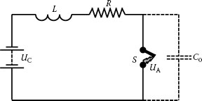
FIGURE 10.1
The direct current (DC) circuit.
where R is the circuit resistance. In principle, the exact function of time for UA can be substituted in Equation 10.3 and I as a function of time can be calculated. If the voltage of the arc formed after the rupture of the molten metal bridge is constant, Equation 10.3 can easily be solved. This case always occurs in a low-voltage DC circuit where UC is less than the minimum arcing voltage Umin, that is, where UC is less than about 12 V. A single operation of the contacts follows this sequence [4]:
1. The contacts close allowing current to flow and discharging the local contact capacitance, C0. If an arc discharge occurs at all, it will be of extremely short duration assuming there is no contact bounce.
2. The current builds up to its final value I0 = UC/R with a time constant L/R.
3. When the contacts begin to separate, the molten metal bridge is formed. As they continue to separate, the voltage across the contacts reaches the rupture voltage of the bridge, Ub. The current is now Ib=I0{1−Ub/Uc}. The time to reach the rupture voltage depends upon I0 and the opening velocity of the contacts (see Section 9.4.2).
4. The bridge ruptures and creates a region of high pressure and low conductance metal vapor between the contacts. The voltage across the contacts begins to rise at a rate which is dU/dt~Ib/C0. The value of dU/dt depends upon C0 which, in turn, depends not only upon the contact material, but also the length and diameter of the molten metal bridge, that is, upon I0. Figure 9.20 shows that for Au contacts with I0 = 20 A, dU/dt≈2.8×107 Vs−1, for Cu contacts with I0 = 150 A, dU/dt≈2.5×107 Vs−1, and for Ni contacts with I0 = 1,000 A, dU/dt≈107 Vs−1,
5. The voltage rises to a value of a few tens of volts and then drops to a value close to the minimum arc voltage associated with the contact material, Umin. (see Section 9.5.4).
6. When the gap voltage reaches Umin, an arc is initiated in the metal vapor left after the rupture of the bridge.
7. For a short arc, the arc voltage UA remains constant, and the supply voltage UC is effectively opposed by a back voltage UA. The circuit current I, thus decreases, and it is given by [4]
(10.4) |
8. The arc will continue until the current has fallen to the minimum arcing current Imin; if we substitute U0=IminR,then the arcing time ta is given by
(10.5) |
In order to simplify this, we can usually assume Im ≈ 0.
(10.6) |
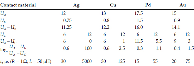
Figure 10.2 shows the arc duration, ta for gold contacts in a 6-V circuit for various values of L [5]. In Figure 10.3, ta is plotted against LI for currents ranging from 1 A to 15 A. It can be seen from Equation 10.6 that, even though the loge term does not change rapidly as (UA−UC)→0,ta will increase considerably; this is illustrated in Table 10.1. Thus, in DC circuits where the voltage can vary such as in the nominally 14-V automotive electrical circuits, it is important to design the switching system so that the UA is greater than the maximum possible value of UC. This will necessitate choosing a material with the correct Umin, as shown in Table 9.9, and/or stretching the arc to drive UA > Umin, because UA will increase both from an increase in length as well as from the substitution of O2 and N2 for metal vapor as the arcing medium (see Section 10.3.5).
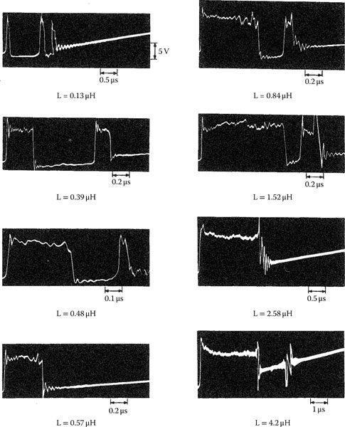
FIGURE 10.2
Arc duration for gold contacts interrupting a 6 V, 10 A, DC circuit [5].
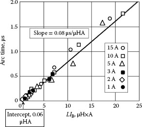
FIGURE 10.3
Arc duration as a function of circuit inductance × current for gold contacts a 6-VDC circuit [5].
TABLE 10.1
Arc Duration and the Effect of the Circuit Voltage for Low-Voltage DC Circuits
For higher voltages (say Uc in the range 100–1,000 V) the design of the switch again must ensure the development of a high UA→(UC−RI). This usually cannot be achieved by just opening the contacts further. In order to achieve a higher UA, the arc must be cooled or split into a degree of activation it into deion plates [6] or into narrow insulating slots (see Section 14.1.1). The designer has to be careful, however, not to increase UA too rapidly, because it is still possible for the arc to re-strike in the residual hot gas remaining between the contacts [7]. This will be discussed again in Section 10.3.5. For circuit voltages greater than ~1,000 V, other means have to be used to drive the current in the switch to zero. These are beyond the scope of this book, but examples of successful very high-voltage DC switches are given in [8,9].
10.2.3 Activation of the Contact
Contact activation will be introduced here and a more detailed discussion of this phenomenon will be presented in Chapter 19 (Section 19.2). The term contact activation was first used by Germer et al. [10] as “the process of particle formation on DC relay contacts that gives an increase in the duration of the relay make and break arcs.” The pioneering research by Germer and his colleagues showed this activation was the result of the deposit of carbonaceous particles. These particles are generated from organic materials that decompose under the conditions of high temperature that occur in the arc and at the contact surfaces. Visual examination of activated contacts shows that the normal, clean metallic contacts become covered with a blackish powder. SEM analysis of this black deposit shows it to be small submicron carbon particles that sometimes cluster together giving a cauliflower appearance. I suspect that Germer et al. was observing what are now called “Buckyballs” or Fullerenes [11], but in 1957, his instrumentation was not powerful enough to resolve them.
The organic vapors that produce contact activation can come from many sources. External sources—those not associated with the relay—include paint fumes, floor polish fumes, exhaust fumes, and some so-called contact cleaners. After-shave lotions and hair sprays have also been able to cause activation in the laboratory. Nature can contribute to the problem with, for example, pine vapor from pine trees. Internal sources—those associated with the relay—include plasticizers in the cellulose acetate of the coil winding, phenol from the relay structure and printed wiring boards, and organic lubricants used in conjunction with connector contacts. For relays operating in an automobile environment, the source of organic vapors is enhanced by the lubricating oils and fuel that are required to allow the automobile to function.
For relays operating in an organic ambient, it has been shown the total exposure of the contacts to organics is critical, that is the arc duration as the contacts open multiplied by the organic concentration in the ambient atmosphere is the important factor in determining the degree of activation [12]. In Figure 10.4, arc duration in microseconds is plotted as a function of the contact exposure in pascal seconds (1 pascal (Pa) = 10−2 mbar = 10−5 atmosphere at STP). Three regions are defined from the activation curve. The first is the region of limited ion drift at low exposure values, where the arc durations are independent of exposure and give values of arc duration similar to the clean activated contact. In this example, for a DC circuit of 0.5 A and 50 V, it is about 1.5 μs. The second is the region of limited diffusion at intermediate values where the durations are proportional to the square root of the exposure. Finally, there is the region of adsorption sites at high exposure values where, once again, arc durations are independent of exposure. The actual critical exposure values between the regions depend upon the organic activant and the metal being examined. A model of contact activation [12] predicts the form of the curve in Figure 10.4. From a practical point of view, the diffusion-site-limited and adsorption-site-limited regions are the most damaging, because the activation results in increased arcing time: in the example shown here, this is by a multiple of 10.
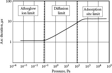
FIGURE 10.4
Note: Arc duration for activated contacts as a function of contact exposure to organic vapor [12].
A unique activation curve occurs for each metal–organic pair. Predicting how any particular combination will behave, therefore, is very difficult. However, by examining the performance of a number of metals in a number of activants, Gray et al. [12] showed that comparisons can be made. Metals examined are Au, Ag, Pd, Re, Pd–Ag and Pd–Ni, and organics used are benzene, fluorinated hydrocarbons, n-hexane, isopropanol, phenol, cyclohexane, and diethylphthalate. Rankings in terms of arc duration are shown in Table 10.2 [13]. Of the metals studied for telephone switching applications, Pd–Ni and Au appear to be the most and least resistant to activation respectively. Differentiating between organics is much more difficult; however, Gray showed that the lower critical exposure point depended upon the number of carbon atoms per molecule of the activating organic. The larger the organic molecule, in terms of the number of carbon atoms, the lower the exposure required to activate the contacts. The smaller number of organic molecules is compensated by the larger number of carbon atoms in the molecule. This is as would be expected, because the amount of carbon on the contact surfaces determines the arcing duration. The sticking coefficient of the organics on the metal surface also plays a role, as does the effect of oxygen content of the molecule [14]. Some organic lubricants, which contain a large number of carbon atoms, have been observed to cause activation at concentrations of only a few parts per trillion! Thus, while helping one system to operate, lubricant vapors can be detrimental to other nearby systems with open contacts. It has been shown, however, the electric arc is required to activate contact surfaces. Exposure to organic vapors without arcing will not result in activation [15].
TABLE 10.2
Statistical Ranking of Metals and Organic Activants on Relay Contacts
|
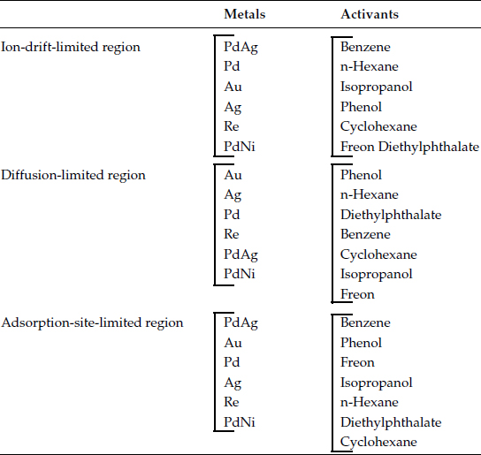
Note: The bracket indicates that statistically no difference could be detected between members of a group. Metals and activants are listed in order of decreasing arc duration.
10.2.4 Arcing Time in Very Low-Current DC Circuits: Showering Arcs
There are DC circuits where the currents are closer to or below the minimum arc current Imin (see Section 9.5.4), for example, in the range ~1 mA to ~100 mA. These circuits can still form a series of transient arcs and at currents <60 mA, transient glow discharges (see Section 9.3.3) that can affect the performance and life of the electrical contact. This discharge is called a showering arc and is described in detail by Wagar [16,17] and Miyajoma et al. [18]. A typical circuit is shown in Figure 10.5. Once the contacts open, the DC current between the contacts chops to zero if its value is low enough. The circuit’s inductance, however, will not allow the circuit’s energy to instantaneously drop to zero. The result is a transient charging and discharging of the circuit capacitance, both lumped and that distributed in the wiring. The initial rate of rise of voltage is again given by I0/C; examples are presented in Table 10.3 [16,17].
The peak voltage Up is a complex function of the circuit load, inductive energy and capacitive energy stored in the circuit [16,17]. A typical transient is shown in Figure 10.6. In Section 9.3, it has been shown if the voltage exceeds the breakdown voltage of the contact gap, then a discharge can be initiated in fractions of a microsecond. Whether or not breakdown occurs can be determined by matching the contact’s breakdown characteristic with the available circuit voltage. If we take the short gap and gas breakdown characteristics illustrated in Figures 9.12 and 9.13 and superimpose typical circuit voltage characteristics, it can be seen in Figure 10.7 that it is possible for the circuit voltage curves to exceed the voltage required to initiate a discharge. If the circuit current exceeds Imin, a sustained arc will occur between the contacts as has been discussed in Section 9.3. If the circuit current is lesser than Imin, then Figure 10.7 illustrates what can happen. If the total capacitance produces a dV/dt across the contacts of ~ 3.5 × 10⁸ V s−1, the minimum gas breakdown (350 V) is reached in ~ 1 μs. The contact spacing at this time may be a few micrometers for a typical contact. Remember this process can only begin after the rupture of the molten metal bridge. Breakdown occurs with the transient current being sufficiently high for the discharge to progress from a glow to an arc. For example, if the circuit impedance Z is ~100 Ω and the circuit voltage is 12 V, then the initial peak current at breakdown, Ip is
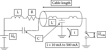
FIGURE 10.5
Low-current DC circuit [16,17].
TABLE 10.3
Typical I0/C0 Values for Low-Current Switches
I0/C0(Vs−1) |
Value of C(F) |
Possible value of I(A) |
1011 (high) |
10−10 (2 m of cable) |
10 |
2 × 10⁸ (typical) |
10−9 (20 m of cable) |
0.2 |
5 × 10⁴ (low) |
10−6 (large protection network) |
0.05 |
Activation makes contact surfaces more cathodic.
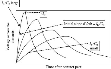
FIGURE 10.6
Voltage transient generated across the open contacts on interrupting current in a low-current DC circuit [16,17].
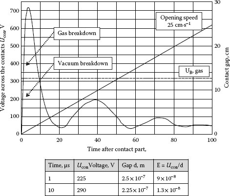
FIGURE 10.7
Breakdown as a result of the voltage transient developed across the open contacts in a low-current DC circuit [16,17].
(10.7) |
The stored energy is transferred in ~10−9 s. The breakdown surge travels from the contact to the load, which appears as a high impedance, reflecting it back towards the contact in reverse polarity. Upon arrival at the contact after a time
(10.8) |
this reverse voltage extinguishes the arc and starts a new cycle of charging in the positive direction, as before. If the reverse voltage is high enough, an arc may even form in the reverse direction. A succession of very short duration discharges occurs and it is clear why this has been termed a showering arc. It continues until the energy stored in the circuit is dissipated or until the opening contact gap causes the transient circuit voltage to fall below UB (see Figure 10.8).
This qualitative description of the showering arc was modeled by Mills [19]. One of his results is shown in Figure 10.9 and it shows a remarkable correspondence to the measured voltage transients. Miyajima et al., who used a high inductance 3.3 mA, 10 V circuit, show that the showering arc produces so much contact erosion as to change the roughness of the contact surfaces over a large number of operations. From one to 105 operations, the roughness does not change appreciably, but from 105 to 107 operations the surface roughness doubles [18]. For the very low current in their experiments the molten metal bridge that forms as the contacts open is about 0.3 μm when it ruptures; see Figure 9.18. It is, thus, possible that metal from this rupture will again bridge the contact gap and the showering arc will be delayed; see Figure 10.10. It is possible to modify the voltage transients across the contacts by using the different protective circuits shown in Figure 10.11 [16].
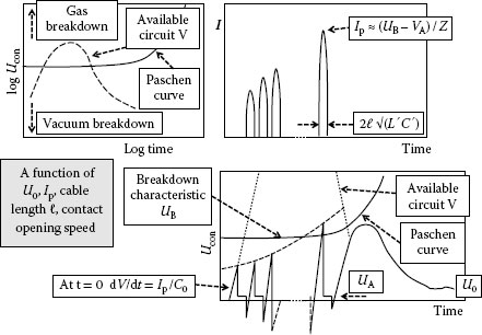
FIGURE 10.8
The development and cessation of the showering arc [16,17].
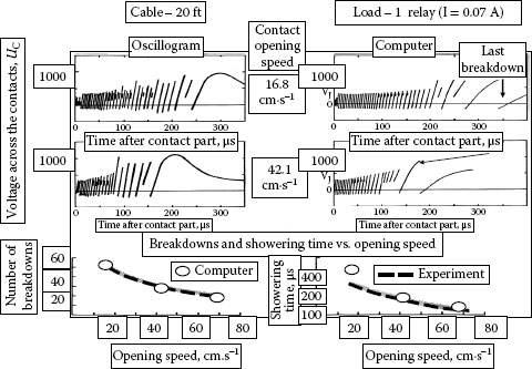
FIGURE 10.9
Comparison of the measured showering arc voltage transients with a computer model of the showering arc process [19].
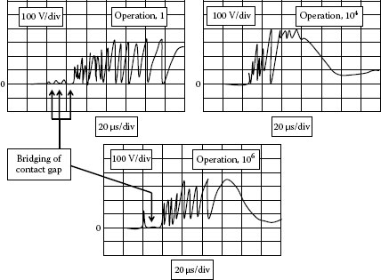
FIGURE 10.10
Changes in showering arc voltage with number of operations showing the initial bridging of the contact before the showering arc develops [18].
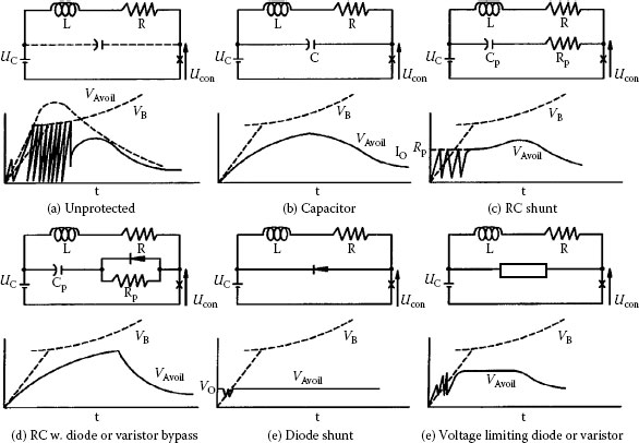
FIGURE 10.11
Possible methods of minimizing the effects of the voltage transient in low-current DC circuits [16].
10.3 Arc Erosion of Electrical Contacts
For the designer of switching devices in a circuit, one of the most important consequences of arcing is the effect the arc has on the erosion of the contact material. Contact erosion occurs because both the cathode and the anode under the roots of the stationary arcs can be heated to the boiling point of the contact material. In fact, even when the arc is forced to move rapidly across a contact surface the arc roots still melt the contact surface directly under them. The individual components that cause the heating of the contacts have already been discussed in Sections 9.5.2 and 9.5.3. Figure 10.12 presents a summary. The amount of erosion per operation of the contact depends upon many parameters as shown below:
1. The circuit current
2. The circuit resistance, inductance and capacitance
3. The arcing time
4. The contact material
5. The structure of the contact material
6. The shape and size of the contact
7. The contact’s attachment
8. The opening velocity of the contact
9. The bounce on making contact
10. The open contact gap
11. Motion of the arc on the contacts
12. The design of the arc chamber
(a) Gas flow
(b) Insulating materials used
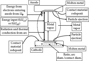
FIGURE 10.12
Energy balance at the contacts from the arc and the effect on contact erosion.
The phenomenon of contact erosion is further complicated by mechanical stresses on the contact as a result of the impact on closing. These stresses caused by the switch mechanism affect the contact materials in widely different ways which depend upon the material and the manufacturing process (see Chapter 16).
The consequences of this is while it is possible to present some general principles to let you appreciate the qualitative aspects of arc erosion, most of the design information given can only be used as a guideline. Only electrical testing of the final design of the switch will give the actual erosion the contacts will experience in that device.
To illustrate this, we can show in principle the mass lost per operation of the contact should be given by
(10.9) |
Both sides of this seemingly simple equation present complexities that prevent it from ever being established, let alone solved. For example, what is meant by the mass loss? The total mass loss from a contact is a mixture of the following components:
• Metal vapor evaporated from the arc roots +
• Metal droplets ejected from the arc roots −
• Metal re-deposited back onto the contact faces −
• Metal deposited from the opposite contact
Even in the case of a diffuse vacuum arc with Cu contacts where the erosion of the cathode [20] is given by:
(10.10) |
it has been shown w is composed of ~10% ions, ~1% neutral atoms and ~89% metal particles [21]. If the contacts are placed into a practical vacuum interrupter and operated at close contact gaps, then the transfer of contact material back and forth between the contacts results in an erosion rate of about ten times lower (× 0.1) [22,23]. The actual erosion products are, thus, difficult to predict from a given switching event even when the parameters are carefully controlled. The modeling of the total power input into the contacts also presents problems. First of all, for most designers of switches, it is only possible to measure the current in the circuit I(t) and also perhaps the arc voltage UA(t) across the contacts during the arcing. If we take some of the power input components at the cathode, (Section 9.5.2):
• Power input from ions = f1(I × cathode fall voltage)
• Power input from radiation = f2(I × UA)
• Power input from neutral atoms = f3(I × UA)
• Joule-heating of contact = f4 (I2)
Again, this is very difficult to model. Most researchers try to perform comparative studies on one contact apparatus and most designers of switches ultimately test their device to show the current interruption and number of operations that are satisfactory for a particular application. There is, however, an enormous literature on contact erosion [24], but most of it applies to specific situations and should only be used as a guide by the designer. Examples of erosion models that take into account vaporization of metal and splashing of material can be found in [25,26]. The reader is referred to Chapter 16 for a detailed discussion of contact erosion for various material compositions and for various testing conditions. The measurement of contact erosion is also briefly discussed in Sections 13.5 and 18.4.4. An example of comparative erosion data for a large number of contact types is given in Figure 10.13 [27]. Here some seemingly similar contact materials have considerably different erosion rates. The following sections give you a few parameters you need to consider and the difficulty in generalizing the measurement of arc erosion from any one set of experimental data.
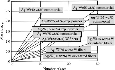
FIGURE 10.13
Comparative erosion of electric contracts [27].
10.3.1 Erosion on Make and Erosion on Break
Arcing occurs as the contacts come together by the breakdown of the contact gap before they touch each other. This arcing period depends upon the circuit voltage and closing speed of the contact, but it is usually of very short duration. Once the contacts touch, they may bounce apart again and an arc will form between them. Figure 10.14 illustrates the contact closing event: (a) An expanded view of the closing movement of the contact just before they touch, (b) The possible variations in voltage across the closing contacts with an expanded view as the contacts come together and (c) The initiation of the circuit current. As the contacts close, a pre-strike arc can occur just before the contacts touch (See Section 9.3). Once the contacts touch, bouncing can occur. In some switching devices, the total bounce time may last for milliseconds (see Section 13.7). The characteristics of the bounce will also influence the erosion of the contacts [28]. It is, therefore, possible to have as much contact erosion on make as it is on break. For the special case of contactors, the type of device that switches motors (see Sections 14.3.4 and 18.3) where the current at make is normally six times (6×) the break current, it is even possible for the erosion at make to be higher than that at break. An example of material loss or arcing time for break-only and make-only contact pairs is shown in Figure 10.15 [29]. To further complicate this discussion it is entirely possible for make and break erosion taken together to be lower than the sum of the make-only erosion and break-only erosion (see Section 18.4.4).
10.3.2 The Effect of Arc Current
Figure 10.16 shows a discontinuous erosion at ~1,000 A [30], that is, at about this current the erosion rate can increase by as much as 30 times (30 ×), so
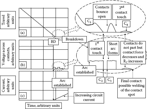
FIGURE 10.14
Schematic diagrams of contact closure showing (a) the travel and contact bounce, (b) the gap as flowing through the contacts during contact closing [91].
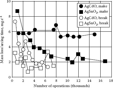
FIGURE 10.15
Erosion of silver-metal oxide contacts, break only and make only [29].
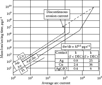
FIGURE 10.16
Discontinuous erosion of contacts at high currents [30].
(10.11) |
where kI = 0.8, I < 1,000 A and kI = 25, I > 1,000 A for Ag contacts, but kI = 0.4, I > 1,000 A and kI = 6, l > 1,000 A for Ag–CdO contacts. This effect is most probably caused by the constricting of the arc by its self-magnetic field at higher currents (see Section 9.5.1). Not only would the arc diameter become smaller but also the arc root diameter spot on both the cathode and the anode will also become smaller. The increase in the power density in the arc spots will give rise to excessive heating of the spot with the consequence that jets of metal will be ejected from the spot regions. The exponent in Equation 10.11 seems to be very dependent upon test conditions and various authors have published values in the range 1.0–3.7.
10.3.3 The Effect of Contact Size
The conduction of heat away from the contact surface is an important parameter that affects erosion. The contact’s dimensions (i.e., area, length and breadth, and thickness) are all important in assessing the probable rate of erosion. Figures 10.17 through 10.19 [31] show effects of shape and size on the erosion of Ag–W contacts one half cycle of unidirectional AC current with the polarity of the contacts fixed. It has also been shown that the discontinuous erosion can also occur at currents less than 1,000 A if the contact diameter is too small [31,32]. Borkowski et al. [33,34] again using Ag–W contacts opening a unidirectional, half cycle of AC current, show that the discontinuous erosion depends upon the contact diameter for a given current, but they plotted their data as a f(∫ldt). They show for volume of erosion ΔV of 10-mm diameter Ag contacts:
(a) For cathode erosion, ΔV=0.076(∫Idt)1.8 before the discontinuity and ΔV=0.36(∫Idt)1.28 after.
(b) For anode erosion, ΔV=1.95(∫Idt)1.4 before the discontinuity and ΔV=0.68(∫Idt)1.03 after.
They also show the temperature behind the contact face shows a steady increase as the (∫Idt) increases until the discontinuous value of (∫Idt) when it increases at a slower rate.
For currents less than 50 A, it is possible to make a conservative assessment of the contact volume required for a given application. Figure 10.20 shows an arc root on a contact surface. A rule of thumb says that the contact diameter Dc should be three times (3×) the arc root’s diameter DA and its thickness should be greater than the depth at melting of the arc which is approximately
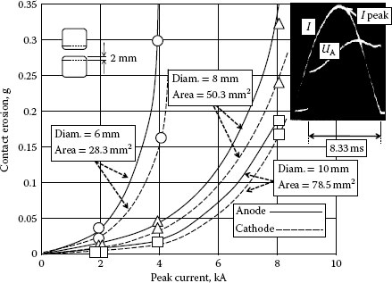
FIGURE 10.17
Contact erosion as a function of peak current, the effect of contact area, for Ag–W (50 wt.%) contacts opening at 0.5ms−1, after 5 operations and showing a typical current pulse and arc voltage characteristic [31].
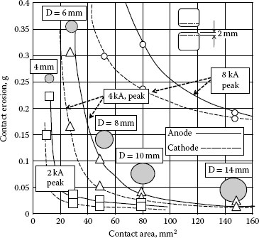
FIGURE 10.18
Contact erosion as a function of contact area for Ag–W (50wt.%) contacts for three separate peak current pulses, opening at 0.5ms−1, after 5 operations [31].
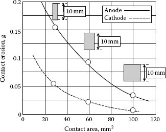
FIGURE 10.19
Contact erosion as a function of contact area and shape for Ag–W (65 wt.%) contacts, opening a current of 8kA peak, at 0.5 ms−1, after 20 operations [31].
(10.12) |
Experimentally determined arc root current densities are given in Figure 10.20, from which an arc root diameter for a given current can be calculated.
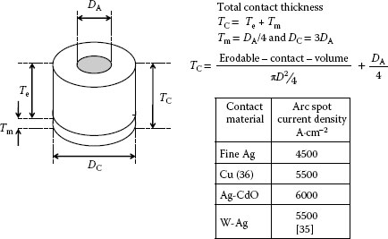
FIGURE 10.20
Erosion at the arc root and the necessary contact dimensions.
10.3.4 Determination of Contact Size in AC Operation
Let us accept the erosion data given in Figure 10.15. Also assume the arcing time at break tb on the average is one-half of the period of one half-cycle of current (i.e., 4 ms for a 60-Hz circuit and 5 ms for a 50-Hz circuit) and the bounce time on closing is tm. If the erosion rate is
(10.13) |
Then the average erosion per operation is
(10.14) |
If we assume that the contact diameter is Dc and its height is Tc, and assume the erosion is uniform, then the number of operations that can be sustained by the contact is:
(10.15) |
where δ is the density
V=πD2c4{Tc−DA4}
giving
(10.16) |
10.3.5 Erosion of Contacts in Low-Current DC Circuits
A great deal of work was performed in the 1950s and 1960s on erosion in low DC currents [36]. A lot of this work was driven by the telephone industry’s need to have relays with very long lives. In recent years, even though the logical functions of telephone relays have been taken over by electronic and optical–electronic systems, the relays still retain their safety functions (i.e., disconnecting circuits, protection from electromagnetic interference, and protection from stresses in voltage, current and temperature). In fact, the number of telecommunications relays may well be higher today than ever before. A major difference is the signal relays these days has a volume of only approximately 10 cm3 and a weight of l g compared to the 1950s relays of approximately 230 cm3 and 250 g. During this change in function and size, the relay bodies became manufactured from organic materials and the contact forces have decreased. The research activity has focused, therefore, more and more upon reliability rather than contact erosion.
In recent years, there has also been a considerable research effort to produce very reliable DC relays for automobile applications (see Sections 13.6 and 16.2.3). This has been driven by the ever increasing number and complexity of automobile electrical systems, which require reliable, long-life, low-cost relays that operate in nominally 14-V circuits and must switch currents in the range 0.1–100 A. The increase in electrical systems in cars has led to a corresponding increase in the weight of the wiring. In an attempt to reduce this added weight, the automobile companies have considered increasing the battery voltage from 14 V to 42 V. This has resulted in considerable R and D effort to develop reliable switches, relays and connectors for this DC circuit with higher voltage [37]. The 42-VDC circuit presents many challenges for the control and connecting systems. In a 14-V DC system, designing a switch to interrupt the circuit is relatively straightforward. Once the contacts have parted and the molten metal bridge has ruptured, an arc with a voltage UA ≈ 13 V appears between the contacts in less than a microsecond. This forces the circuit current to drop to the unstable Imin in a few tens of microseconds and the circuit is easily interrupted. In a 42-V DC circuit, the contacts have to open to a gap larger than 1 mm, as shown in Figure 10.21, to achieve a UA ≈ 42 V which will result in the interruption of the circuit, see Section 9.7.2 [37,38,39,40]. Figure 9.28 shows for a given contact gap, the voltage needed to sustain the arc increases as the current decreases. This figure shows for copper contacts and a 1mm contact gap, that if the current falls below about 0.5A in a 42V circuit the arc will become unstable and the circuit will be interrupted [41]. Sugiuri et al. [41] also show that a high transverse magnetic field (~200 mT) can reduce the interruption time for a slowly opening contact (10 mms−1) from 78 ms to 10 ms where the contact gap is only 0.1 mm. The disconnecting and reconnecting of connectors under load also presents a considerable challenge [42,43,44]. Not only will the resulting arc cause damage to the connector, but also to the automotive technician. Disconnecting and reconnecting loaded connectors in a 14-V circuit is relatively safe and only results in minor arcing damage.
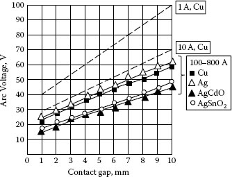
FIGURE 10.21
Expected arc voltage as a function of contact gap for currents of 1 A, 10 A (Figure 8.38) and 100–800 A [40].
In spite of the above challenges, there continues to be a need to interrupt DC currents in the range of a few tens of amperes in circuits up to and beyond 500 V [45,46,47,48]. This need is driven by the increasing application of photovoltaic solar power systems and by the expected demand for electric and hybrid vehicles. Thus, to produce switches that can generate arc voltages high enough to interrupt these circuits, renewed research and development efforts are taking place. One study by Yoshida et al. [45] uses a double-break contact system with a permanent magnet (20–30 mT) to provide a transverse magnetic field across the contacts in order to drive the series arcs away from their respective contact gaps. Figure 10.22 shows a diagram of structure of the series contact with the magnetic field and the direction of motion of the arc. It also shows the combined arc voltages and their effect on the current leading to the interruption of a 400-V, 30.2-A DC circuit with a resistive load of 13.2 Ω. At 1 ms, there is an immediate drop in current to about 28 A as soon as the two series arcs are formed and inject a back voltage of 32 V into the circuit. As the contacts continue to open, the combined arc voltage slowly increases with a corresponding slow decrease in the current. From 1 ms to 3 ms (i.e., for the first 2 ms of arcing and where each contact gap <0.72 mm), the voltage increases at a rate that is expected for a stationary arc between the two pairs of contacts opening at 0.36 ms−1. Thus, at 3 ms the current has only decreased to about 26 A. It is only when each contact gap is greater than 0.72 mm that the 20–30 mT magnetic field begins to drive the arcs off their respective contacts. This causes the arcs to lengthen, resulting in a rapid increase in the arc voltage and a corresponding rapid decrease in the circuit current. At about 5.6 ms, the arc voltage reaches 400 V and the current is being driven to zero. However, at this time (R in Figure 10.22), the field between each contact pair (~1 × 10⁵Vm−1) is high enough for the arc to re-strike and be re-established back between those contacts with a combined arc voltage of ~75 V as would be expected from the open contact gaps at that time. The circuit current now returns to the expected value of ~24.5 A. This shows an optimum arc voltage, the contact gap and the arc movement for interruption of these higher voltage DC circuits arise to prevent this re-strike phenomenon. Yoshida et al. [45] indeed show for their contact system, this re-strike phenomenon does not occur for circuit voltages up to 300 V. However, even with re-striking, they do successfully interrupt DC circuits up to 500 V with currents from 5 A to 30 A. As would be expected with a two-break system, they find that for a 50-VDC circuit, the transverse magnetic field does not have an effect on the arcing time.
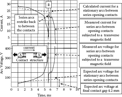
FIGURE 10.22
Interruption of a 400V/30.2 A DC circuit using a bridging contact opening at 0.36 ms−1 to produce two series arcs [45].
In Section 10.2.2 the consequences of arc voltage UA, circuit voltage UC, arc current I and circuit inductance on the duration of the arcing time ta on the contact erosion has been explored. First of all, erosion in DC circuits is complicated by the fact, for a given contact material, switching a given set of circuit conditions, will always cause a net transfer of contact material from one contact to the other. The net transfer will eventually result in a buildup of a pip on one contact and a crater on the other. Figure 10.23 [49] shows a good example of this phenomenon for an Ag contact pair. Sometimes, the net metal transfer is from the anode to the cathode (i.e., a net cathode gain). In this case, the arc is sometimes called an anode arc [36]. Sometimes, the net metal transfer is in the reverse direction (i.e., a net anode gain). In this case, the arc is sometimes called a cathode arc [36]. The direction of net metal transfer is also dependent on the contact material; so under a given set of conditions, one material will have a net transfer to the cathode (sometimes called anodic material) while another material will have a net transfer to the anode (sometimes called cathodic material).
Let us explore a qualitative explanation of these erosion characteristics. In Figures 10.2 and 10.3, we saw that the arcing time in a 6-V circuit for the gold contacts depends on the circuit inductance and the circuit current. In those experiments, the arcing time ranged from about 100 ns to 3.5 μs. As the contacts part, the molten metal bridge is drawn between them and eventually ruptures. The effects of the bridge rupture on the direction of metal transfer were hotly debated in the 1950s and 1960s. A number of thermoelectric effects such as the Thompson effect and the Kohler effect were postulated to cause a net metal transfer of eroded metal from the anode to the cathode [50,51]. Another effect postulated by Bühl discussed the possibility that the fine metal droplets that formed after the rupture of the molten metal bridge would become positively charged [51]. Electro-migration has also been postulated as a possible explanation of net metal transfer of contact material to the cathode [52]. It is now generally agreed for currents greater than Ilim (see Section 9.5.4) the effect of bridge erosion is overwhelmed by short arc erosion. It is only when the circuit current is below Ilim, that contact erosion resulting from the molten metal bridge is observed [53,54]. After the rupture of the molten metal bridge, there is a very small gap between the contacts with a metal vapor with high pressure between them. As I have discussed in Section 9.4.2 (Figures 9.17 through 9.21), initially after the rupture of the bridge, there is no conduction across the metal vapor and the voltage rises rapidly across the contact gap. It is only when the metal vapor pressure reduces to a few atmospheres that a pseudo arc forms with the current carried mainly by metal ions. Thus, during this stage the net transfer of metal would be expected to be from anode to cathode. Figure 10.24 shows that while metal is transferred both from the cathode and the anode immediately after the rupture, the net transfer is from the anode to the cathode; see Figure 10.25. This data is made possible using a radioactive tracer technique [5,55]. In Figure 10.26, the effect of the metal transfer from the pseudo arc is seen in the first 400 μs. As the contacts continue to open and the cloud of metal vapor expands, the pressure of the metal vapor continues to decrease and a normal arc will form with 99% of the current now carried by electrons [56,57,58], see Section 9.5. In this arc, the electrons liberated by the cathode will ionize the metal vapor, creating positive metal ions and will also evaporate anode material by electron bombardment. Figure 10.27 illustrates the effects at the cathode and anode [59]. The metallic ions move toward the cathode and impact on the cathode. This may erode some cathode material, but because these ions are the same material as the cathode, they have a high probability of sticking, so you would expect an accumulation of material on the cathode, that is, a net cathode gain. Figure 10.26 illustrates this metallic arc erosion during the metallic arc phase. Although both cathode and anode do gain some material from the other contact, the net effect is for the cathode to gain material.
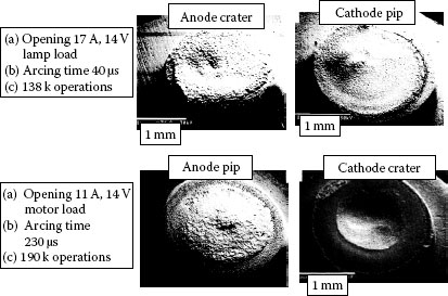
FIGURE 10.23
Pip and crater formation on a silver contact pair [49].
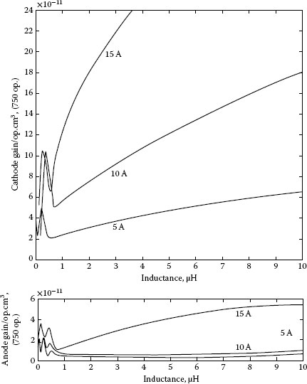
FIGURE 10.24
Absolute cathode gain and anode gain for gold contacts in a 6 V DC circuit using a radioactive tracer method showing more metal transferring from the anode to the cathode than transferring from the cathode to the anode [5].
If the arc lasts for a long enough time, the contact gap increases and the ambient gas will enter the arc. Thus, the nature of the arc changes from a metallic arc to a gaseous arc, that is, an arc where the ambient gas also becomes the dominant ionized plasma column [56,57]. This change can be observed by an increase in the arc voltage; Figure 10.28 illustrates this well [60]. This jump in voltage as the arc transitions from the metallic phase to the gaseous phase is most easily observed for low-current DC arcs. For example, in Figure 9.62 where the current is 8 A, the transition from the metallic arc to the gaseous arc is not as evident from the measurement of arc voltage. Some researchers relate further steps in this low-current arc voltage to other electron–gas interactions as the contacts continue to part [60,61,62]. In this state, the ambient gas increasingly becomes ionized. When the gas ions reach the cathode, they gain energy as they drop through the cathode fall, but now they erode cathode material and do not add material to it (see Figure 10.29). As a result as the gaseous arc continues, more material is now eroded from the cathode than from the anode and a net anode gain begins to be observed, as for example in Figure 10.30 [63]. The generalized net transfer to the cathode for arcs in DC circuits of short duration and low current is shown in Figure 10.31.
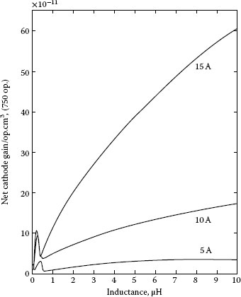
FIGURE 10.25
Net cathode gain for gold contacts in a 6-VDC circuit, from Figure 10.24.
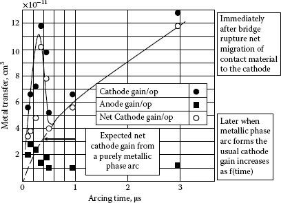
FIGURE 10.26
Cathode gain, anode gain and net cathode gain for gold contacts switching a 10 A, 6 V circuit as a function of arcing time from Figures 10.24 and 10.25.
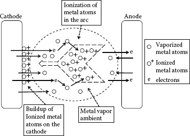
FIGURE 10.27
Contact erosion in a low-current metallic phase arc.
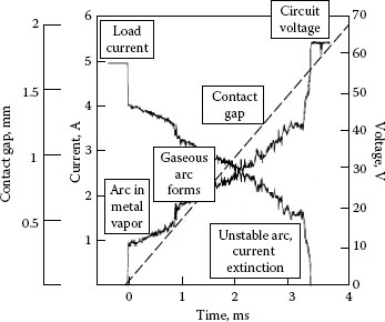
FIGURE 10.28
Voltage drop across opening silver contacts (0.5 ms−1) in a 4.9 A, 62 VDC circuit showing the transition from a metal vapor arc to a gaseous arc [60].
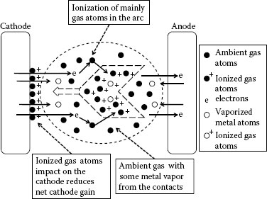
FIGURE 10.29
Contact erosion in a low-current gaseous phase arc.
The effect of this material transfer when switching DC circuits is it produces cathode pips and anode craters or anode pips and cathode craters on contacts. The exact nature of the erosion depends upon the arc duration (which, in turn, depends also upon the circuit current, inductance, and voltage) and on the contact material. Figure 10.23 [49] gives an example for Ag contacts. For an arcing time of 40 μs, a cathode pip and a slight anode crater develops, but for a longer arcing time of 230 μs (~6× longer), a very visible anode pip develops with a well-defined cathode crater. Figure 10.32 illustrates one experimental study of contact erosion for relatively long duration DC arcs switching a 60-VDC circuit [64]. At low currents (short arcing times), the metallic phase arc usually shows a net cathode gain. As the arcing time increases and the arc forms the gaseous phase, the cathode loses material and the anode gains. This continues until at the higher currents there is intense removal of metal from both the anode and the cathode. The metal transfer is also dependent upon the contact material, the contact opening speed and the finished cleanliness of the contacts. Figure 10.33 shows the effect of these parameters for one set of experimental conditions for Ag–SnO2 powder metal contacts and for Ag–SnO2–InO2 internally oxidized contacts [65].The transfer process is made more complicated if organic vapor is present, because surface activation tends to make the contacts more cathodic. Activation also tends to cause the arc roots on the contacts to jump to the carbon sites, allowing more uniform erosion over the contact surfaces and thus minimizing the effects of formation of pips and craters. Holmes and Slade [66] achieved a similar effect with silver contacts by adding a small percentage of tungsten.
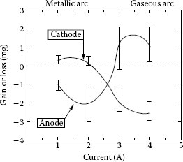
FIGURE 10.30
Net erosion characteristics of a metal vapor arc and the effect of the transition into a gaseous arc [63].
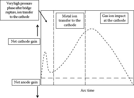
FIGURE 10.31
Generalized net cathode gain for contacts switching a short duration, low-current DC arc [5].

FIGURE 10.32
Mass transfer between contacts opening a 60 VDC circuit as a function of current i.e. arcing time [64].
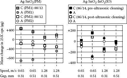
FIGURE 10.33
Comparison of material transfer of silver metal oxide contacts made by different processes and compositions opening a 20 A, 13.5 V, 0.44 mH circuit as a function of two contact opening speeds and two final contact gaps [65].
10.3.6 E rosion of Contacts in Low-Current AC Circuits
In Section 10.2.1, I stated that the average arcing time for contacts opening in AC circuits is tb=th/2, where th is one half-cycle of current. The arcing time in AC circuits is not usually dependent upon the arc voltage, because most AC switches operate at voltages greater than 100V (RMS). For some switches, the arcing time may depend upon the point on the AC wave at which the contacts open and the time from there to the first current zero when the circuit is interrupted. As shown in Section 10.3.3, at high currents there is considerable erosion from both contacts and neither has a net material transfer from the opposing contact. At lower currents, the discussion in Section 10.3.5 may have some relevance. Sharkh et al. [67] have studied the erosion of Ag–CdO contacts for determining the wave point at switching for one half-cycle of a 50-Hz unidirectional current. Their data, however, is taken with very slow contact opening of 0.1ms−1. The change in mass of the cathode and the anode contact is measured after a few thousand opening operations for contacts opening 1 ms, 3 ms, 5 ms and 7 ms after the initiation of the AC current. This results in a contact spacing at the first current zero of 0.9 mm, 0.7 mm, 0.5 mm, and 0.3 mm, respectively. Care should be taken in applying this data for general switching in AC circuits, because most AC switches open with faster opening speed (up to 1ms−1) and have larger contact gaps at current zero. The slow opening speed and the small final contact gap is most probably required to obtain consistent erosion data as Slade et al. found when measuring contact erosion opening contacts at 880 A (RMS) [68]. Figure 10.34 does show a marked dependence of the change in mass of the anode and cathode as a function of the point on the wave at which the contacts open. In an AC half-cycle, the current goes from zero to zero in a sinusoidal wave, so the point at which the contacts open not only determines the arcing time, but also determines the current level. The data in Figure 10.34 shows a general loss of metal from the cathode and a general anode gain up to 5 ms of arcing. For longer arcing times, the anode gain and the cathode loss are both reduced. In general, most AC switches have a random opening. One exception would be a switch that is opened by an AC magnetic coil, such as a motor contactor (see Chapter 14). Here, the magnetic force on the actuating armature would begin to open or release the contacts at a set position on the AC current passing through the coil. Shea [69] shows that contact erosion in a three phase vacuum contactor will be completely different from one phase to the next for a point on wave opening, but will be uniform across all three phases for a random opening (see also Section 13.6.4).
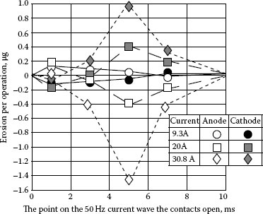
FIGURE 10.34
Effect on point-on-wave on erosion for AgCdO contacts, 240 V (RMS), opening at 0,1 ms−1, for three currents, 9.3 A, 20 A, and 30 A [67].
From Chapter 1 we know that the current flow through a pair of contacts is constricted to flow through a very small area. This is illustrated in Figure 10.35. The flow of the current along the contact surfaces gives rise to a force Fb that tends to blow the contacts apart. This force FB is given by [70,71].
(10.17) |
where μ0 is the magnetic permeability in vacuum (μ0=4π×10−7 VsA−1m−1≈1.25663702×10⁻⁶ Hm−1 or NA−2or TmA−1 or WbA−1m−1), I is the instantaneous current, R is the measured contact radius, and a is the average radius of the constriction. Using Equation 10.17 and noting that ln ln[R/a]=12ln[R/a]2
(10.18) |
where A is the total area of the contact face. The flaw in using Equation 10.18 is that as the blow-off force on the contacts increases, the contact force F decreases. Barkan [72] has considered this problem. Given that the total force on the contacts F is
(10.19) |
where FS represents the spring force holding the contacts together and FA represents a force resulting from the current flow in the whole contact structure. This force is very often arranged to be a blow-on force that can counteract FB and can usually be represented by
(10.20) |
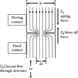
FIGURE 10.35
Contact blow-off force from the passage of current through the contact spot.
where K is a constant. Substituting for F in Equation 10.18 from 10.19 yields
(10.21) |
FB appears in both sides of this equation and the equation cannot be solved explicitly for FB. Barken put Equation 10.21 into the form
(10.22) |
and showed that if the right-hand side = α1 and the left-hand side = β1, a solution of (10.22) can be found when
α1=β1
and
dα1dFB=dβ1dFB
The second expression gives
(10.23) |
Substituting for FB in Equation 10.23 into 10.22 gives the minimum spring force required:
(10.24) |
Let us take the contact shown in Figure 10.35. Here FA = 0, so Equation 10.24 reduces to
(10.25) |
Figure 10.36 shows data for the contact force FSmin required to balance the blow-off force FB using butt contacts in high vacuum. It can be seen that Equation 10.25 correlates well with the experimental data. The curve for Equation 10.25 shown in Figure 10.36 can be represented (within the experimental error) by
(10.26) |
High currents such as these are encountered by vacuum interrupters in vacuum circuit breakers, because the testing standards require them to withstand (i.e., their single contact pair stay closed) while passing the full fault current for up to 3 s. It is, therefore, critical to have a contact force in excess of FSmin not only to keep the contacts closed, but also to provide a high enough force to maintain a low contact resistance. If the contact resistance increases too much, the contact region may melt and the contacts will weld [73]; see Section 10.5.1. The increased application of photovoltaic solar panels and the development of hybrid and electric automobiles has not only raised the interest in switching DC currents of a few hundred amperes and circuit voltages of a few hundred volts, but these switches and relays and their connections now have to withstand fault currents of a few thousand amperes without welding [74]. Figure 10.37 shows the FSmin for two relays with different contact materials: one with Cu contacts and the second with a harder Ag–Cu–Cr material. The small difference in the values would be expected from the difference in the hardness of the two contact materials (see Equation 10.25). It is interesting to note Equation 10.26 is still a good approximation for these lower currents to the values calculated from Equation 10.25.
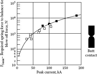
FIGURE 10.36
Minimum spring force that counters the blow-off force from the passage of high current through the contact spot [72].

FIGURE 10.37
Minimum spring force that counters the blow-off force from the passage of currents in the range 1 kA-6 kA through the contact spot [74].
If the contacts are permitted to blow open, the blow-off force will rapidly be reduced as the contacts begin to open, and other forces resulting from the formation of the arc will add to the opening force. Figure 10.38 illustrates the forces involved. Once the contacts begin to open, the contact area decreases, the region of contact melts and a molten metal bridge forms; see Section 9.4.2. If the bridge ruptures a very high pressure metal vapor region is formed between the contacts [75], which will provide sufficient force to continue the opening of the contacts. Even if the bridge does not form, a dense high pressure region can still exist between the contacts [76]. This is sometimes termed a floating arc [77]. As the contacts continue to open, an arc can form between them. The pressure from this arc can continue the contact parting [76, 78,79,80,81]. Figure 10.39 illustrates these effects [76]. In this example a high current is passed through the bridge contact shown. The spring force on the closed contacts is about 1.4 N and when they are open, it is about 1.55 N. The effect of the passage of the high current is shown in six stages: (a) The contacts are closed and the current begins to flow across them. (a)–(b) The blow-off force initially parts the contacts, and begins to diminish when the molten metal bridge forms. (b) The bridge ruptures and the high pressure metal vapor between the contacts forces one side of the bridge contact to open initiating a metallic phase arc. (c) The second contact opens forming a second series arc. (c)–(d) The pressure from these arcs continues to force the contact apart. (d)–(e) The spring force on the contacts overcomes the effect of the lower current arc and the contacts close. The repulsion force from the arc for closely spaced contacts can be roughly estimated using the analysis presented by Holmes et al. [66]. At the initial formation of the arc in Figure 10.39, (b)–(c), the arc voltage ≈15V, the average current ≈500A and its duration ≈1ms, which gives the average arc energy as 15 × 500 × 10−3 = 7.5 J. If we conservatively suppose that 10% of this energy goes into heating and expanding the ambient gas and that 1% of this gas expansion is confined by the inertia of the cold gas, then as the contacts move about 100 μm in this time the average force on the contacts is:
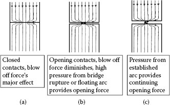
FIGURE 10.38
The forces resulting from the passage of high current through a closed contact: (a) the blow off force resulting from the passage of current through one contact region, (b) the continued opening force resulting from the formation of a high pressure metal vapor volume between the contacts in the region of the contact, (c) extension of the opening force provided by the arc which forms between the contacts.
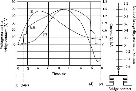
FIGURE 10.39
Contact blow open showing the voltage U across the contacts as the contacts part ‘x’ under the influence of the high current I, [76].
F=7.5×0.1×0.01100×10−6=75 N
This is certainly enough to provide the opening force to keep these contacts open. This contact blow opening may not only result in severe erosion of the contact material, but also may result in severe contact welding.
Care should be taken in interpreting Equations 10.17 and 10.26 as they only strictly apply to the butt contacts with one contact spot illustrated in Figure 10.35. If there are two contact spots, the initial blow-off force would be reduced [82]. For example, if the two contact spots are placed far enough apart and are of equal area, then the current I would be split and each spot would pass ½I. The two contact spots can be considered to be semi-independent when they are spaced more than 10 spot diameters apart [83] (i.e., for Ag contacts with a contact force of 10 N, ~1.6 mm apart and for 100 N, ~5 mm apart). The blow-off force would be:
FB=4.45×10⁻⁷{I/2}2+4.45×10−7{I/2}2=4.45×10−7{I2/2}
Some high-current switches use multiple current paths in parallel to lower the effect of the blow-off forces at each contact. A discussion of these multiple paths can be found in references [72,82,84]. Figure 10.40 shows the current distribution for ten-finger contacts. The distribution depends upon the contact resistance of each contact, its thickness, width, the distance between each contact, the thickness of the fixed bar and the length of the fingers to which the contacts are attached [85].
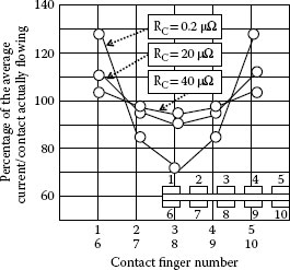
FIGURE 10.40
The current distribution of the average current in 10 contacts arranged in a knife-edge structure [85].
All contacts weld or stick to some extent. It is only when the strength of the weld prevents the proper operation of the contacts that it presents a serious problem. The formation of a weld is a complex function of the circuit current, depending on factors like whether or not arcing occurs, the contact material, the structure of the contact surface, the structure and nature of tarnish films, and the design of the structure in which the contacts operate. The weld force Fw is given by
(10.27) |
where Γ is the tensile strength of the material and Aw is the area of the weld. Now as Γ ≈ H/3, where H is the hardness, then
(10.28) |
The tensile strengths or breaking strength of a material is not an exact number, and is usually given as a range (see, for example, Table 10.4).
The elastic limit is always exceeded before the breaking stress is reached. The process of drawing a material into a wire increases its strength: in fact, the finer the wire, the greater its breaking stress. Cold-working generally tends to increase the breaking stress of the material. So even with simple equations like Equation 10.27 and Equation 10.28 you can see for any given contact system there will be a rather large variation in the measured weld force Fw.
Contact welding can occur if a high enough current passes through closed contacts and causes the contact spot to melt. Welding can also occur after an arc is initiated between contacts as they close. This arc can result from the electrical breakdown of the closing contact gap (Section 9.4.1) and it also can be continued by the contacts bouncing open once they have initially touched (see Figure 10.14).
10.5.1 Welding of Closed Contacts
If we assume that welding occurs when the contact area reaches the melting temperature Tm, then using Equation 9.41 the voltage across the closed contacts when they weld will be:
(10.29) |
TABLE 10.4
Hardness and Tensile Strength
Metal |
Hardness (108N m−2) |
Tensile Strength (108 Nm−2) |
Cu (cast) |
4–7 |
1.2–1.7 |
Cu (rolled) |
4–7 |
2.0–4.0 |
Cu wire (hard drawn) |
4–7 |
4.0–4.6 |
Cu wire (annealed) |
4–7 |
2.8–3.1 |
Ag wire |
3–7 |
2.3–3.5 |
W wire |
12–40 |
15–35 |
(10.30) |
(10.31) |
(10.32) |
if ρ is in Ωcm, H in N mm−2, F in N. Equation 10.32 can be further refined by taking into account how the physical constants change as a function of the temperature.
For example, by combining straightforward contact equations with experimental data for the contact blow-off force (Equation 10.26) and contact material hardness and resistivity data as a function if temperature, it is possible to develop an easily usable equation for the threshold welding current, Iweld, for a single region of contact as a function of the applied contact force, Fs. (where the total contact force is Ft=Fs−FB) for a single region of contact and for a current pulse of a few milliseconds: e.g. an ac current half cycle [86], see Eq. 10.33
(10.33) |
where Iweld, is in amperes, Fs in Newtons, Um is the contact material’s melting voltage (See Table 24.1A), ρ0 the resistivity in Ω.mm and H0 is the contact material’s hardness in N.mm−2 at temperature T0. Also T1 is a temperature close to, but less than the contact material’s melting temperature Tm and α is the materials temperature coefficient of resistivity. Using Equation 10.33 together with values forρ0H0Um and α found in contact material properties (See Tables 24.1A&C) values of Iewld compare well with experimental values given by in Figure 10.41.
I have found the following expression gives a quick way of making a conservative estimate for the required extra force needed to keep butt contacts together and still prevent them from welding.
(10.34) |
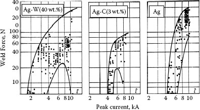
FIGURE 10.41
Welding of closed contacts showing the effect of the threshold current and the variability of the weld force for a given current [87].
Figure 10.41 illustrates the threshold current effect for a number of different contact materials [87]. Figure 10.41 also illustrates the extreme variability of the weld strength at a given current. For this reason, researchers frequently plot their weld data as a cumulative probability for a given set of circuit and contact conditions (see, for example, Figure 10.42 [88,89].
It is possible to obtain an estimate of the maximum weld force by making some simple assumptions [90]. Let us consider Figure 10.43; the volume of metal in the contact region that is melted is assumed to be a sphere whose radius a is the radius of the weld in area Aw. It is also assumed that the energy from the welding current is used for adiabatic heating of this spherical melted region. The energy Wc to melt the contact region is
(10.35) |
where m is the mass of material melted, CV the specific heat, Tm the melting temperature, Tb the initial temperature, and CL the latent heat of fusion. Now if δ is the material density, then:
(10.36) |
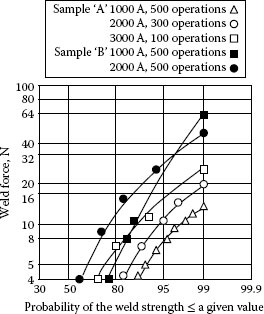
FIGURE 10.42
Cumulative weld strength of an Ag–W contact pair [88].
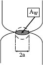
FIGURE 10.43
The weld area and the assumed spherical molten region.
Now if the weld area is assumed to be the same as the cross-section of the molten sphere, then,
(10.37) |
The weld force Fw is
(10.38) |
Using Equations 10.36 and 10.38, eliminating a,
(10.39) |
where
(10.40) |
If all the energy is used to melt the contact spot, then:
(10.41) |
where VC is the voltage measured across the contacts. Thus, combining Equation 10.39 with Equation 10.41 gives the maximum weld force for closed contacts that would be expected to occur. Examples of theoretical limits for different materials are given below:
for Ag−CdO:FW=67W2/3for Cu:FW=107W2/3
Figure 10.44 gives experimental data for these two contacts of these two materials. The experiment used closed contacts with current pulses ranging from less than 30 kA to 180 kA. The data for the Ag–CdO contacts in these experiments shows remarkable agreement with the theoretical data, but there is a 50% difference for the Cu contact material.
If the contact holding force is lesser than the blow-off force, an arc can form between the contacts. The voltage used in Equation 10.41 now has to be the arc voltage UA, and the total energy input into the contact region will be
(10.42) |
The time tc is the time the contacts are together and ta is the time the contacts are arcing.
10.5.2 Welding During Contact Closure
As discussed in Section 9.4.1, it is possible to form an arc as contacts close. Once the arc has formed, it can cause melting at the contacts. When they touch, the molten spots will freeze and a weld can form. Fortunately for most switching devices, this “pre-strike” arc is of very short duration and the welds that form are usually quite weak. The problem of welding becomes more severe if the contacts bounce open once they have initially made contact (See also Section 18.4.3). An illustration of contact closing showing a pre-strike arc and contact bounce is shown in Figure 10.14 [91]. As the contacts close a pre-strike arc can occur. Once the contacts touch, they can now bounce open. The amount of bouncing depends upon the contact material, the design of the switch and is a function of the energy in the moving contact when it makes contact. At the end even though the contacts do not bounce completely open, the contact force can still be low enough for contact melting to occur before the contacts are completely closed.
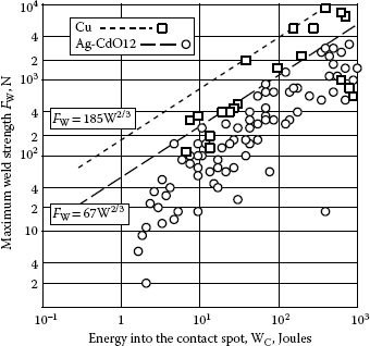
FIGURE 10.44
Weld force as a function of energy into the closed contact spot showing the maximum weld force expected for Cu and Ag–CdO(12 wt.%) contacts for high current pulses >30 kA–180 kA [92].
In order to obtain an estimate of the maximum weld strength that can be observed it is again possible to use Equation 10.39, that is,
(10.43) |
For the case of arcing between two very closely spaced contacts, an estimate for Wc is now
(10.44) |
where UA is the arc voltage and ta is the total arcing time.
Values of Fw lesser than those calculated by Equation 10.43 are frequently observed and can be explained by a combination of a number of possible physical effects. For example, if the arc roots on the contacts move, the melted spots may not be exactly opposite to each other when the contacts close, thus reducing AW. If the arc duration ta is large enough, the heating of the contact region may not be adiabatic and the heat balance described in Section 10.3 comes into effect. If the arc is very long, not all the arc energy goes into heating the contact spots. The bounce time of the contacts can be complex with the contacts opening and closing a number of times during one closing operation. Thus, the exact value of ta that affects the final melt zone is not easy to determine. Finally, the contact surface itself can be different from the bulk metal (see Section 10.6). For example, if the contact is an alloy, the composition of the surface after arc erosion may be different from the bulk contact. Thus, the value of Γ may vary considerably. Also, the surface after heating may contain inclusions of oxides or other compounds which will also change the tensile strength of the weld.
Figure 10.45 shows welding data for Ag–CdO contacts for currents ranging from 20 A to 1,200 A using a single, controlled bounce time of 0.5 ms to 5 ms [92]. Again, there is a wide range of values for weld strengths, but the maximum weld force measured gives FW=KW2/3C. Figure 10.46 gives the range over which maximum weld strengths vary for a wide range of contact materials measured under the same experimental conditions as the data in Figure 10.45 [92,93]. Except for the Ag–Ni data, the line for the maximum weld force here is close to FW≈K(WC)2/3 which is in the same form as Equation 10.39. Now, however, using a completely different experimental parameters the data for Ag-CdO gives the constant K to be between 5.2 and 7.6, whereas if we calculate a K value from Equation 10.40 for this material, we obtain a value of 67 [90]. Thus, there is a difference of a factor of 10 between the data shown in Figures 10.45 and 10.46 and the calculation using the model for closed contacts, and the previous experimental data in Figure 10.44 [90]. In an attempt to obtain a comparison of how different materials would behave under a constant bounce time, Turner and Turner [94] produced Figure 10.47. The welding of the contacts will be discussed further in Chapters 11 through 14 and in Section 18.4.3
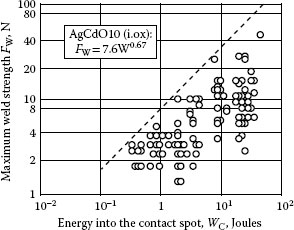
FIGURE 10.45
Weld force as a function of arc energy for a single controlled bounce, showing the maximum weld force for Ag–CdO (10 wt%) internally oxidized (i.ox) contacts [92,93].
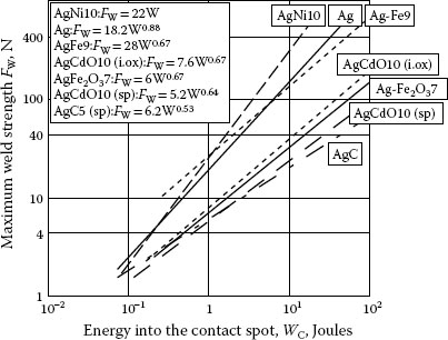
FIGURE 10.46
Maximum weld force for various metals subjected to a single controlled bounce [92,93].
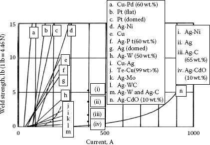
FIGURE 10.47
Comparison of weld force for various contacts of diameter 0.5 cm and with a closed contact force of 3lb (13.4N) subjected to a single controlled bounce of 3.8 ms [94].
10.5.3 Welding as Contacts Open
It is possible to observe contact welding as contacts open. This is an unusual event, but has been known to occur. It can result from a poor mechanical design for the switch that allows contact “chattering” as they open: that is, there can be contact sliding or repeated open and close operations before the contacts finally part. It can also occur from bridging of the contact gap by molten particles from the rupture of the molten metal bridge, if the contacts open too slowly (i.e., less than 0.1 ms−1). Zhao et al. [95] have demonstrated the effect of welding as contacts open for load currents of 50 A and 60 A in a 28-V DC circuit. They show the occurrence of such welds increases after a few thousand open and close operations.
10.6 Changes in the Contact Surface as a Result of Arcing
Each arcing event will change the structure of the contact surfaces. We have already discussed contact erosion which is usually the most visible and disruptive effect of arcing. However, other effects can also be identified. The arc melts the contact surface and when the surface solidifies, its make-up can change. This is well illustrated for the arc in atmospheric air for Ag–SnO2 and Ag–SnO2–InO2 contacts; see Figure 10.48 [96]. This figure shows the surface and the internal structure of the two contacts after they have interrupted the current five times. The surface of the Ag–SnO2 contacts shows gas voids and a pronounced segregation of the Ag from the SnO2. The surface of the Ag–SnO2–InO2 contacts again exhibits a porous surface, but now the oxides are still embedded in the Ag matrix. Similar changes in the surface structure of other contacts after arcing in air have also been seen: Ag–Cd–O is a good example [97].
For contacts opening in air, the possible changes in the surface structure of the contacts can become quite complex. There are many possible interactions between the arc, the contact surface and the constituents of the air. Figure 10.49 illustrates some of the possible interactions. In “clean” air, the hot contact surface and the air can form oxides, nitrides and carbonates (from CO2). If the air has industrial pollution such as SO2, H2O, chlorine compounds and dust, it is possible to form sulfides and chlorides. Organic vapor, as we have already seen (Section 10.2.3) can result in activation of the surface. Finally, if vapor from high-temperature silicone oils, grease and sealing compounds interacts with the arc, it is possible to form silica (SiO2) and C on the contact surfaces.
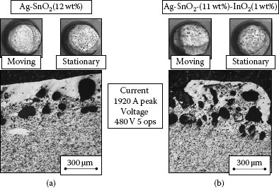
FIGURE 10.48
Change of the surface structure of Ag-SnO2 and Ag-SnO2-InO2 contacts interrupting 1920 A, 400V AC in air [96].
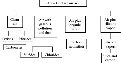
FIGURE 10.49
Possible interactions of electric contacts and the ambient air during arcing.
These surface interactions generally result in a change in the contact resistance. Possible changes in contact resistance Rc are illustrated in Figure 10.50. This figure shows how complex the changes can be. Depending upon the actual mechanical operating system, the ambient atmosphere, the contact material and the arc characteristics, it is possible for Rc to increase, decrease, or remain unchanged. For example, oxide films formed by arcing during interruption of the current can be ruptured mechanically when the contacts close when sufficient force is applied and if there is a sliding action after the contacts touch. This is what high-power molded case circuit breakers rely upon when they use Ag–W as a contact material (see Chapter 14). Contact erosion also can drastically change the Rc. For example, it is possible to erode so much of the contact surface during each arcing operation that a new contact surface of virgin metal is exposed each time, and will thus maintain a low Rc. Once a surface film has formed on the contact and the Rc increases, even a low current flowing through the closed contact can result in an increased temperature at the contact spots and this, in turn, can result in additional film formation.
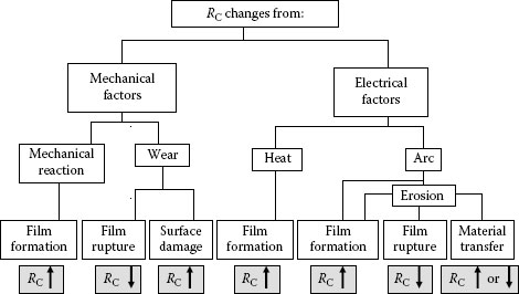
FIGURE 10.50
Possible changes in constant resistance, Rc.
For pure silver contacts and silver metal oxide contacts (Ag–MeO), such as, Ag–CdO and Ag–SnO2, the effects shown in Figure 10.50 depend greatly upon the power level (i.e., current and voltage) of the electric circuit and the forces exerted by the switch mechanism. For most devices operating at 50 A and greater, the closed contact force and the contact wipe on closing is usually enough to rupture any surface oxides and sulfides that may form. The major concern for switch designers for devices that operate in this power range are contact erosion (i.e., operating life) and contact welding.
At lower currents, where the contact forces are lower, it is possible to form surface films that result in high Rc. Figure 10.51 shows an example of changes in Rc for silver contacts switching a low current in N2 and N2 plus O2 [98]. These authors attributed these variations in Rc to the formation of an oxide layer. In an interesting set of experiments comparing filtered laboratory air and artificial air (N2 and O2 mixture), Witter and Polevoy [99] have shown that it is possible to form silver carbonate on the contact surface from the CO2 present in air. By varying the arc duration by alternatively switching an inductive and resistive load, these authors showed that at long arc times where a gaseous arc predominates, the probability that carbon and oxygen in the arc will react with either the small amount of silver vapor in the arc or with the hot silver in the arc root region to form AgCO2 is high. If the arc is of short duration, however, and the metallic arc dominates, the presence of greater density of silver vapor in the arc limits the formation of AgCO2 and, indeed, the arc roots also evaporate any carbonate that has already formed on the contact surface (see Figure 10.52) (see also Section 16.2).
10.6.2 Silver-Refractory Metal Contacts
The advantages and disadvantages of silver–refractory contacts are illustrated in Figure 10.53 [100]. It is generally agreed this class of material is more resistant to arc erosion than all other contact materials and the brittle nature of the refractory metal and the metal matrix structure makes it weld-resistant. This mixture is, therefore, the contact of choice for those devices that have to interrupt very high short-circuit currents. The most common contact mixture is a mixture of silver and tungsten. The advantages of this class of contact material, the erosion and weld resistance, however, have to be balanced against their tendency for formation of oxides and the resulting high Rc. When W–Ag materials are switched in air, tungsten oxides and silver tungstates are formed on the contact surfaces [101,102,103]. Their presence is usually observed by measuring an increase in Rc. The probability of formation of oxides in the region of contact, however, can vary widely from one operation of the contact to another [103,104], and it also depends strongly upon the contact force and upon the mechanical wiping action in the switching system studied. It is not surprising then that quantitative Rc values from one researcher to another can be quite different. Witter and Abele [105] observed a monotonic decrease in Rc after 4,000 operations at 20 A as the silver content of the tungsten–silver contacts increased (see Figure 10.54). They also showed the finer the starting powders, the higher the Rc (see Figure 10.54). Leung et al. [106] also showed a decrease in Rc values for tungsten–silver contacts, but little effect of manufacturing method was evident (see also Figure 10.54). Lindmayer and Roth [104] showed how the parameter of contact diameter can markedly affect the measured Rc. When their contact erosion data (see Figure 10.55) is superimposed upon their Rc data (Figure 10.56), it can be seen immediately that there is a correlation between the current at which the onset of the excessive erosion occurs and that at which Rc begins to decrease. The increased erosion permits enough free silver onto the contact surfaces to allow a high probability of silver-to-silver contact and hence a low Rc value. These researchers confirmed the effect of erosion on Rc when they showed at 1,000 A, for 6-mm diameter contacts, W–Ag, which had a higher erosion than WC–Ag, also had a lower Rc. These data contrast with my experiments [107] using contacts with a diameter of 4 mm and a current of 20 A, where excessive erosion was not a concern. I showed no difference between Rc values for W–Ag and WC–Ag. Leung and Kim [108] found lower Rc values at 30 A for WC–Ag contacts than for W–Ag, even though the erosion rate for W–Ag is higher than that for WC–Ag contacts. When Co or Ni is added to W–Ag or WC–Ag, the Rc tends to be somewhat lower [109,110]. This may be the result of a somewhat increased erosion rate. There are other chemical effects of these additives, however, that have been identified [107,108] and which may slow down the formation of surface oxides. On the other hand, Witter [110] showed that when the additive Ni is used in high concentrations, the formation of Ni–W phases and Ni–W oxides gave rise to a rapidly deteriorating Rc.
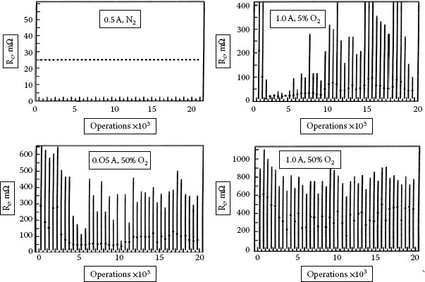
FIGURE 10.51
Example of contact resistance variations for silver contacts operating in nitrogen and nitrogen containing oxygen as a function of the number of switching operations [98].
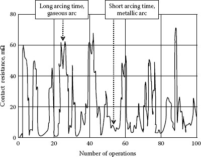
FIGURE 10.52
Contact resistance changes of closed silver contacts resulting from the formation and evaporation of AgCO2 films after long arc times and short arc times [99].
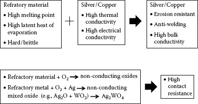
FIGURE 10.53
The silver–refractory metal contact system.
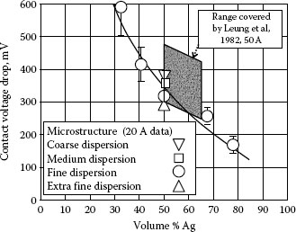
FIGURE 10.54
Contact resistance changes as the Ag content of W–Ag contacts is varied [105,106].
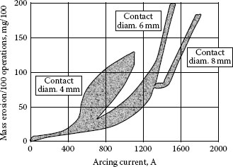
FIGURE 10.55
Erosion of W–Ag contacts and effect of contact diameter [104].
Experiments have been made with the alloy (W, Ti) C in an effort to produce a contact material which is an improvement over W–Ag [111,112]. Contacts made from (W, Ti) C–Ag showed excellent Rc values when switched up to 3,000 operations at 20 A (see Figure 10.57). Doremieux et al. [111] also showed low Rc values for this number of operations, but when they attempted to use this material for contactor applications, they obtained high Rc values after 20,000 operations at 20 A. When these contact switched high short-circuit currents [111] their surfaces were left with a thin, uniform, hard crust that contained mainly (W, Ti) with a high concentration of oxygen, either dissolved in the metal matrix or as suboxides of titanium and tungsten. This layer is practically devoid of silver and high Rc values are observed. The effects of the refractory oxides could be reduced by increasing the silver content (see Figure 10.57) and by allowing the contacts to erode more rapidly under short-circuit arcing, but these contacts had an increased probability of welding [112].
The long-term effects of passage of low current (20 A) through W–Ag contacts has also been investigated [113]. Both the contact’s voltage drop Vc and the temperature rise of the stationary contact arm were continuously measured. Four characteristic voltage types were recorded (Figure 10.58): Type 1, a steady voltage less than 100 mV; Type 2, a voltage plateau (range 150–600 mV) with frequent, rapid excursions to lower values; Type 3, rapid voltage oscillations (as much as ±100 mV) superimposed upon a slower varying mean (≈400 mV); and Type 4, extreme Type 3 (peaks as high as 1.3 V) with sudden excursions to a lower plateau (≈300 mV). I analyzed the data in terms of the expected temperature of the contact spot, the formation and decomposition of silver tungstates, and the volatility of W-oxides above 1,000°C. I showed that W–Ag can exhibit a self-limiting contact resistance. In other words, no thermal runaway is observed for the limited experimental conditions used. Further experiments with high silver content in WC–Ag–C contacts showed much lesser Vc activity. The increased silver content and the reducing effect of the carbon may limit the formation and stability of any silver tungstate or tungsten oxide. The reducing effect of carbon has been demonstrated by Lindmayer and Shroeder [114], who investigated Ag–C (3 wt% C) operated against W–Ag (35 wt% Ag). For an Ag–C cathode the Rc remained less than 0.1 mΩ, but when Ag–C was the anode the Rc was a much higher value but still lower than that of two W–Ag contacts. They attributed this polarity effect to the fact the Ag–C as cathode had much greater erosion than the Ag–C as anode, and hence the reducing atmosphere of C and CO was much greater (see also Section 16.3). Testing of various compositions of Ag–C and Ag–WC–C contacts for anti-welding, arc erosion, mechanical impact strength and interruption, showed that no one material worked best for all categories [115]
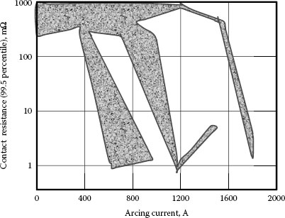
FIGURE 10.56
Effect of contact erosion from Figure 10.54 on the contact resistance of W–Ag contacts [104].
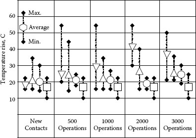
FIGURE 10.57
A comparison of the average, maximum, and minimum temperature rise for (W, Ti) C–Ag (V, 35 wt% Ag), (Δ, 50 wt% Ag), (⚬, 65 wt% Ag), and (◻ pure Ag) contacts switching 20 A AC as the number of switching operations increases [112].
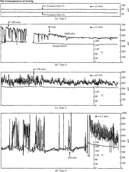
FIGURE 10.58
Possible voltage drop across closed W–Ag contacts reflecting changes in the surface chemistry of the contacts [113].
There is a well-researched body of knowledge dating back to the 1960s [116] on the deleterious effect of silicone vapors from silicone sealants, greases and oils on switching contacts. When the adsorbed silicone molecules on the contact surfaces are subjected to the electric arc, SiO2 and C are formed. Contacts switching in such an ambient eventually form a high-resistant surface, which eventually results in the failure of the switch [116,117,118,119,120,121,122,123,124]. Demethyl silicones can be represented by ((CH3)2SiO)n where n is the degree of polymerization [123]. For Dn where n < 3 the silicone is highly volatile, but for Dn where n > 5 the evaporation rate is extremely low. Tamai [123] experimented with the D4 compound, a liquid, which gradually evaporates at room temperature. D4 is an unreactive residual silicone in silicone rubbers, sealants, potting compounds and greases, which gradually is released by them into the surrounding ambient. So, for sealed or even covered switches, it is possible to gradually develop a silicone vapor concentration surrounding the switch’s contacts. When coupons of Au and Ag are exposed to D4 in a sealed chamber, a silicone film gradually forms on them. Figure 10.59 shows this for two concentrations of D4; 1,300 ppm and 7 ppm [123]. The film reaches a thickness limit of ~1.3 nm for both concentrations: in ~10 hours for the concentration of 1,300 ppm and ~800 hours for the 7ppm concentration. The process of film formation on the contact surfaces is quite complex. It has been discussed by Tamai for the D4 compound. As shown in Figure 10.60a, when the D4 silicone molecule lands on a metal’s surface it is adsorbed as a result of its O atom attaching to the dangling bonds on the metal’s surface. This new molecule on the metal’s surface is most probably a volatile liquid and can easily evaporate back into the ambient environment. Thus, the process shown in Figure 10.60a can go back and forth between the metal surfaces and the ambience. However, as Figure 10.59 shows, a surface layer does eventually form on a metal’s surface. Figure 10.60b shows if an O2 molecule is absorbed by the liquid silicone on the contact surfaces it changes the nature of the film. It eventually forms into a polymerized film that no longer evaporates. When this film is subjected to the electric arc, SiO2 and C are formed which deposit onto the contact surfaces. Discussions on the effects of this phenomenon will also be presented in Chapter 19, Section 19.4. The effects of activation on arc duration and contact erosion have already been discussed in Section 10.2.3. Further discussion of the effects of activation will also be presented in Chapter 19, Section 19.2.
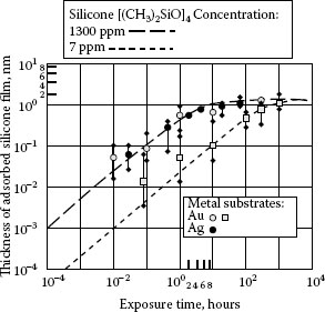
FIGURE 10.59
The growth of film thickness on the surfaces of Au and Ag coupons as a function of time in an air and two concentrations of D4 silicone ambient [123].
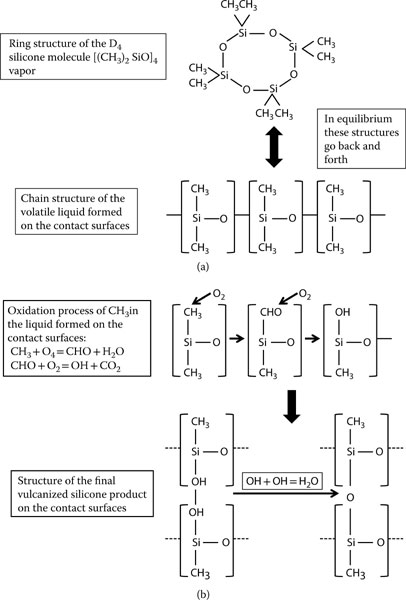
FIGURE 10.60
(a) The equilibrium reaction of D4 on a metal’s surface, (b) The oxidation and the polymerized film formation on the metal’s surface. [124].
I am extremely grateful to Professor Werner Rieder who critically reviewed this chapter for the first edition. His attention to scientific detail, his many suggestions for changes, and his encouragement, improved its substance and breadth. I also wish to thank CH Leung, who gave me the photographs used in Figures 10.23 and 10.47.
1. A Greenwood, Electrical Transients in Power Systems, 2nd ed, New York: Wiley, 1991.
2. R Garzon, High-Voltage Circuit Breakers: Design and Application, New York: Marcel Dekker, 1997.
3. PG Slade, The Vacuum Interrupter: Theory, Design and Application, New York: CRC Press, 2008.
4. WB Ittner, Bridge and short arc erosion of copper, silver and palladium contacts on break, J Appl Phys 27 (4): 382–388, 1956.
5. PG Slade, Current interruption in low voltage circuits, IEEE Trans Parts Hybrids Packaging PHP-5 (1): 56, 1969.
6. A Vassa, E Carvou, S Rivoirard, L Doublet, C Bourda, D Jeannot, P Ramoni, N Ben-Jemaa, Magnetic blowing of break arcs up to 360 VDC, Proc 56th IEEE Holm Conf Elect Cont 96–100, 2010.
7. E Gauster, W Rieder, Back-commutation in low voltage interrupters: influence of recovery time, geometry, and materials of contacts and walls, Proc 43rd IEEE Holm Conf Elect Cont 91–96, 1997.
8. A Lee, PG Slade, KH Yoon, J Porter, J Vithayathil, The development of a HVDC SF6 Breaker, IEEE Trans Power App Syst PAS-104 (10): 2721–2730, 1985.
9. JG Gorman, CW Kimblin, RE Voshall, RE Wien, PG Slade, The interation of vacuum arcs and magnetic fields with applications, IEEE Trans Power App Syst PAS-102 (2): 257–266, 1983.
10. LH Germer, JL Smith, Activation of electrical contacts by organic vapors, Bell Syst Tech J 36: 769–812, 1957.
11. http://en.wikipedia.org/wiki/Fullerene
12. EW Gray, TA Uhrig, GF Hohnstreiter, Arc durations as a function of contact metal and exposure to organic contaminants, J Appl Phys 48 (1): 1977.
13. EW Gray, How organic vapors cause contact activation, Insulation/Circuits, March 1977.
14. S Shimada, Y Takenaka, K Funaki, Effects of various organic vapors on contact resistance, Proc 17th Int Conf Elect Cont, Mano R&D Tech Center, Nagoya, Japan, 159–167, July 1994.
15. CN Neufeld, WF Rieder, Carbon contamination of contacts due to organic vapors, IEEE Trans Components, Packaging Manuf Technol—Part A 18 (2): 399–404, 1995.
16. HN Wagar, Contact and connection technology, In Integrated Device and Connection Technology, Englewood Cliffs: Prentice-Hall, 439–654, 1971.
17. HN Wagar, Predicting the erosion of switching contacts that break inductive loads, Holm Seminar on Electric Contact Phenomena 95–102, 1968.
18. K Miyajima, S Nitta, A Mutoh, A proposal on contact surface model of electromagnetic relays—based on the change in showering arc waveforms with the number of contact operations, IEICE Trans on Elect E81-C (3): 399–407, 1998.
19. CW Mills, The mechanisms of the showering arc, IEEE Trans Parts Hybrids Packaging PHP-5 (1): 47–55, 1969.
20. CW Kimblin, Erosion and ionization in the cathode spot regions of vacuum arcs, J Appl Phys 44: 3074–3081, 1973.
21. DT Tuma, CL Chen, DK Davis, Erosion products from the cathode spot region of a copper vacuum arc, J Appl Phys 49: 3821–3829, 1978.
22. MB Schulman, JA Bindas, PG Slade, Effective erosion rates for selected contact materials in low voltage contactors, IEEE Trans Components Packaging Manf Techn—Part A 18 (2): 329–333, 1995.
23. MB Schulman, PG Slade, L Loud, Influence of contact geometry on effective erosion of Cu-Cr, Ag-WC and Ag-Cr vacuum contactor materials, IEEE Trans Components Packaging Techn 22 (3): 405–413, 1999.
24. See for example the many papers on contact erosion published in the Proceedings of the Holm Conference on Electric Contacts 1951 to the present and the International Conference on Electrical Contacts from 1961 to the present. All of these papers now available on a DVD edited by Th, Schoepf available from VDE Verlag GMBH (ISBN 978-3-8007-3365-1). Since the late 1960s a number of these papers have been published in IEEE Trans PHP, IEEE Trans CHMT, and IEEE Trans CPMT.
25. F Pons, An electrical arc erosion model valid for high currents: vaporization and splash erosion, Proc 54th IEEE Holm Conf Elect Cont 9–14, 2008.
26. P Borkowski, A computer program for calculation of electrode mass loss under electrical arc conditions, Proc 23rd Int’l Conf on Elect Cont 354–360, 2006.
27. HW Turner, C Turner, Contact materials, their properties and uses, Electrical Times, Part 2, August, 277, 1967.
28. E Hetzmasnnseder, W Rieder, The influence of bounce parameters on the make erosion of silver metal-oxide contact materials, IEEE Trans Components Packaging Manuf Technol—Part A 17 (1): 8–16, 1994.
29. W Rieder, V Weichsler, Make erosion mechanism of AgCdO and AgSnO2 contacts. IEEE Trans Components, Hybrids Manuf Technol 15 (3): 332–338, 1992.
30. HW Turner, C Turner, Discontinuous contact erosion. Proc 3rd Int’l Research Symp on Elec Cont Phen 309–320, 1966 and The erosion of heavy current contacts and material transfer produced by arcing. Proc 4th Int’l Res Symp on Elec Cont Phen 196–200, 1968.
31. E Walczuk, Arc erosion of high current contacts in the aspect of CAD of switching devices. Proc 38th IEEE Holm Conf on Elect Cont, IEEE Cat No 92CH31 25–2, 1–16, October 1992.
32. AM Abdul Assis, A Erk, M Schmeizle, Andert sich der Abbrand von Schaltstucken mit wach-sendem Ausschaltstrom sprunghaft? ETZ-A, 94 (H.4): 239–240, 1973.
33. P Borkowsko, E Wulczuk. Temperature rise behind fixed polarity Ag-W contacts opening on a half cycle of high current and its relationship to contact erosion, Proc 22nd Int’l Conf on Elect Cont 334–340, 2004.
34. P Borkowski, M Hasegewa. Arc erosion of polarized contacts Ag-W by high current, IEICE Trans on Elect E93-C (9): 1416–1423, 2010.
35. K Ioyama, T Yanobe, Estimation for the spot size of short gap discharge in near one atmosphere pressure, IEICE Trans on Elect E82-C (1): 55–59, 1999.
36. LH Germer, Physical processes in contact erosion, J Appl Phys 29 (7): 1067–1082, 1958.
37. T Schoepf, Electrical contacts in the automotive 42VDC power net, Proc 21st Int’l Conf on Elect Cont 43–55, 2002.
38. L Doublet, N Ben-Jemaa, F Hauser, D Jeannot, Electrical arc phenomenon and its interaction on contact materials at 42VDC for automotive applications, Proc 50th IEEE Holm Conf Elec Cont 8–14, 2004.
39. T Schoepf, W Rieder, Consequences for automotive relays of a 42VDC network in vehicles, IEEE Trans Components Packaging Technol 23 (1): 177–182, 2000.
40. T Klonowski, R Andlauer, T Leblanc, F Faure, R Meyer, P Testé, High intensity contact opening under DC voltages, Proc 50th IEEE Holm Conf Elec Cont 459–466, 2004.
41. T Sugiura, J Sekikawa, T Kubono, Break arcs driven by transverse magnetic field in a DC 48V/6-24A circuit, IEICE Trans on Elect E94-C (9): 1381–1387, 2011.
42. T Schoepf, Disengaging connectors under 42VDC loads, Proc 48th IEEE Holm Conf Elec Cont 120–127, 2002.
43. T Schoepf, Unplugging of connectors under load in 42VDC power networks for vehicles, VDE-Fachbericht 57: 11–20, 2001.
44. J Razafiarivelo, M Porte, N Ben-Jemaa, Evaluation of arcing damage on connectors for 42VDC, Proc 50th IEEE Holm Conf Elec Cont 15–21, 2004.
45. K Yoshida, K Sawa, K Suzuki, M Watanabe, H Daijima, Influence of voltage and current on arc duration and energy of DC electromagnetic contactor, Proc 57th IEEE Holm Conf Elec Cont 17–21, 2011.
46. A Vassa, E Carvou, S. Rivoirard, L Doublet, C. Bourda, N Ben-Jemaa, DC-blowing under pulsed magnetic field, Proc 26th Int’l Conf on Elec Cont 23–29, 2012.
47. Y Liu, Z Li, K Wang, R Wang, Experimental study of arc duration under external transverse magnetic field in a dc 580V circuit, Proc 26th Int’l Conf on Elec Cont 30–34, 2012.
48. T Shrank, E.-D. Wilkening, M Kurrat, F Gerdinand, P Meckler, Breaking performance of a circuit breaker influenced by a permanent magnet field at DC voltages up to 450V, Proc 26th Int’l Conf on Elec Cont 35–40, 2012.
49. CH Leung, A Lee, Contact erosion in automotive dc relays, IEEE Trans Components Hybrids Manuf Technol CHMT-14 (1): 101–108, 1991.
50. R Holm, E Holm, Electric Contacts: Theory and Applications. New York: Springer-Verlag, 4th ed. 2000, Chap. 65.
51. F Llewellyn-Jones, The Physics of Electrical Contacts. Oxford: Clarendon Press, 1957, Chap. IV.
52. R Timsit, Electro-migration in a liquid metal bridge before contact break, Proc 56th IEEE Holm Conf Elec Cont 564–569, 2010.
53. K Hiltmann, A Schumacher, K Guttmann, E Lemp, H Sandmaier, W Lang, New micromechanical membrane switches in silicon technology, IEEE Trans Components Packaging Technol 25 (3): 397–401, 2002.
54. JW McBride, L Jiang, C Chianrabutra, Fine transfer in electrical switching contacts using gold coated carbon nano-tubes, Proc 26th Int’l Conf on Electric Contact Phen 353–358, 2012.
55. F Llewellyn-Jones, MR Hopkins, CR Jones, Measurement of metal transfer in electrical contacts by radioactive tracer method, Brit Jour Appl Physics 12 (9): 485–489, 1961.
56. PJ Boddy, T Utsumi, Fluctuations of arc potential caused by metal vapor diffusion in arcs in air, J Appl Phys 42: 3369–3373, 1971.
57. EW Gray, Some spectroscopic observations of the two regions (metallic vapor and gaseous) in break arcs, IEEE Trans Plasma Science 1: 30–33, 1973.
58. PG Slade, Opening contacts: the transition from the molten metal bridge to the electric arc, IEICE Trans on Elect E93-C (6): 1380–1386, 2010.
59. Z-K. Chen, H Mizukoshi, K Sawa, Contact erosion patterns of Pd material in dc breaking arcs, IEEE Trans Components, Packaging Manuf Technol—Part A 17 (1): 61–67, 1994.
60. SMS Sharkh, JW McBride, Voltage steps in atmospheric low current arcs between opening silver metal contacts, Proc 43rd IEEE Holm Conf Elec Cont 233–237, 1997.
61. N Ben-Jemaa, JL Queflelec, D Travers, Some investigations on slow and fast arc fluctuations for contact materials proceeding in various gases and direct currents, Proc 36th IEEE Holm Conf Elec Cont 18–24, 1990.
62. H Hoft, N Vogel, Potential steps during initial stages of short and medium arcs, Proc 13th Int’l Conf on Elec Cont 59–63, 1986.
63. Z-K. Chen, K Sawa, Effect of arc behavior on material transfer: a review, Proc 42nd IEEE Holm Conf Elec Cont 238–251, 1996.
64. J Swingler, JW McBride, A comparison of the erosion and arc characteristics of Ag-CdO and Ag-SnO2 contact materials under DC break conditions, Proc 41st IEEE Holm Conf Elec Cont 381–392, 1995.
65. Z-K. Chen, G Witter, A comparison of contact erosion for opening velocity variations for 13.5 volt circuits, Proc 52nd IEEE Holm Conf Elec Cont 15–20, 2006.
66. FA Holmes, PG Slade, Suppression of pip and crater formation during interruption of alternating currents, IEEE Trans Components, Hybrids Manuf Technol CHMT-1: 59–65, 1978.
67. SM Sharkh, JW McBride, A comparison between ac and dc erosion of Ag-CdO contacts, 17th Int’l Conf on Elec Cont 569–576, 1994.
68. PG Slade, R Kossowsky, R Aspden, R Bratton, The use of ceramic matrices infiltrated with silver for electric contact applications, IEEE Trans Parts, Hybrids Packaging PHP-10 (1): 37–42, 1974.
69. J Shea, Modeling contact erosion in three phase vacuum contactors, IEEE Trans CPMT—Part A 21 (4): 556–564, 1998.
70. R Holm, E Holm, Electric Contacts: Theory and Application. New York: Springer-Verlag, 1967, Chap. 11.
71. AC Snowdon, Studies of electromagnetic forces occurring at electrical contacts, AIEE Trans 80: 24–28, 1961.
72. P Barkan, A new formulation of the electromagnetic repulsion phenomenon in electric contacts at very high currents, Proc 11th Int’l Conf on Elec Cont 185–188, June 1982.
73. PG Slade, ED Taylor, RE Haskins, Effect of short circuit duration on the welding of closed contacts in vacuum. Proc 51st IEEE Holm Conf Elec Cont 69–74, 2005.
74. E Carvou, N Ben-Jemaa, B Mitchell, C Gautherot, J Rivene, L Colchen, Contact behavior of electrical vehicle battery junction box under high shorting and breaking current, Proc 26th Int’l Conf on Elec Cont 151–155, 2012.
75. PG Slade, Opening electrical contacts: the transition from the molten metal bridge to the metallic phase, Proc 24th Int’l Conf on Elec Cont 1–6, 2008.
76. M Bizjak, S Karin, H Nouri, Influence of vapor pressure on the dynamics of repulsion by contact blow off, Proc 21st Int’l Conf on Elec Cont 268–275, 2002.
77. BF Huber, An oscilloscope study of the beginning of a floating arc, Proc Holm Sem on Elect Cont (IIT), 141–152, November 1967.
78. JJ Shea, Blow-open forces on double-break contacts, IEEE Trans Components, Packaging Manuf Technol—Part A 17 (1): 32–38, 1994.
79. X Zhou, P Theisen, Investigation of arcing effects during contact blow open process, Proc 44th IEEE Holm Conf Elec Cont 100–108, 1998.
80. A Krätzcschmar, R Herbst, V Kulinovich, F Nothnagel, F Berger, Gas dynamic processes as the main reason for contact levitation in switching of high operating overload currents, Proc 24th Int’l Conf on Elec Cont 317–323, 2008.
81. JP Chaberie, P Testé, R Andlauer, T Leblanc, J Devautour, JP Guerry, Experimental study of contact opening, Proc 41st IEEE Holm Conf Elec Cont 194–199, 1995.
82. Y Kawase, H Mori, 3-D element analysis of electrodynamic repulsion forces in stationary electrical contacts taking into account asymmetric shape, IEEE Trans on Magnetics 33 (2): 1994–1999, 1997.
83. RD Malucci, The effects of current density variations in power contact interfaces, Proc 57th IEEE Holm Conf Elec Cont 55–61, 2011.
84. PG Slade Chapter 15, 586-59 in TE Browne. Circuit Interruption, Theory and Techniques. New York and Basel: Marcel Dekker, 1984.
85. Y Yoshioka, Calculation of current distribution in heavy current contacts with many parallel fingers, Proc 7th Int’l Conf on Elec Cont 382–388, 1974.
86. PG Slade, The current level to weld closed contacts, Proc. 59th IEEE Holm Conf. on Electrical Contacts, 2013.
87. E Walczuk, Welding tendency of closed contacts, Metall 4: 381–384, 1977.
88. PP Koren, PG Slade, CY Lin, Welding characteristics of Ag–W contacts under high-current conditions, IEEE Trans Components Hybrids Manuf Technol CHMT-3 (1): 50–55, 1980.
89. E Geldner, W Haufe, W Reichel, H Schreiner, Schweisskraft von Reinsilber, Reinkupferund verschiederen Kontakwerkstoffer auf Silberbasis, ETZ-A 93: 216–306, 1972.
90. M Bet, G Souques, Behaviour of electrical contacts under current waves of great intensity. Proc 10th Int’l Conf on Elec Cont Phen Budapest, 23–34, 1980.
91. S Kharin, H Nouri, D Amft, Dynamics of arc phenomena at closure of electrical contacts in vacuum circuit breakers, IEEE Trans Plasma Science 33: 1576–1581, 2005.
92. E Walczuk, D Boczowski, Computer controlled investigations of the dynamic welding behavior of contact materials, Proc IEEE Holm Conf on Elec Cont 11–16, October 1996.
93. E Walczuk, D Boczowski, D Wojcik, Electrical properties of Ag-Fe and Ag-Fe2O3 composite contact materials for low voltage switchgear, Proc 24th Int’l Conf on Elec Cont 48–54, 2008.
94. HW Turner, C Turner, Contact materials, their properties and uses. Electrical Times, Part 3, 313, 1967.
95. L Zhao, Z Li, H Zhang, M Hasegawa, Random occurrence of contact welding in electrical endurance tests, IEICE Trans on Elec E94-C (9): 1362–1367, 2011.
96. C Leung, E Streicher, D Fitzgerald, J Cook, High current erosion of Ag-SnO2 contacts and the evaluation of indium effects in oxide properties, Proc 52nd IEEE Holm Conf Elec Cont 143–150, 2006.
97. R Kossowsky, PG Slade, Effect of arcing on the microstructure and morphology of Ag–CdO contacts, IEEE Trans Parts, Hybrids Packaging PHP-9 (1): 39–44, 1973.
98. ZK Chen, K Ario, K Sawa, The influence of oxygen concentration on contact resistance behaviour of Ag and Pd materials in DC braking arcs. Proc 17th Int’l Conf on Elec Cont Mano R&D Tech. Center, Nagoya, Japan, 79–87, July 1994.
99. GJ Witter, I Polevoy, A study of contact resistance as a function of electrical load for silver based contacts, Proc 17th Int’l Conf on Elec Cont 503–568, July 1994.
100. PG Slade, Arc erosion of tungsten based contact materials: a review, Refractory Hard Metals 5 (4): 208–214, 1986.
101. A Keil, CL Meyer, Uber die Bildung von isolierenden Deckschickten auf Kontakten aus Verbundmetallen. E.T.Z, 73 (2): 31–34, 1952.
102. HD Kuhn, W Rieder, Electrotech und Machinebau, 79: 493–497, 1962.
103. PG Slade, Effect of the electric arc and the ambient air on the contact resistance of silver, tungsten and silver-tungsten contacts, J Appl Phys 47 (8): 3438–3443, 1976.
104. M Lindmayer, M Roth, Contact resistance and arc erosion of W-Ag and WC-Ag, IEEE Trans Components Hybrids Manuf Technol CHMT-2 (1): 70–75, 1979.
105. GJ Witter, VR Abele, The change in surface resistance of W–Ag contacts as a function of composition, microstructure and environment, Proc 8th Int’l Conf on Elec Cont 445–451, 1976.
106. CH Leung, RC Bevington, PC Wingert, HJ Kim, Effects of processing methods on the contact performance parameters for Ag–W composite materials, IEEE Trans Components, Hybrids Manuf Technol CHMT-5 (1): 23–31, 1982.
107. PG Slade, The switching performance of refractory carbide-silver contacts, IEEE Trans Components, Hybrids Manuf Technol CHMT-2 (1): 127–133, 1979.
108. CH Leung, HJ Kim, A comparison of Ag–W, Ag–WC and Ag–Mo electrical contacts, IEEE Trans Components Hybrids Manuf Technol CHMT-7 (1): 69–75, 1984.
109. S Kabayama, M Koysma, M Kume, Silver–tungsten alloys with improved contact resistance, Powder Metallurgy Int’l 5 (3): 122–126, 1973.
110. GJ Witter, The effect of nickel additions on the performance of W–Ag materials, Proc 11th Int’l Conf on Elec Cont 351–355, 1982.
111. JL Doremieux, G Fuzier, JP Langeron, The use of mixed titanium and tungsten carbide silver composites as contact material, Proc 10th Int’l Conf on Elec Cont 885–894, 1980.
112. PG Slade, CY Lin, AR Pebler, Titanium–tungsten carbide/silver, a new electric contact material, IEEE Trans Components, Hybrids Manuf Technol CHMT-4 (1): 176–184, 1981.
113. PG Slade, Variations in contact resistance resulting from oxide formation and decomposition in AgW and Ag–WC–C contacts passing steady currents for long time periods, IEEE Trans Components Hybrids Manuf Technol CHMT-9 (1): 3–16, 1986.
114. M Lindmayer, KH Schroeder, Effect of asymmetrical material combination on contact switching behavior, IEEE Trans Components Hybrids Manuf Technol CHMT-2 (1): 41–45, 1979.
115. C Leung, D Harman, L Doublet, C Bourda, Y Cui, L Hu, Electrical and mechanical lives of Ag-C and Ag-WC-C contacts, Proc 26th Int’l Conf on Elec Cont Phen 233–239, 2012.
116. LE Moberly, Performance of silver contacts in atmospheres containing silicone vapors, Insulation 19: April 1960.
117. A Eskes, HA Groenendijk, The formation insulating silicon compounds on switching contacts, Proc IEEE Holm Conf on Elec Cont 187, 1987.
118. NM Kitchen, CA Russell, Silicon oils on electric contacts—effects, sources, and countermeasures, Proc of Holm Seminar on Elec Cont Phen 75, 1975.
119. GJ Witter, RA Leiper, A study of the effects of thin film silicone contamination and the rate of testing on contact performance, Proc 10th Int’l Conf on Elec Cont 829, 1980.
120. W Trachslin, Contact behaviour and surface conditions of commercially available contact rivets, Proc 8th Int’l Conf on Elec Cont 131, 1976.
121. GJ Witter, RA Leiper, A comparison for the effects of various forms of silicon contamination on contact performance, Proc 9th Int’l Conf on Elec Cont 371, 1978.
122. GJ Witter, RA Leiper, A study of contamination levels measurement techniques, testing methods, and switching results for silicon compounds on silver arcing contacts, Proc IEEE Holm Conf on Elec Cont 173–180, 1992.
123. T Tamai, Adsorption of silicone vapor on the contact surface and its effect on contact failure of micro relays, IEICE Trans on Elect E83-C (9): 1402–1408, 2000.
124. T Tamai, S Sawada, Y Hattori, Manifold decomposition process of silicone vapor and electrical contact failure, Proc 26th Int’l Conf on Elec Cont 261–266, 2012.