10
Nanoscopic Imaging
We have learned a great deal so far about what fluorescent nanodiamonds (FNDs) can do, for example, from detecting a single biomolecule (Chapter 7) to imaging a whole organism (Chapter 9). Now the question is how. How to make all these wonders of science? Specifically, in a tiny world of nanoparticles, what tools are necessary to study FNDs? What do we have to know in order to make the best use of these tools?
To “see” FNDs in action, researchers have been relying on fluorescence microscopy, which has made profound advance throughout past decades in enhancing our understanding of molecular and cellular biology. As powerful as it is, however, fluorescence microscopy is limited by the diffraction of light to elucidate detailed structure of the organelles in cells. Considering a microscopic object to consist of diffraction gratings, Ernst Abbe concluded in 1873 that the resolution limit of a microscope is one half the wavelength of the light used for illumination [1],
where dmin is the minimum resolvable distance, λ is the wavelength of the light, and α is the half aperture angle of the microscope’s objective [2]. For green light of 532 nm in wavelength as an example, the Abbe limit is dmin = λ/2 = 266 nm (or 0.266 μm), which is small compared to most biological cells (~10 μm), but large compared to viruses (~100 nm), proteins (~5 nm), and small biomolecules (<1 nm). Applying Eq. (10.1) to optical imaging of nanoparticles (typically smaller than 100 nm in diameter) suggests that there exist some ambiguities and uncertainties in the identification of single FND particles either spin‐coated on glass substrates or endocytosed in cells (Chapter 7). To achieve subdiffraction imaging of the individual FNDs or even their color centers embedded in the diamond matrix with visible light, a variety of superresolution fluorescence methods have been developed and deployed. We discuss in this chapter the research and development of these subdiffraction methods, along with the associated electron microscopic techniques including cathodoluminescence (CL) microscopy and correlative light‐electron microscopy (CLEM).
10.1 Diffraction Barrier
To achieve superresolution imaging, we will have to break the diffraction barrier as explained here. Diffraction is a fundamental property of light, involving a change in the direction of light waves when passing through an opening or around an obstacle in the light path [3]. A well‐known example of light diffraction is the single‐slit diffraction, which produces a pattern of varying intensity at the far‐field due to the interference of the diffractive waves traveling along different paths. Treating the circular aperture of a lens as a two‐dimensional version of the single slit, theoretical modeling with the Fraunhofer diffraction equation at the far‐field shows that the diffracted light will create a series of concentric rings, known as the Airy disk (Figure 10.1), at the focal plane of the converging lens. The diffraction pattern is symmetric about the normal axis and its intensity profile is given by [3, 4]

where r is the radius of the Airy disk at the focal plane, D is the aperture diameter, λ is the wavelength of the light, f is the focal length of the lens, and J1(x) is the Bessel function of the first kind. The first zero of the Bessel function occurs at πDr1/λf = 3.832 and therefore
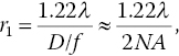
where NA is the numerical aperture of the lens. The approximation holds when NA is small, and the equation is known as the Rayleigh criterion, which specifies the minimum separation between two point sources that may be resolved into two distinct objects.
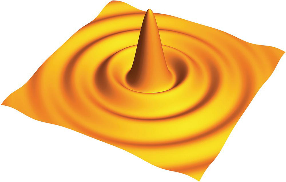
Figure 10.1 An Airy disk resulting from the diffraction of light on a circular aperture.
According to Eq. (10.1), the diffraction barrier (or the resolution limitation) restricts the ability of a microscope to distinguish between two objects separated by a lateral distance of approximately half the wavelength of the light used for imaging. Therefore, to increase the resolution, light with shorter wavelengths (such as ultraviolet and X‐ray) should be used. However, the application often suffers from the lack of image contrast and the risk of radiation damage, making them unsuitable for live cell imaging. To meet the demands for ultra‐sharp resolution, scientists around the world have invested in tremendous amounts of time and effort over the past few decades, and their diligent hard work has led to remarkable progresses, finally breaking the diffraction barrier and bringing optical microscopy to proper use in nanometric dimensions [5–7]. The endeavors were fully recognized in 2014 when the Nobel Prize in Chemistry was awarded to Eric Betzig, Stefan W. Hell, and William E. Moerner “for the development of super‐resolved fluorescence microscopy” [8].
10.2 Superresolution Fluorescence Imaging
10.2.1 Stimulated Emission Depletion Microscopy
A landmark in developing subdiffraction imaging is the stimulated emission depletion (STED) microscopy. The technique involves the use of two laser beams of different wavelengths and shapes [9]. During a STED measurement, the first laser beam (a Gaussian beam) brings the fluorophore of interest to its excited state. The second laser beam, which has a doughnut shape at the focus of the objective lens, depletes the emission from all excited molecules except those in the middle of the doughnut, resulting in a nanometer‐sized volume (Figure 10.2) [10]. Consequently, the final “fluorescent volume” becomes apparently smaller than the diffraction limit of the first laser beam. Naturally, the smaller the fluorescent volume is, the higher the image resolution becomes. Depending on the intensity of the second laser beam (or the STED beam), the fluorescence emission can be confined to a spot with a diameter much smaller than the wavelength of light.
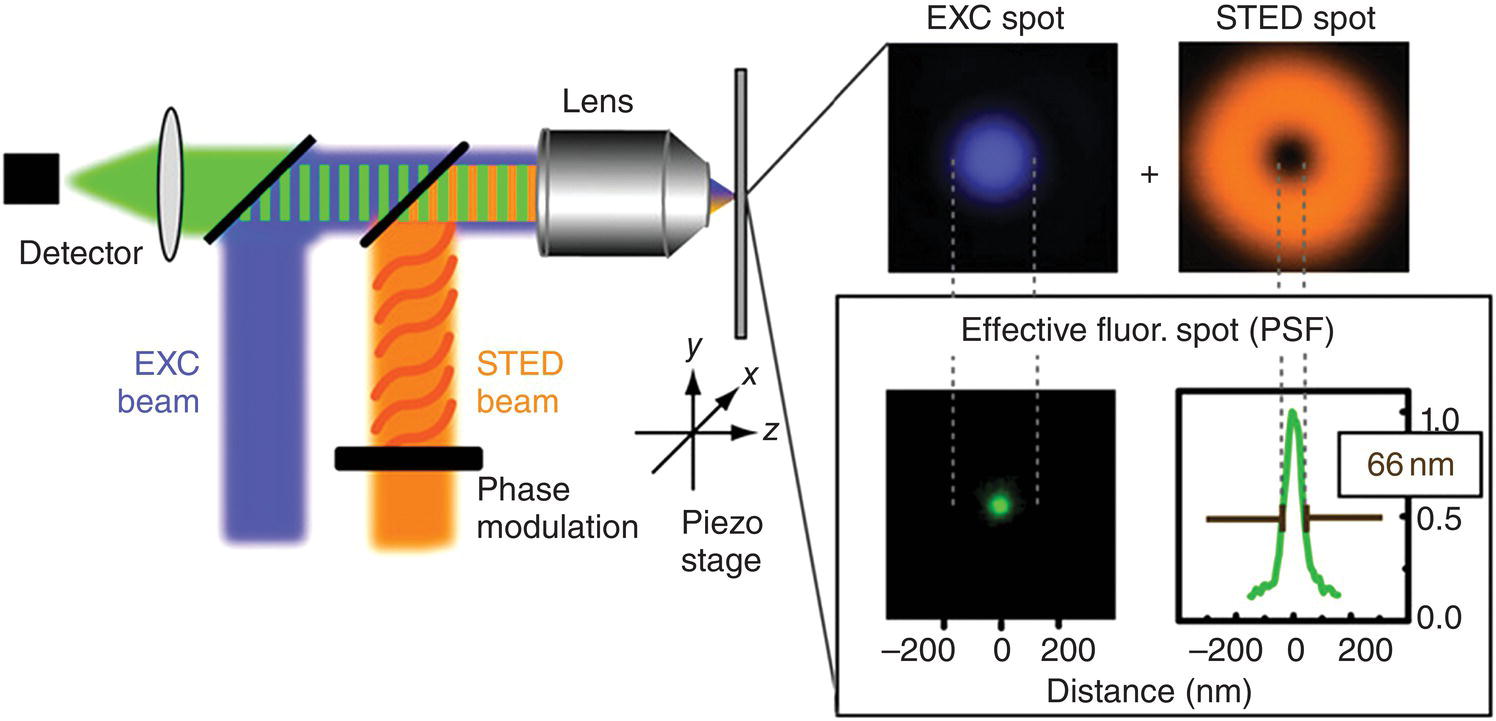
Figure 10.2 Principle of STED microscopy. A blue excitation (EXC) beam is focused to a diffraction‐limited excitation spot, shown in the adjacent panel in blue, while the orange STED beam de‐excites molecules. The STED beam is phase‐modulated to form the focal doughnut shown in the top right panel. Superimposition of the two focal spots confines the area in which emission is only possible in the doughnut center, yielding the effective fluorescent spot of subdiffraction size shown in green in the lower panel.
Source: Adapted with permission from Ref. [10].
Hell and coworkers [11] have shown that in the presence of the STED beam, the Abbe’s equation should be modified to

where n is the refractive index of the medium, I is the laser intensity, and Isat is the saturation intensity at which the probability of the fluorescence emission is reduced by half. STED microscopy is straightforward, requiring no elaborate post‐data processing. In principle, it is the most suitable method for high‐resolution imaging of live cells at real time and in three dimensions. However, due to the fact that the diffraction limit is inversely proportional to the square root of (1 + I/Isat), a STED beam with a high laser power is needed to effectively improve the spatial resolution. For example, using a STED laser power of I = 8Isat will result in only a factor of 3 in resolution improvement. The demand for such a high laser power severely limits the applicability of the method in bioimaging because most molecular fluorophores (such as fluorescein and fluorescent proteins) photobleach rapidly under intense laser illumination. In contrast, the nitrogen‐vacancy (NV−) centers in FNDs are perfectly photostable without photobleaching and blinking, representing one of the few exceptions. Therefore, FNDs are well suited for use as a contrast agent for superresolution imaging by STED microscopy [12–20].
STED was first applied to detect single NV− centers in bulk diamond with a remarkable resolution down to 5.8 nm [12]. Using the same technique (532 nm laser pulses for excitation and 775 nm laser pulses for depletion), Han et al. [13] effectively procured high‐resolution images of 35 nm FNDs spin‐coated on a glass plate, reporting a resolution of 40 nm likely limited by the size of the particles. No photobleaching was found even under STED illumination with a laser power as high as 160 mW. In follow‐up experiments, the research team made further efforts to conduct controlled addressing and readout of the NV− spin states to resolve the individual NV− centers in FNDs. It was demonstrated by Arroyo‐Camejo et al. [14] that the STED microscopy could detect single NV− centers in FNDs with a resolution of 10 nm. Even multiple adjacent NVs located in a single FND could be imaged individually down to a relative distance of 15 nm (Figure 10.3a). These centers were found located predominantly near the center of the particle as confirmed by superimposing images acquired by STED and scanning electron microscopy (Figure 10.3b).
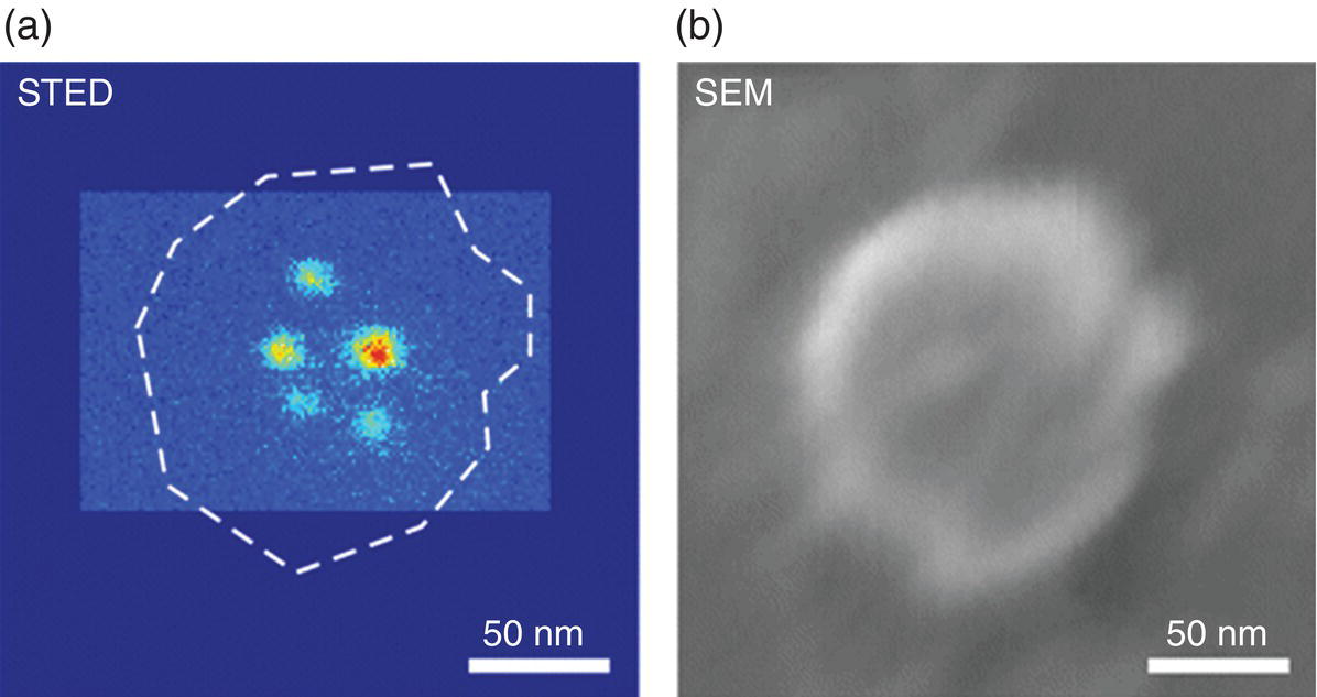
Figure 10.3 (a) STED and (b) SEM images of a single FND particle.
Source: Reprinted with permission from Ref. [14]. Reproduced with permission of American Chemical Society.
Inspired by the success of superresolution imaging of NV− centers, Tzeng et al. [15] applied STED to probe single FNDs in fixed HeLa cells. To prevent particle agglomeration in cell medium, acid‐treated FNDs (~35 nm in diameter) were first noncovalently coated with bovine serum albumin (BSA) and then delivered to the cell cytoplasm by endocytosis (Section 8.1). Using 532‐nm light for excitation and a doughnut‐shaped 740‐nm laser beam for depletion, they attained a spatial resolution of approximately 40 nm (cf., captions in Figure 10.4 for details). The resolution allowed for the identification of single isolated FND particles in cells and distinguished them from FND aggregates confined in the endosomes. The study provided new insight into the FND uptake mechanism of cells, as discussed in Section 9.1, with single‐particle sensitivity and nanometric resolution. Meanwhile, Prabhakar et al. [16] applied a similar STED technique to probe the endosome merging into late endosomes and estimated the drug load taken up by individual cells with silica‐coated FNDs as the imaging agents as well as the drug carriers. An improvement of the spatial resolution by a factor of 5 was readily achieved by using a high‐power STED laser to deplete the NV− emission. Such improvements in optical imaging are crucial for revealing the detailed structures of biological macromolecular complexes and assemblies, including cellular organelles and subcellular compartments.

Figure 10.4 Confocal and STED imaging of HeLa cells labeled with BSA‐conjugated FNDs by endocytosis. (a) Confocal image acquired by raster scanning of an FND‐labeled cell. The fluorescence image of the entire cell is shown in the white box and demonstrates fairly uniform cell labeling by BSA‐conjugated FNDs. (b) STED image of single BSA‐FND particles enclosed within the green box in (a). (c) Confocal and STED fluorescence intensity profiles of the particle are indicated in (b) with a blue line. Solid curves are best fits to one‐dimensional Gaussian (confocal) or Lorentzian (STED) functions. The corresponding full widths at half‐maximum are given in parentheses.
Source: Reprinted with permission from Ref. [15]. Reproduced with permission of John Wiley & Sons.
In addition to red FNDs, green FNDs containing the N–V–N centers (or H3 in Section 3.3.3) are also amenable to subdiffraction imaging with STED microscopy. Laporte and Psaltis [19] first measured the absorption cross‐section of the H3 centers in green FNDs to be σ = 1.18 × 10⁻¹⁷ cm2 at 470 nm using a saturation method similar to that described in Section 7.1.2 for the NV− centers. Next, STED images were obtained by employing a 488‐nm pulsed laser for excitation and a 590‐nm continuous‐wave laser for depletion. In order to attain high spatial resolution (better than 70 nm), a depletion laser intensity on the order of 100 MW cm−2 was used. The researchers exemplified the application of green FNDs as a non‐photobleaching STED marker by imaging 70‐nm FNDs taken up into HeLa cells. The availability of more than one photostable color centers of FNDs has opened a door to perform multicolor imaging and spatial correlation studies with STED.
While green and red FNDs show great potentials, superresolution imaging of them in live cells by STED remains a challenge because the use of a high‐power STED beam often causes photodamage to the target cells. A variation of STED is ground‐state depletion, which requires relatively modest laser intensity (1 MW cm−2 or less) [21]. Hell and Kroug [22] first proposed in 1995 that if the doughnut‐shaped depletion beam could excite the fluorophores to a long‐lived dark state, i.e. a state where little or no fluorescence occurs, images with high resolution could also be obtained. Applying the same principle and taking advantage of the photochromic properties of NV centers (Figure 3.7), Chen et al. [23, 24] developed a technique known as charge‐state depletion microscopy to achieve superresolution. Specifically, two pulsed laser beams (637 and 532 nm) were used to initialize and switch the charge states, and the third pulsed laser (589 nm) detected the NV− centers. The experiment started with the photoionization of nearly all NV− centers to form NV0 with the 637‐nm Gaussian laser beam, only to be followed by a 532‐nm doughnut‐shaped laser beam for the photoconversion of NV0 to NV−, which was finally detected with the 589‐nm light. The researchers were able to resolve the individual NV centers in bulk diamond with a resolution as fine as 4.1 nm, where the centers appeared as dark spots in the fluorescence image. In practical bioimaging, it is preferable to have the fluorophores appearing as bright spots, instead of dark spots. This was achievable by changing the roles of the 637‐ and 532‐nm laser beams at the expense of resolution. Despite that the resolution was significantly reduced to 28.6 nm, the imaging required the use of lasers with a power density on the order of 1 MW cm−2, which represented a factor of 100 lower than that used in STED to achieve comparable resolution. The technique makes it possible to perform superresolution imaging of FNDs in live cells.
Finally, FNDs have been applied as photostable nanoprobes to compare the performance between STED microscopy and structured illumination microscopy (SIM), which is another useful technique to achieve superresolution imaging [25]. Side‐by‐side comparison of the resolution of these two methods with 35‐nm FNDs at the single particle level showed that STED provided more structural details, whereas SIM offered a larger field of view with a higher imaging speed [18]. However, SIM tended to produce deconvolution smoothing and orientational artifacts due to the post‐data processing. In a separate study, FNDs were also employed to investigate the polarization effects in lattice‐STED microscopy, where superresolution imaging with 75‐nm resolution and a field of view of 7.5 μm × 7.5 μm was achieved [20]. Notably, the exceptional photostability of the particles made it possible to image 35‐nm FNDs at different optical lattice configurations and compare the experimental measurements with theoretical simulations.
10.2.2 Saturated Excitation Fluorescence Microscopy
In conventional fluorescence microscopy, the instrument is typically operated in the linear mode, namely, the measured fluorescence intensity is linearly proportional to the excitation energy. However, saturation may occur if the excitation intensity elevates while the number of molecules in the excitation volume stays the same. This nonlinear effect is more prominent in the center than at the edge of the laser focus as the intensity distribution is Airy‐like as illustrated in Figure 10.1. One can thus improve the spatial resolution if the nonlinear components in the fluorescence intensity distribution are extracted for imaging. The concept can be realized by temporally modulating the excitation laser intensity at a frequency (ω) and demodulating the measured fluorescence intensity at the corresponding harmonic frequencies (i.e. 2ω, 3ω, …), where the signals are produced due to the nonlinear effect. Theoretical simulations show that high harmonic fluorescence signals contribute most to the resolution improvement and a higher resolution is attained at a higher demodulation frequency (Figure 10.5) [26]. Approximately a twofold improvement is achievable in both lateral and axial directions, if the eighth harmonic signals are detected for imaging.

Figure 10.5 Fluorescence intensity profiles on the lateral (x) and axial (z) axes, calculated for different demodulation frequencies in saturated excitation fluorescence microscopy. The excitation intensities used to obtain the demodulated intensity profiles at ω, 2ω, 4ω, and 8ω are 1.5, 15, 400, and 700 kW cm−2, respectively.
Source: Reprinted with permission from Ref. [26]. Reproduced with permission of American Physical Society.
An intrinsic difficulty associated with this so‐called saturated excitation fluorescence microscopy is that it requires high illumination intensities to saturate fluorophores in the excited states. Similar to STED, the high laser intensities often result in rapid photobleaching. Fujita and coworkers [27] utilized FNDs as photostable fluorescent nanoprobes to circumvent this problem. They confirmed that FNDs exhibited a nonlinear fluorescence response under the saturated excitation conditions generated by intense laser light. A lateral resolution of 140 nm could be achieved at the demodulation frequency 4ω and a laser intensity of 25 kW cm−2. The exceptionally high photostability of FNDs allowed the researchers to quantify the spatial resolution improvement inherent in this method and demonstrate the scalability of the spatial resolution of this nonlinear superresolution method. The use of FNDs also enabled the research team to perform fluorescence imaging of multicolor‐stained macrophage cells with a spatial resolution beyond the diffraction limit.
10.2.3 Deterministic Emitter Switch Microscopy
The capability of detecting single NV− spins in FNDs by optically detected magnetic resonance (ODMR) offers a different route to superresolution imaging. The fundamental principle behind this method is that the degeneracy of the ms = ±1 sublevels at the ground state of NV− is lifted in the presence of a magnetic field via the Zeeman effect (Figure 10.6a), and the energy difference between these two sublevels depends on the strength of the applied magnetic field as well as the orientation of the magnetic moment of the NV− center with respect to the field. In bulk diamond, the NV− center has four possible orientations and thus four distinct Zeeman splittings (Figure 10.6b and c). If only one pair of the spin resonance peaks is observed in the ODMR spectrum, it is an indication for the presence of a single NV− center in the laser probe volume (cf., Figure 3.9). This unique magneto‐optical property makes it possible to achieve superresolution of differently oriented centers by multispectral imaging in the microwave domain. Dolde et al. [28] have demonstrated the principle by exploiting the spin addressability for subdiffraction microscopy of two NV− centers in bulk diamond. Compared with single‐spin stochastic optical reconstruction microscopy (STORM) [29], which utilizes a low‐power 594 nm laser to induce frequent switching between NV− and NV0 centers, the ODMR method is deterministic and more straightforward, requiring less post‐data processing.

Figure 10.6 (a) Energy level diagram of NV−, showing how preferential shelving of the ms = ± excited states (3E) into the dark metastable state (1A) gives rise to a typical electron spin resonance spectrum. (b) Fluorescence of two NV− centers in the presence of a static magnetic field as a function of applied microwave frequency. The splitting of the two dips (ΔωA and ΔωB) is given by the projection of the incident magnetic field on the magnetic moment of the NV−. The contrast of each dip has an inverted Lorentzian shape. (c) Illustration of NV− centers in a static magnetic field, each having field splitting frequencies corresponding to their uniquely oriented magnetic moments relative to the magnetic field. (d) Schematic diagram of the method for resolving a switchable emitter by taking the difference between two images where a uniquely addressed emitter is dimmed and not dimmed by resonant microwave excitation at I(ΩZFS ± Δω) and I(Ωo), respectively. ZPL, zero‐phonon line; ZFS, zero‐field splitting.
Source: Adapted with permission from Ref. [30]. Reproduced with permission of American Physical Society.
With random orientation on a substrate, FNDs, in principle, have an unlimited number of NV− centers that may be distinguishably addressed with this ODMR‐based superresolution imaging technique. However, in reality, the number is limited by the width of the spin resonance peaks. On the basis of the peak width (typically 20 MHz) and the field‐dependent peak shift (~28 MHz mT−1), Chen et al. [30] estimated that at an applied magnetic field of 20 mT in strength, it is possible to resolve more than 50 uniquely addressable NV− centers within a diffraction‐limited spot. However, instead of conducting experiments in confocal mode, a technique called wide‐field deterministic emitter switch microscopy was developed to achieve high‐speed, subdiffraction imaging with low laser intensities across a wide field of view. Under resonant microwave excitation, only the NV− centers with correct orientation showed a reduction in fluorescence intensities and could be clearly identified by subtraction of the signals with and without the presence of the resonant microwave excitation (Figure 10.6d). By using this technique, the research team was able to resolve two FNDs, each containing a single NV− center, physically separated by 55 nm apart and determine their locations down to 12‐nm precision over a wide area of 35 × 35 μm2.
10.2.4 Tip‐Enhanced Fluorescence Microscopy
The diffraction barrier, i.e. Eq. (10.3), exists when the diffraction pattern is viewed at the focal plane of a converging lens or when it is viewed at a long distance from the aperture, known as the far field [1]. Various near‐field techniques have been developed to extend optical microscopy beyond the diffraction limit [31]. The introduction of an aperture probe to enable near‐field imaging, known as near‐field scanning optical microscopy, has proven to be a successful approach [32, 33]; however, the low light throughput from the probe (~10−4 for a 100 nm aperture), together with some practical complications in the implementation, prevents widespread use of the technique. To overcome these limitations, researchers in the field have invented an alternative method by replacing the aperture probe with a sharp metal tip to achieve far‐field superresolution fluorescence imaging [34].
A metal tip is known to enhance both Raman and fluorescence signals due to plasmon oscillation at the tip [35]. Plasmon oscillation is a collective response of electrons, which can produce a highly localized electric field that in turn can accelerate the radiative and non‐radiative decay rates of nearby fluorophores. The field enhancement is so tightly confined to the vicinity of the tip apex that the method is applicable to improve the optical resolution to below the diffraction limit of light. The applicability of the tip‐enhance fluorescence microscopy was first demonstrated with dye molecules [34] and quantum dots [36, 37], achieving a spatial resolution in the range of 20 nm.
Hui et al. [38] extended the study to FNDs at the single particle level by applying radially polarized light to excite the plasmon oscillation of the gold tip of an atomic force microscope (AFM). With FNDs of approximately 30 nm in diameter (Figure 10.7a) and an experimental setup similar to that displayed in Figure 7.4a, their work showed that the gold tip increased not only the fluorescence intensity of the NV− centers in FNDs but also the optical resolution of the fluorescence image of the particles down to 40 nm (Figure 10.7b and c). An average fluorescence intensity enhancement by a factor of three could be achieved when the tip was placed in close contact with the particle. From a measurement of the fluorescence decay lifetime and the saturation intensity, it was confirmed that the fluorescence enhancement was contributed predominantly by an increase of the radiative decay rate. Using a similar setup, Beams et al. [39] also investigated the near‐field optical properties of FNDs and found that the NV− centers in the particles could serve as a sensitive probe of the surrounding electromagnetic mode structure. Equipped with the enhanced sensitivity, the research team attained the local density of states for an optical antenna by fluorescence lifetime imaging of the single NV− centers.
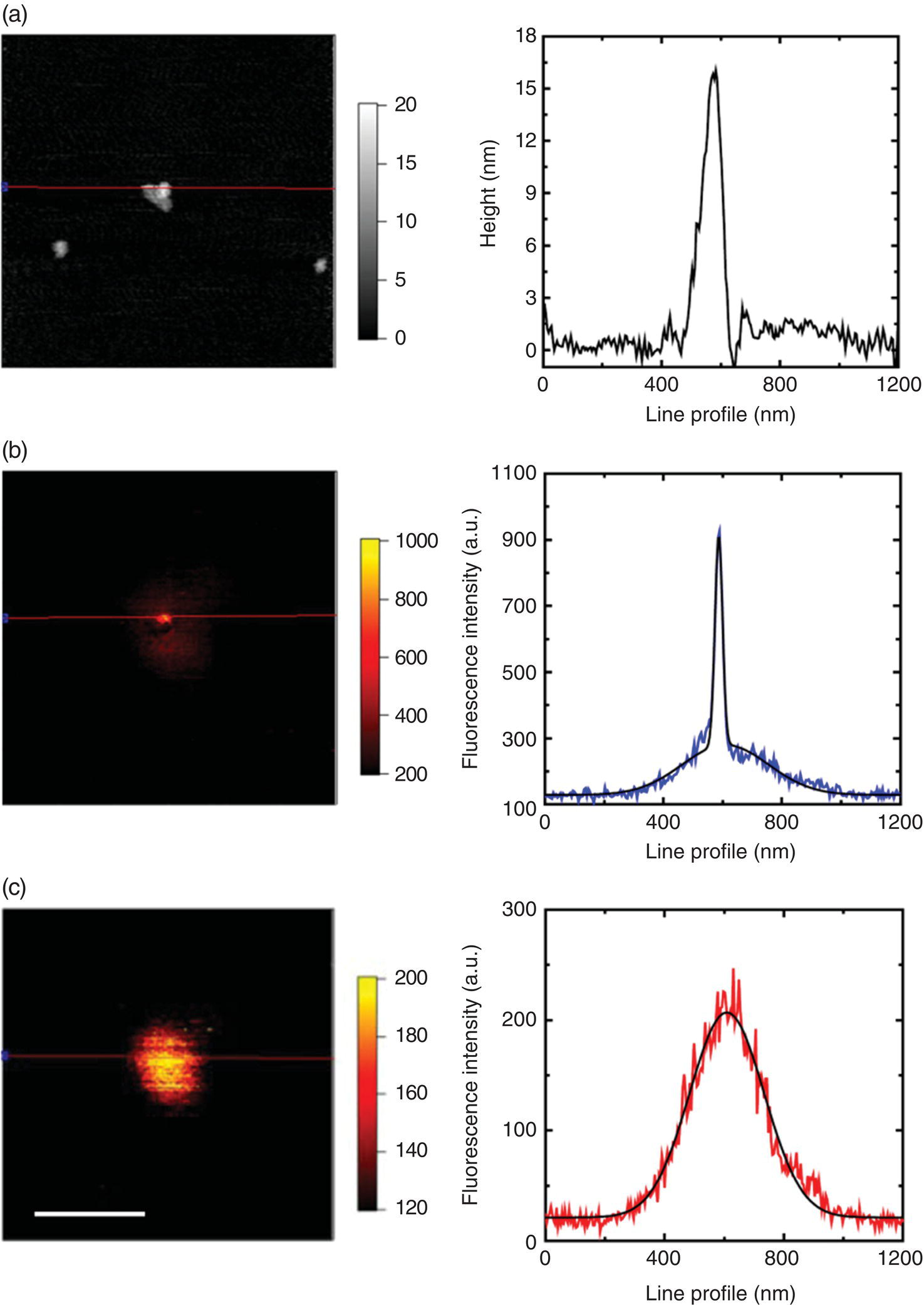
Figure 10.7 (a) AFM image, (b, c) fluorescence images, and their corresponding line profiles of a 30‐nm FND particle (b) with and (c) without a gold tip close to it. The resolution of the fluorescence image is significantly improved by the tip enhancement effect from (c) 290 nm to (b) 40 nm. The gray scale in (a) is in unit of nm. Black solid curves are best Gaussian fits to the experimental data. Scale bar: 400 nm.
Source: Adapted with permission from Ref. [38]. Reproduced with permission of AIP Publishing LLC.
10.3 Cathodoluminescence Imaging
CL is the emission of photons when an electron strikes a luminescent material. It is a tool commonly used to characterize materials with nanometric resolution based on their dispersed fluorescence spectra. Consider an electron beam of 20 keV in energy. The wavelength of the electrons in the beam is λ = 27 pm, according to the de Broglie equation [40],
where h is the Planck constant, m is the mass of an electron, v is the velocity, e is the charge, and V is the acceleration voltage. This calculated wavelength is much smaller than that of visible photons (λ = 400–800 nm) and thus capable of resolving features that cannot be visualized by optical microscopy. The resolution of an electron microscope is theoretically unlimited, depending only on the energy of the electrons. In a standard scanning electron microscope (SEM), which typically operates in the energy range of 1–40 keV, the attainable resolution is on the order of a few tens of nanometers, whereas when using a transmission electron microscope (TEM), which typically operates in the energy range of 100–400 keV, nanometer‐sized structures can be readily resolved.
A CL microscope typically consists of an SEM, a light collection system, and a fluorescence spectrometer [41]. By scanning the electron beam and analyzing the light emitted at each point, similar to the mode used in laser scanning confocal fluorescence microscopy, a map of the optical activity of the specimen can be obtained. However, unlike optical photons, the electron beam often causes destruction of the biological samples under examination, leading to low intensity and rapid degradation of the signals of the fluorescent labels. A possible solution to this problem is to use robust nanoparticles containing photostable and spectrally distinct fluorophores as the biolabels. FND is among the few nanoparticles that can meet the stringent requirements. Using FNDs, Glenn et al. [42] demonstrated the value of red FNDs for CL imaging by acquiring well‐correlated CL and secondary electron images of the individual FND particles in the size range of 40–80 nm. Much superior to fluorescence imaging, the CL microscopy provided a spatial resolution in the region of 5 nm, surpassing the diffraction limit of light. Similarly, Kociak and coworkers [43–45] studied the spectrally and spatially resolved CL of FNDs using a focused electron beam equipped in a scanning transmission electron microscope (STEM). They were able to identify different color centers, including H3 and NV0, in a mixture of green and red FND particles (Figure 10.8a and b) through careful analysis of the CL spectra (Figure 10.8c and d) [44]. Their work verified the feasibility of STEM for ultrahigh‐resolution CL imaging of multicolor centers in FNDs. In all these studies, no CL was observed from NV−, probably due to the charge state conversion of the centers from NV− to NV0 during electron irradiation.
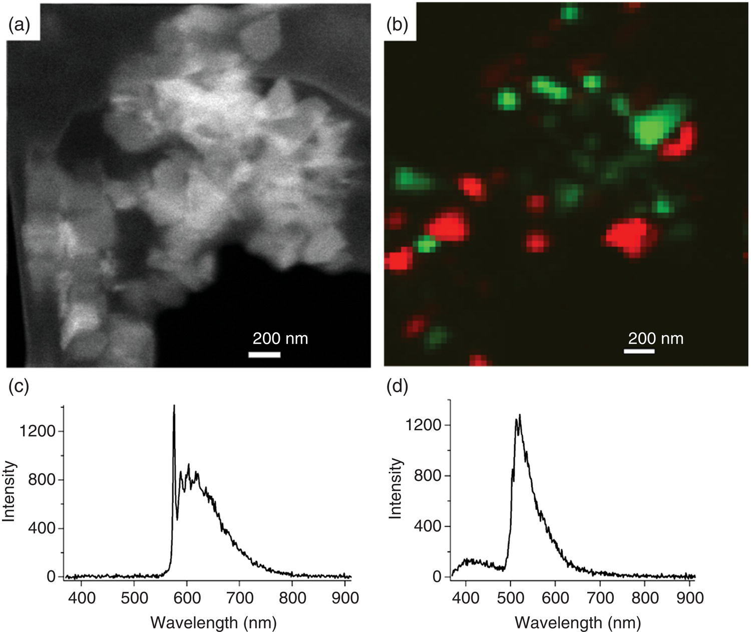
Figure 10.8 (a) STEM image of a FND mixture. (b) Color‐coded intensity map of NV0 (red) and H3 (green) centers in the FNDs. (c, d) Typical CL spectra of FNDs containing NV0 and H3 centers in (c) and (d), respectively.
Source: Reprinted with permission from Ref. [44]. Reproduced with permission of John Wiley & Sons.
In a separate study, high spatial resolution imaging of FNDs in live cells was performed with a technique called direct electron beam excitation‐assisted fluorescence microscopy. In this work, Nawa et al. [46] used a focused electron beam to excite both green and red FNDs in HeLa cells cultured on a silicon nitride membrane attached to an SEM. Similar to atmospheric scanning electron microscopy [47], the electron beam emitting from the SEM passed through the thin membrane (~50 nm in thickness), irradiated the specimen in solution, and generated CL signals, which were finally collected by an optical microscope for detection. Two‐color imaging demonstrated that these two different types of FNDs could be simultaneously observed within the same cells with nanometer resolution (cf., captions in Figure 10.9 for details). The technique is potentially applicable for multicolor immunostaining after proper conjugation of FNDs with antibodies to elucidate various cellular functions (Section 4.2). By using the bioconjugated FNDs along with these new methods, researchers have been able to achieve molecular localization and, simultaneously, reveal the structural details of cellular organelles with STEM [48].

Figure 10.9 Images of both green and red FNDs internalized in HeLa cells, acquired with (a) phase contrast microscopy and (b) direct electron beam excitation‐assisted (D‐EXA) fluorescence microscopy. The magnified D‐EXA image of the area marked with a red square in (c) shows a spatial resolution of 155 nm in (d).
Source: Reprinted with permission from Ref. [46]. Reproduced with permission of John Wiley & Sons.
10.4 Correlative Light‐Electron Microscopy
CLEM is a technique recently developed to analyze the same specimen with both light microscopy (LM) and electron microscopy (EM) [49]. It combines the advantages of the multicolor versatility of LM with the high‐resolution power of EM for molecular and cellular biology research. However, different from CL, CLEM images are acquired with two entirely different instruments and therefore colocalization of the same objects at the micrometer or even nanometer scale is crucial. A number of nanomaterials have been developed as fluorescent fiducial markers for CLEM, including dye‐labeled nanogolds, dye‐doped polystyrene beads, and quantum dots [50]. However, these nanomaterials are not sufficiently stable to allow routine CLEM analysis because, in order to avoid damaging the markers during sample preparation, the specimens must be fixed by high‐pressure freezing, which is a highly specialized technique and a time‐consuming process. Moreover, the correlative analysis cannot be repeatedly carried out due to fluorescence quenching of these markers by heavy metal staining with reagents, such as OsO4 and uranyl acetate, required for EM imaging. The use of CLEM for nanometric localization of biological molecules in cells remains a challenge, despite that some successful cases have been reported in the literature [51].
For any molecule or material to serve as a good fluorescent fiducial marker for CLEM, the prerequisites are: highly fluorescent and electron‐dense. FND is appealing for this application because the nanomaterial has both high light‐emitting capability and a dense carbon core that can be visualized by EM [52–57]. In addition, the detection of the nanomaterial by LM imaging is highly compatible with the post‐embedding technique, which involves staining of the specimens with heavy metals for structural preservation in EM. The high compatibility stems from the fact that the fluorescent centers of FNDs are so deeply buried inside the diamond matrix that their fluorescence properties can hardly be altered by the environmental changes (Section 6.2). An added benefit is that background‐free detection of FNDs on the grids and in the sections can be achieved by time‐gated fluorescence imaging (Section 8.2.4). Therefore, reliable co‐registration of LM and EM images is both possible and practical with FNDs as the fluorescent fiducial markers.
An application of CLEM to image and localize the positions of antigens on cell surface was first made by Hsieh et al. [56] using lipid‐encapsulated FNDs. The researchers encapsulated surface‐oxidized FNDs in lipids, followed by grafting of the lipid layers with biotin molecules (Section 4.3.1). The biotinylated lipid‐coated FNDs (bL‐FNDs) were then used to target the surface antigen CD44 on HeLa cells by sandwich immunostaining (Section 8.1.2). Figure 10.10a shows a SEM image of HeLa cells labeled with bL‐FNDs. Clearly, the SEM image provided considerably more structural information than the corresponding LM images. Despite that some bL‐FNDs could be identified under high magnification (Figure 10.10b and c), it was still challenging to unambiguously differentiate bL‐FNDs from the complex nanostructures on the cell surface. Taking advantage of the exceptionally high chemical and photophysical stability of FNDs as detailed earlier, the research team was able to detect their fluorescence readily even after strong irradiation of the Pt‐coated cell samples with 10‐kV electrons in SEM (Figure 10.10d and e). By superimposing the LM and EM images with one of them tilted by a certain angle, the locations of the CD44 antigens on the HeLa cell membrane could be determined with an accuracy of 50 nm, which is about 1/5 that of the diffraction limit of light (Figure 10.10f–i).

Figure 10.10 (a) SEM images of a HeLa cell labeled with anti‐CD44 antibody, neutravidin, and bL‐FND. (b–g) Enlarged views of (b, c) SEM images, (d, e) fluorescence images, and (f, g) CLEM images of the white boxes in (a). The tilt angles to achieve complete overlaps of the FNDs are 39° and 1° for (b, d) and (c, e), respectively. (h) Intensity profiles of the white dashed line drawn in panel (i), which is an enlarged view of the white box in (g). Scale bars: 10 μm in (a) and 2 μm in (b, c).
Source: Adapted with permission from Ref. [56].
Apart from SEM, the FND‐labeling technique is also compatible with TEM. Figure 10.11a–c displays TEM images of HeLa cells without and with labeling. Many single isolated FNDs were found on the cell surface. To obtain LM images for the same specimen after TEM imaging, the fluorescence signals were collected with a delay time of more than 3 ns after pulsed laser excitation to reduce the background signals arising from the plastic‐like resins, in which the samples were embedded. Using this time‐gating technique, the researchers were able to identify clearly the individual 100‐nm FND particles on the surface of the cells in the thin‐sectioned resins. More importantly, the EM image (Figure 10.11d) and the time‐gated LM image (Figure 10.11e) were literally superimposed with each other (Figure 10.11f). Up to 30 particles showed excellent co‐registration between these two images when the fluorescence image was tilted by 17°. The high brightness and superior photostability of the particles enabled the positions of the CD44 antigens to be located with an accuracy of better than 50 nm, limited mainly by the size of the FND particles. This combined LM and EM analysis, along with the use of smaller FNDs, has opened the door to locate the positions of antigens on cell surface with unprecedented precision and accuracy.
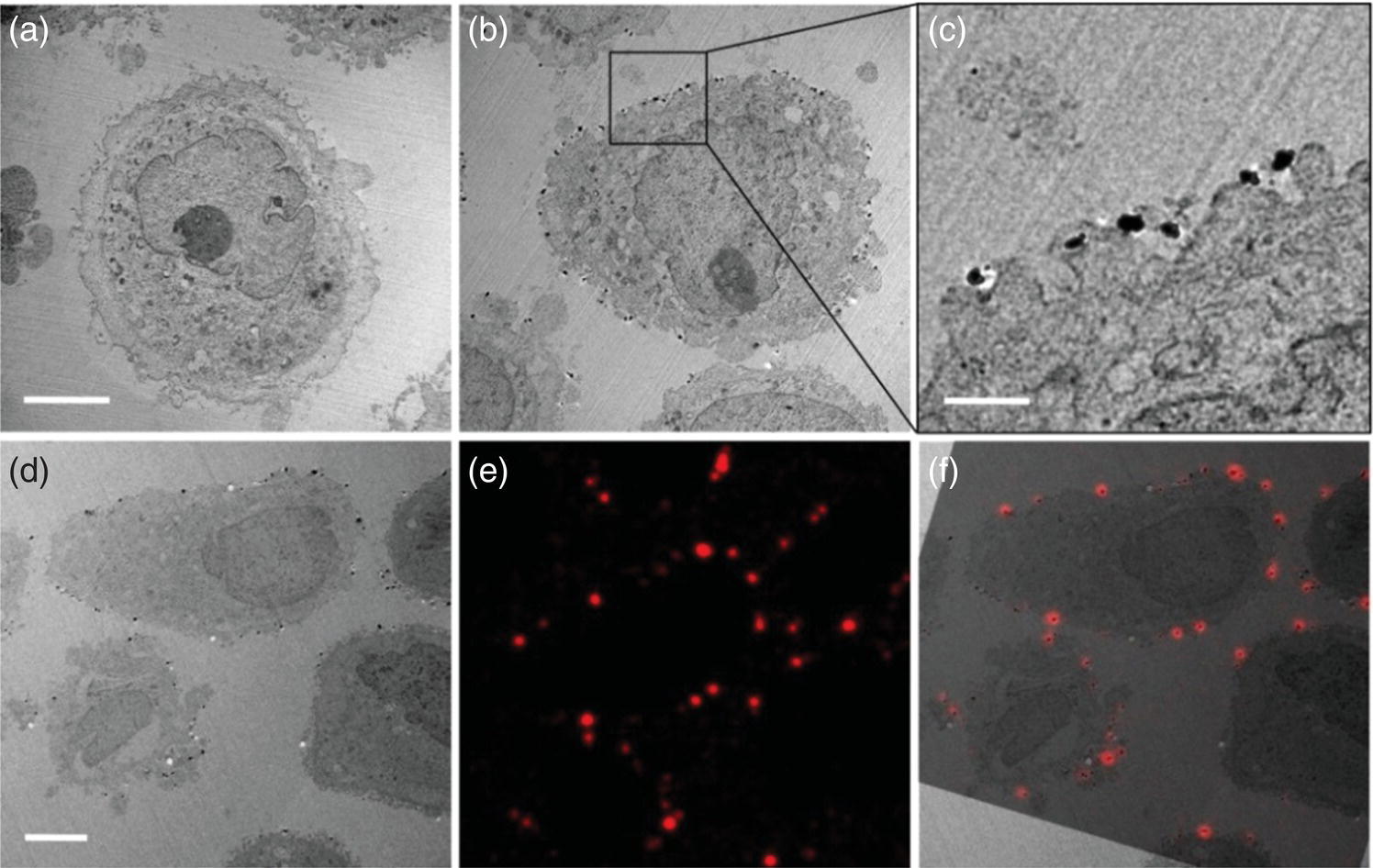
Figure 10.11 (a) TEM image of suspended HeLa cells without labeling. (b–d) TEM images of suspended HeLa cells labeled with biotin‐anti‐CD44 antibody, neutravidin, and then biotinylated lipid‐coated FND. (e, f) Fluorescence and CLEM images of the same sample in (d). The electron energy used to obtain the TEM images is 120 kV. Scale bars: 5 μm in (a, d) and 1 μm in (c).
References
- 1 Lauterbach, M.A. (2012). Finding, defining and breaking the diffraction barrier in microscopy – a historical perspective. Opt Nanoscopy 1: 8.
- 2 Abbe, E. (1873). Beiträge zur Theorie des Mikroskops und der mikroskopischen Wahrnehmung. M. Schultze’s. Archiv für mikroskopische Anatomie 9: 413–468.
- 3 Fowles, G.R. (1989). Introduction to Modern Optics, 2e. New York: Dover.
- 4 Dullemond, C.P., van Boekel, R. and Quirrenbach, A. (2010). Chapter 3 Diffraction. Observational Astronomy (MKEP5). http://www.ita.uni‐heidelberg.de/~dullemond/lectures/obsastro_2010/Chapter_Diffraction.pdf (accessed 16 April 2018).
- 5 Betzig, E. (2015). Single molecules, cells, and super‐resolution optics (Nobel lecture). Angew Chem Int Ed 54: 8034–8053.
- 6 Hell, S.W. (2015). Nanoscopy with focused light (Nobel lecture). Angew Chem Int Ed 54: 8054–8066.
- 7 Moerner, W.E. (2015). Single‐molecule spectroscopy, imaging, and photocontrol: foundations for super‐resolution microscopy (Nobel lecture). Angew Chem Int Ed 54: 8067–8093.
- 8 The Nobel Prize in Chemistry 2014. Nobelprize.org. Nobel Media AB 2014. https://www.nobelprize.org/nobel_prizes/chemistry/laureates/2014 (accessed 16 April 2018).
- 9 Hell, S.W. and Wichmann, J. (1994). Breaking the diffraction resolution limit by stimulated emission: stimulated‐emission‐depletion fluorescence microscopy. Opt Lett 19: 780–782.
- 10 Willig, K.I., Rizzoli, S.O., Westphal, V. et al. (2006). STED microscopy reveals that synaptotagmin remains clustered after synaptic vesicle exocytosis. Nature 440: 935–939.
- 11 Westphal, V. and Hell, S.W. (2005). Nanoscale resolution in the focal plane of an optical microscope. Phys Rev Lett 94: 143903.
- 12 Rittweger, E., Han, K.Y., Irvine, S.E. et al. (2009). STED microscopy reveals crystal colour centres with nanometric resolution. Nat Photon 3: 144–147.
- 13 Han, K.Y., Willig, K.I., Rittweger, E. et al. (2009). Three‐dimensional stimulated emission depletion microscopy of nitrogen‐vacancy centers in diamond using continuous‐wave light. Nano Lett 9: 3323–3329.
- 14 Arroyo‐Camejo, S., Adam, M.P., Besbes, M. et al. (2013). Stimulated emission depletion microscopy resolves individual nitrogen vacancy centers in diamond nanocrystals. ACS Nano 7: 10912–10919.
- 15 Tzeng, Y.K., Faklaris, O., Chang, B.M. et al. (2011). Superresolution imaging of albumin‐conjugated fluorescent nanodiamonds in cells by stimulated emission depletion. Angew Chem Int Ed 50: 2262–2265.
- 16 Prabhakar, N., Näreoja, T., von Haartman, E. et al. (2013). Core‐shell designs of photoluminescent nanodiamonds with porous silica coatings for bioimaging and drug delivery II: application. Nanoscale 5: 3713–3722.
- 17 Lai, N.D., Faklaris, O., Zheng, D. et al. (2013). Quenching nitrogen‐vacancy center photoluminescence with infrared pulsed laser. New J Phys 15: 033030.
- 18 Yang, X., Tzeng, Y.K., Zhu, Z. et al. (2014). Sub‐diffraction imaging of nitrogen‐vacancy centers in diamond by stimulated emission depletion and structured illumination. RSC Adv 4: 11305–11310.
- 19 Laporte, G. and Psaltis, D. (2015). STED imaging of green fluorescent nanodiamonds containing nitrogen‐vacancy‐nitrogen centers. Biomed Opt Express 7: 34–44.
- 20 Yang, B., Fang, C.Y., Chang, H.C. et al. (2015). Polarization effects in lattice‐STED microscopy. Faraday Discuss 184: 37–49.
- 21 Bretschneider, S., Eggeling, C., and Hell, S.W. (2007). Breaking the diffraction barrier in fluorescence microscopy by optical shelving. Phys Rev Lett 98: 218103.
- 22 Hell, S.W. and Kroug, M. (1995). Ground‐state‐depletion fluorescence microscopy: a concept for breaking the diffraction resolution limit. Appl Phys B Laser Opt 60: 495–497.
- 23 Chen, X., Zou, C., Gong, Z. et al. (2015). Subdiffraction optical manipulation of the charge state of nitrogen vacancy center in diamond. Light Sci Appl 4: e230.
- 24 Chen, X.D., Li, S., Shen, A. et al. (2017). Near‐infrared‐enhanced charge‐state conversion for low‐power optical nanoscopy with nitrogen‐vacancy centers in diamond. Phys Rev Appl 7: 014008.
- 25 Allen, J.R., Ross, S.T., and Davidson, M.W. (2014). Structured illumination microscopy for superresolution. ChemPhysChem 15: 566–576.
- 26 Fujita, K., Kobayashi, M., Kawano, S. et al. (2007). High‐resolution confocal microscopy by saturated excitation of fluorescence. Phys Rev Lett 99: 228105.
- 27 Yamanaka, M., Tzeng, Y.K., Kawano, S. et al. (2011). SAX microscopy with fluorescent nanodiamond probes for high‐resolution fluorescence imaging. Biomed Opt Express 2: 1946–1954.
- 28 Dolde, F., Jakobi, I., Naydenov, B. et al. (2013). Room‐temperature entanglement between single defect spins in diamond. Nat Phys 8: 1–5.
- 29 Pfender, M., Aslam, N., Waldherr, G. et al. (2014). Single‐spin stochastic optical reconstruction microscopy. Proc Natl Acad Sci USA 111: 14669–14674.
- 30 Chen, E.H., Gaathon, O., Trusheim, M.E., and Englund, D. (2013). Wide‐field multispectral super‐resolution imaging using spin‐dependent fluorescence in nanodiamonds. Nano Lett 13: 2073–2077.
- 31 Dunn, R.C. (1999). Near‐field scanning optical microscopy. Chem Rev 99: 2891–2928.
- 32 Pohl, D.W., Denk, W., and Lanz, M. (1984). Optical stethoscopy: image recording with resolution λ/20. Appl Phys Lett 44: 651–653.
- 33 Betzig, E. and Trautman, J.K. (1992). Near‐field optics: microscopy, spectroscopy, and surface modification beyond the diffraction limit. Science 257: 189–195.
- 34 Sanchez, E.J., Novotny, L., and Xie, X.S. (1999). Near‐field fluorescence microscopy based on two‐photon excitation with metal tips. Phys Rev Lett 82: 4014–4017.
- 35 Mauser, N. and Hartschuh, A. (2014). Tip‐enhanced near‐field optical microscopy. Chem Soc Rev 43: 1248–1262.
- 36 Gerton, J.M., Wade, L.A., Lessard, G.A. et al. (2004). Tip‐enhanced fluorescence microscopy at 10 nanometer resolution. Phys Rev Lett 93: 180801.
- 37 Huang, F.M., Festy, F., and Richards, D. (2005). Tip‐enhanced fluorescence imaging of quantum dots. Appl Phys Lett 87: 183101.
- 38 Hui, Y.Y., Lu, Y.C., Su, L.J. et al. (2013). Tip‐enhanced sub‐diffraction fluorescence imaging of nitrogen‐vacancy centers in nanodiamonds. Appl Phys Lett 102: 013102.
- 39 Beams, R., Smith, D., Johnson, T.W. et al. (2013). Nanoscale fluorescence lifetime imaging of an optical antenna with a single diamond NV center. Nano Lett 13: 3807–3811.
- 40 Halliday, D., Walker, J., and Resnick, R. (2010). Fundamentals of Physics, 5e, 993–995. Wiley.
- 41 Yacobi, B.G. and Holt, D.B. (1990). Cathodoluminescence Microscopy of Inorganic Solids. Springer.
- 42 Glenn, D.R., Zhang, H., Kasthuri, N. et al. (2012). Correlative light and electron microscopy using cathodoluminescence from nanoparticles with distinguishable colours. Sci Rep 2: 865.
- 43 Tizei, L.H. and Kociak, M. (2012). Spectrally and spatially resolved cathodoluminescence of nanodiamonds: local variations of the NV0 emission properties. Nanotechnology 23: 175702.
- 44 Tizei, L.H.G., Meuret, S., Nagarajan, S. et al. (2013). Spatially and spectrally resolved cathodoluminescence with fast electrons: a tool for background subtraction in luminescence intensity second‐order correlation measurements applied to subwavelength inhomogeneous diamond nanocrystals. Phys Status Solidi A 210: 2060–2065.
- 45 Meuret, S., Tizei, L.H., Cazimajou, T. et al. (2015). Photon bunching in cathodoluminescence. Phys Rev Lett 114: 197401.
- 46 Nawa, Y., Inami, W., Lin, S. et al. (2014). Multi‐color imaging of fluorescent nanodiamonds in living HeLa cells using direct electron‐beam excitation. ChemPhysChem 15: 721–726.
- 47 Nishiyama, H., Suga, M., Ogura, T. et al. (2010). Atmospheric scanning electron microscope observes cells and tissues in open medium through silicon nitride film. J Struct Biol 169: 438–449.
- 48 Nagarajan, S., Pioche‐Durieu, C., Tizei, L.H. et al. (2016). Simultaneous cathodoluminescence and electron microscopy cytometry of cellular vesicles labeled with fluorescent nanodiamonds. Nanoscale 8: 11588–11594.
- 49 de Boer, P., Hoogenboom, J.P., and Giepmans, B.N. (2015). Correlated light and electron microscopy: ultrastructure lights up. Nat Methods 12: 503–513.
- 50 Kukulski, W., Schorb, M., Welsch, S. et al. (2012). Precise, correlated fluorescence microscopy and electron tomography of lowicryl sections using fluorescent fiducial markers. Meth Cell Biol 111: 235–257.
- 51 Muller‐Reichert, T. and Verkade, P. (ed.) (2102). Correlative Light and Electron Microscopy. Elsevier Science.
- 52 Zurbuchen, M.A., Lake, M.P., Kohan, S.A. et al. (2013). Nanodiamond landmarks for subcellular multimodal optical and electron imaging. Sci Rep 3: 2668.
- 53 Lake, M.P. and Bouchard, L.S. (2017). Targeted nanodiamonds for identification of subcellular protein assemblies in mammalian cells. PLoS One 12: e0179295.
- 54 Hemelaar, S.R., de Boer, P., Chipaux, M. et al. (2017). Nanodiamonds as multi‐purpose labels for microscopy. Sci Rep 7: 720.
- 55 Prabhakar, N., Peurla, M., Koho, S. et al. (2018). STED‐TEM correlative microscopy leveraging nanodiamonds as intracellular dual‐contrast markers. Small 14: 1701807.
- 56 Hsieh, F.J., Chen, Y.W., Huang, Y.K. et al. (2018). Correlative light‐electron microscopy of lipid‐encapsulated fluorescent nanodiamonds for nanometric localization of cell surface antigens. Anal Chem 90: 1566–1571.
- 57 Sotoma, S., Hsieh, F.J., Chen, Y.W. et al. (2018). Highly stable lipid‐encapsulation of fluorescent nanodiamonds for bioimaging applications. Chem Commun 54: 1000–1003.