1
Introduction to Nanotechnology
In his 2017 budget request to the US Congress, President Obama included $1.4 billion for the National Nanotechnology Initiative (NNI), an overarching program coordinating some 20 federal agencies and departments in all activities of nanotechnology R&D, policies, and regulation [1]. For the same time period, President Obama’s budget for the entire National Science Foundation (NSF) was $7.964 billion, a 6.7% increase from the previous year’s, which would cover the vast majority of research programs in all areas of science in the United States, including a $400 million contribution to the NNI’s budget [2], a share of about 18% of the NSF’s budget. All combined, the United States alone has invested nearly $24 billion since the inception of NNI in 2001 with its annual budget tripled during the same period of time. Today, similar national nanotechnology programs exist in more than 60 countries worldwide. At the other end, the global market for nanotechnology products was reported to be about $26 billion in 2014 alone, an impressive growth from the previous year’s $23 billion, and was predicted to reach $62 billion by 2019 based on a compound annual growth rate of 19.8% [3]. With such a vast investment worldwide and a double‐digit annual growth rate in its global gross revenue, nanotechnology has been coined as the technology of the twenty‐first century. Yet, the century is still young and so is the nanotechnology industry.
So, how was it all started? What have happened to nanotechnology throughout the years? And, where are we now? We will survey the now and then in the development of nanotechnology in this chapter, with specific interest in the fields of nanocarbons, paving the way to further discussions of nanodiamonds and fluorescent nanodiamonds in the following chapters.
1.1 Nanotechnology: From Large to Small
1.1.1 Feynman: Plenty of Room at the Bottom
Nanotechnology, a term first adopted by Norio Taniguchi of Tokyo University of Science in 1974 to describe the thin film deposition in his semiconductor processing work [4], is defined by NNI as “science, engineering, and technology conducted at the nanoscale, which is about 1 to 100 nanometers.” Building from the small size, nanotechnology has developed across a wide open landscape in science and engineering, including physics, chemistry, biology, materials science, and many other hybrid new fields. Despite all its blooming development, the original ideas of nanoscience and nanotechnology can be traced back to Richard Feynman’s speech at Caltech in 1959 on his vision of miniaturization in materials [5]. After half a century now, the tiny world that Feynman so vividly painted in his speech is becoming ever more realistic than the world we presently live in with plenty more development still to come.
Feynman gave his first views on nanotechnology over a talk entitled “There’s Plenty of Room at the Bottom” on 29 December 1959 at the annual meeting of the American Physical Society. In this talk, as anyone would have done in promoting a new product, Feynman tried to address the fundamental questions in this new field like: Why making things small? Can it be done? If so, how? What good will come out of things being small? Where and how to use it, including models, examples, challenges, etc.? Feynman first used an illustration of writing an entire 24 densely packed volumes of the Encyclopedia Britannica on a head of a pin to describe his ideas of being small. Making any material in such a small size was neither perceivable nor imaginable at that time. If we were present at Feynman’s talk, in retrospect, we would have witnessed that there were less than 2000 computers in the United States and each IBM computer could take up more than a floor’s space and, with accessories and service facilities, could easily occupy an entire building. We would also see the first ever moon landing by a no‐man spacecraft, Luna 2, and the invention of the first laser by Theodore Maiman and the first appearance of COBOL, a high‐level business‐oriented computer language dominating throughout the rest of the twentieth century and into the beginning of the new millennium. As for our financial investment, Hewlett‐Packard stock was only just accepted by New York Stock Exchange for trading and the first integrated circuit chip was sold for a $120 market price. Looking back, Feynman’s idea of “manipulating and controlling things on a small scale” was both revolutionary and largely fictional under such environment. No doubt, there was a lot of convincing to do in this speech.
But, first, why? Why make things small? How small is small?
Feynman answered the questions right from the beginning of his talk in his own words: it is precisely because “enormous amounts of information can be carried in an exceedingly small space.” For example, if we were to use some 100 atoms (e.g. a 5 × 5 × 5 cube of metal atoms) for one “bit” of information, we could store the information of all 24 million volumes of books that the world had accumulated up to 1959 in a metal cube of 1/200 of an inch wide, a tiny dust barely visible by human eyes. In addition to storing massive information in a small space, we want nanomaterials to work for us. Feynman used cellular biosystems as a model for all man‐made nanomaterials to follow. These nanomaterials, for example, should be small in size, active, mobile, and each one has its own specific functions. Moreover, they must be able to manipulate themselves so as to transmit information from one onto another, again, like that occurring in biosystems, not simply to store information. Imagine the possibilities, if we would just stop for a moment and look around, what it could do for us once we learn how to manufacture nanomaterials: from personal health care to agriculture, construction, communication, and explorations in new frontiers both on our earth and in outer space.
There will be plenty of good things coming from making things on such small scale. The most significant improvement is, perhaps, the speed. Using computer‐aided facial recognition as an example, Feynman quickly pointed out that with all necessary materials and powers available at his present time, a computer of the size of Pentagon would have been needed to complete the task and it would have taken an impatiently long time to process the information. Furthermore, “because of its large size, there is finite time required to get the information from one place to another.” After all, the information transfer cannot go faster than the speed of light. Even half a century ago, Feynman was correct to predict that “when our computers get faster and faster and more and more elaborate, we will have to make them smaller and smaller.” Interestingly, his vision of making smaller computers has been realized in part by today’s state‐of‐the‐art lithography technologies, including electron beam lithography and extreme ultraviolet lithography, to increase the integration density of silicon chips [6].
Taking a daring step forward, Feynman considered bolts and nuts for making small machines and, just for the fun of it, “nanocars.” He looked at the precision in machining, stress and expansion, strength of materials, magnetic force fields, lubrication, heat dissipation, etc., and concluded that with a new design of engine and redesign of the electrical parts, it is possible to make cars on a small scale. He even proposed that one of the ways to use these nanomachines was to perform medical surgery inside our own body. It was a wild idea as he admitted, but little did he know that similar concepts are also being implemented 50 years later today to develop nano‐carriers for drug delivery.
As with any initiatives, Feynman acknowledged challenges and obstacles existing along the way. The first and foremost one was the electron microscope, which was capable of resolving only 10 Å, the very best at the time. In order to carry out the work described in his speech, Feynman would need electron microscopes improved by at least 100 times in resolving power. Consequently, he made a public plea in this speech both to his audience in the meeting and the physics community at large for redesigning new high‐power electron microscopes. It was not until 20 years later when Gerd Binnig and Heinrich Rohrer invented the scanning tunneling microscope (STM) in 1982 [7] and the atomic force microscope (AFM) in 1986 [8] before Feynman’s death in 1988. The invention of both STM and AFM, together with the design of the first electron microscope by Ernst Ruska, was recognized by the Nobel Prize in Physics 1986 [9]. These three types of microscopes have become standard instruments today in the studies of nanoscience and nanotechnology.
A wonderful inspiration as Feynman’s speech was, it did not cause an immediate rush in the science community to make nanoscale materials, mainly because of the lack of appropriate tools (and, perhaps equally deficient, the knowledge of making) at the time. Nevertheless, the significance of Feynman’s vision precipitated gradually throughout time and today anyone who studies the history of nanoscience and nanotechnology will regard this speech a milestone marking the birth of a new field. The field, which affects every aspect of human life from electronics, energy, medicine, and cosmetics, to food and agriculture, virtually writes a new page in human civilization. As our historian friends would be happy to remind us, history and civilization are frequently made by circumstantial occasions and incidents, which might be as simple as a speech. It may even not necessarily be a large audience or the speaker may not be aware at the time of the prevailing outcome that would follow in the long years. Mark Antony’s “Friends, Romans, countrymen, lend me your ears” in replying to Marcus Brutus’s assassination of Julius Caesar, Abraham Lincoln’s “The Gettysburg Address,” and Martin Luther King’s “I have a dream” are few examples of well‐known speeches that had profound impacts on the course of human history. Now, we add Feynman’s speech to this list.
1.1.2 Nanotechnology Today
Not until mid‐1980s, when STM and AFM became available and C60 was discovered [10], did the field of nanoscience and nanotechnology finally receive a long‐awaited boost and set off to a healthy growth by way of developing new nanomaterials as well as new applications. A nice historical timeline is kept current by NNI on its official website [11]. In 2001, recommended by members of his science advisory committee, the US President Bill Clinton inaugurated the NNI involving 20 federal departments, independent agencies, and commissions working together to meet the mission aiming at the creation of “a future in which the ability to understand and control matter at the nanoscale leads to a revolution in technology and industry that benefits society” [12]. NNI is managed by the National Science and Technology Council (NSTC), a cabinet‐level council reporting directly to the US President. The components of federal agencies and departments in NNI include NSF, NIH, NASA, DOE, DOD, EPA, FDA, etc. Therefore, it is a concerted effort across all areas of government institutions to develop a new field that arguably is becoming the signature technology of the twenty‐first century.
In 2008, after two years’ comprehensive work, NNI published a report entitled “Strategy for Nanotechnology‐Related Environmental, Health and Safety Research,” which is the first official EH&S document dealing with nanomaterial management and safety policies in the United States [13]. The document covers five primary categories: (i) instrumentation, metrology, and analytical methods, (ii) nanomaterials and human health, (iii) nanomaterials and the environment, (iv) human and environmental exposure assessment, and (v) risk management methods, which have become the operational standards for nanotechnology industry and research. Five years later, in 2013, the project began its second run of strategic planning and EH&S review and revision, which is still in working progress at the present time. The most exciting current event, perhaps, is the “Nanotechnology‐Inspired Grand Challenge,” launched on 20 October 2015, calling for the scientific community to collaborate in creating “a new type of computer that can proactively interpret and learn from data, solve unfamiliar problems using what it has learned, and operate with the energy efficiency of the human brain” [14]. That is, a humanized computer or an artificial intelligence machine. According to the NNI reports, this Grand Challenge has generated broad interest within the nanotechnology community, including federal and state agencies, and private sectors.
In other parts of the world, on 12 May 2004, the European Commission adopted the communication “Towards a European Strategy for Nanotechnology” [15], which brought the discussion on nanoscience and nanotechnology to an institutional level as an integrated and responsible strategy planning. In the following year, the European Commission adopted the action plan “Nanosciences and Nanotechnologies: An action plan for Europe 2005–2009” [16], which defined a series of articulated and interconnected actions for immediate implementation based on the strategy approved in the previous year. At the same time, the Britain’s Royal Society and the Royal Academy of Engineering published “Nanoscience and Nanotechnologies: Opportunities and Uncertainties” [17], cautioning the risks in the potential health, environmental, social, ethical, and regulatory issues with this new field. The concerns with the general public’s environmental, health, and safety raised in this document may have triggered NNI’s response with a two‐year study and its final 2008 EH&S document, which eventually set the global policies on nanomaterial‐operating protocols and related safety regulations.
1.1.3 The Bottom‐Up Approach
Our discussion so far seems to have focused narrowly on the size miniaturization and, indeed, there are virtues of the size reduction in improving the performance of devices. Personal electronics 3C (computer, communication, and consumer electronics), for example, are getting smaller and smaller each day now and yet they also deliver faster and better quality results ever than before. So, is it that nanotechnology is all about things being small? Though many people may have emphasized over the “nano” part of the technology, this field is far more than the size. It is with the concept of building functional materials and devices from the bottom up. Manufacturing things from the atomic and molecular levels, so‐called nano‐manufacturing, requires carefully designed scale‐up of nanomaterials, devices, and systems. The quality of materials can be greatly enhanced through the processes of nano‐manufacturing, leading to stronger, light‐weighted, durable, and flexible products that, in most cases, also possess unique features to meet their specific needs.
How to manufacture materials from the bottom up? An extreme approach is to design, synthesize, and assemble functional molecules through organic chemistry. A fascinating example in this regard is the synthesis of molecular machines made of parts that are mobile relative to each other. The machines that have been demonstrated to work at the molecular level include a mechanically interlocked architecture consisting of two interlocked macrocycles (known as the catenane), a dumbbell‐shaped molecule threaded through a macrocycle (known as the rotaxane), and a molecular motor consisting of bis‐helicene connected by an alkene double bond [18]. The first nanocar ever built, as envisioned by Feynman in 1959, was made up from oligo(phenylene ethynylene) with alkynyl axles and four spherical C60 wheels as in a conventional car [19]. In recognition of their achievements in molecular nanotechnology, the Nobel Prize in Chemistry 2016 was awarded jointly to Jean‐Pierre Sauvage, Fraser Stoddart, and Bernard Feringa “for the design and synthesis of molecular machines” [18].
Another effective approach is molecular self‐assembly, by which large molecules automatically arrange themselves in an orderly three‐dimensional structural configuration with the secondary interactions (hydrogen and polar bonding) and tertiary interactions (van der Waals forces) in various parts of the molecules. Self‐assembled nanomaterials, which are typically grown from the surface of a nicely prepared substrate, normally show well‐defined and regular patterns in its three‐dimensional conformational structure and therefore greatly enhance the material strength against any external stress or shear forces. Some other common practices in nanomanufacturing include chemical vapor deposition to create high‐performance thin films, dip pen lithography using AFM to write nanoprints, and roll‐to‐roll processing to produce high‐volume rolls of nanowires, etc. [11]. The number of new manufacturing processes is increasing as more nanomaterials are discovered.
A new aspect in manufacturing nanomaterials is the entering of quantum effects. When the dimension of a substance is reduced to 100 nm or less, in the range of the so‐called quantum realm, there will be physical properties that behave at a different level than the classic Newtonian physics due to the quantum effects, as predicted in Feynman’s speech. Scientists are finding more and more nanomaterials displaying a set of unique optical, magnetic, mechanical and/or electrical properties that are different than those of the same materials in the bulk. Some of these physical features have added benefits in establishing new ways of conducting research or even potentially creating a new technology all by itself. Using these unique properties at the nanoscale, new frontiers have been opened in science which would not have been possible otherwise in the past and new research fields have been launched that may lead to an entirely new landscape of science and technology in the next generations. Fluorescent nanodiamond presented in this book is an example of such nanomaterials.
A final note, before we leave this discussion of nanotechnology, is that some in the general public may have been misled to believe that nanotechnology is a niche field. It is not. Nanotechnology is truly an interdisciplinary and multipurpose field, as its impact will reach virtually all industries and research areas, which will be demonstrated in ample occasions later in the book.
1.2 Nanocarbons: Now and Then
The second half of this chapter will focus on nanomaterials made up by only carbon atoms, i.e. the nanocarbon family. It seems that we have already known the chemistry of carbon quite well, mostly in the form of graphite, through its long association with humans in history. Carbon is a simple element, predominantly consisting of the same number (6) of protons and neutrons, and therefore C‐12 (98.9% natural abundance) is radioactively stable. The other two naturally occurring isotopes are C‐13 (1.1%) and C‐14 (~1 ppt), of which C‐14 is radioactive with a half‐lifetime of 5730 years and has been routinely used to date archeological findings [20]. With its relatively low mass, carbon is in the 6th place of all the 100 plus elements known today with an atomic number of Z = 6. In the universe, carbon ranks the fourth element of cosmic abundance, after hydrogen, helium, and oxygen, and counts for about 20% by weight of all life stocks and humans on earth, next only to oxygen (60%) [21]. Grouped together with silicon, germanium, tin, and lead (the 4A group) on the Periodic Table of Elements, the elemental carbon may be considered chemically inert compared with the neighboring nitrogen and oxygen groups because of its thermodynamic stability. Also because of this stability, graphite solid is often used as a reference state for just about all thermodynamic measurements and data. Of course, such inertness is changed completely when carbon is combined with hydrogen, oxygen, and/or nitrogen atoms, and a whole world of interesting reactions will occur, as we have learned some in our college organic chemistry courses that strong carbon chains are the backbones of all organic molecules.
So, why carbon now?
Carbon is arguably the most common element that supports and interacts with a vast variety of materials since the dawn of human civilization, much like a dear old friend. What is it so special about carbon among all elements on the planet Earth that scientists and researchers are now calling it the “carbon age” [22, 23]? Specifically, why are the carbon nanomaterials? Perhaps, there is something that we never knew about this old friend and it deserves a close look particularly in the nanometer regime. Here, we trace the development of carbon nanomaterials to explore their molecular structures and intrinsic properties, which have shown great potentials to many innovative practices and applications both in research laboratories and as commercial products.
1.2.1 Classification
Carbon nanomaterials have four major allotropes: fullerene, carbon nanotube (CNT), graphene, and nanodiamond (ND), all consisting of only carbon atoms and each has its own characteristic nanostructure. These four forms of carbon are often referred to as zero‐dimensional (fullerene), one‐dimensional (CNT), two‐dimensional (graphene), and three‐dimensional (ND) nanomaterials, mainly based on their molecular structures and electronic properties. Graphite is normally viewed as graphene layers stacking up in three dimensions and hence not an allotrope of carbon. Compared with the other three allotropes, ND is unique in that its constituent carbon atoms are all present in sp3 electronic configuration, except those on the surface. The multiple forms of carbon present a rich class of solid‐state materials that are both environmentally friendly and sustainable among other distinct features of their own.
In an attempt to maintain a focused theme, we will discuss fullerenes, CNTs, and graphenes here and leave NDs to the next chapter.
1.2.2 Fullerenes
A brief look into the history and development of carbon nanomaterials here seems useful to reacquaint ourselves with some milestones in the development of new forms of carbon, with an emphasis on their unique structures and general features. A good place to start is at the time when carbon nanoparticles first entered the center stage of science as the team of Harold Kroto, Richard Smalley, and Robert Curl boldly introduced to the world their soccer ball structure for the C60 molecule, now recognized as buckminsterfullerene (or fullerene in short), in 1985 [10].
The discovery of C60 stemmed from the research of Kroto, who investigated the origins of long linear carbon chain molecules in the interstellar medium [24]. These unusual, long, and flexible molecules in skies, originally hypothesized to be created in the atmospheres of carbon‐rich red giant stars, were suspected to link with a long‐standing puzzle in astronomy – the carriers of the mysterious diffuse interstellar bands (see more details in Chapter 14). Through an introduction by Curl, Kroto applied the cluster beam apparatus developed by Smalley to perform experiments in searching for new and stable carbon molecules and/or clusters that may exist in the outer space. Their experimental results indicated the presence of an odd molecule containing 60 carbon atoms with a relatively strong signal in the time‐of‐flight mass spectra. The molecule, C60, formed readily after annealing in the gas phase and exhibited extraordinary stability. Its molecular structure, however, took the scientists some extra effort to finally settle on an unprecedented model of all 60 carbons enclosed in totally symmetric spheroidal geometry (Figure 1.1) [24]. An immense (and somewhat unexpected) passion caught up almost immediately in the scientific community to search for members of the fullerene family, to learn their chemistry as well as the applications of these new buckyballs [25]. Indeed, C70, C76, C84, and many other fullerene siblings were found in no time, all sharing a set of unique features as outlined here.
Figure 1.1 A molecular model of C60.
Fullerene is a carbon molecule comprising a hollow cage with each carbon atom connected to its three immediate neighbors in a ring configuration. There are two types of rings fused together to form the fullerene cage: five (pentagonal) and six (hexagonal) members. As D’Arcy Thompson had pointed out at the turn of the 1900s that no system of hexagons alone can enclose a space [26], it would need exactly 12 pentagonal rings in combining with a varying number of hexagonal rings to piece together a cage. This is known as the Euler’s theorem in geometry and topology, which states that the number of vertexes (V), edges (E), and faces (F) of a simple polyhedron are related by the formula:
The word “simple” here refers to “one piece without holes.”
For C60, as shown in Figure 1.1, the 60 carbon atoms give V = 60. There are three bonds per atom and therefore a total of 3 × 60 = 180 bonds, yielding 90 edges (each edge shared by two atoms). Following the Euler’s formula, 60 − 90 + F = 2, C60 has 32 faces (32 rings), i.e. 20 hexagons and 12 pentagons. Therefore, fullerenes are defined as “polyhedral closed cages made up entirely of n three‐coordinate carbon atoms and having 12 pentagonal and (n/2 − 10) hexagonal faces, where n ≥ 20.” [27]. So, C70 has 25 hexagons, C84 has 32, and so forth. Other polyhedral and closed cages that are made up entirely of n three‐coordinated carbon atoms but may contain more than just five‐ or six‐membered rings are known as quasi‐fullerenes. No two pentagons can share the same edge and, consequently, every carbon atom must belong simultaneously to one pentagonal and two hexagonal rings. Therefore, while C60 shapes as a true spheroid, other fullerenes such as C70 appear as an oblong figure resembling more like a rugby ball, rather than a soccer ball.
Fullerenes are stable molecules. C60, for example, weighs only 720 amu (or 720 Da) in a tiny size of about 1 nm in diameter. In an early study of the chemistry of fullerenes, both C60 and C70 were discovered to become superconducting when doped with alkali metals and showed a record‐high temperature by the time: 18 K [28]. On the other hand, when placed under favorable conditions (mostly through photocatalyzed reactions), fullerenes may become reactive with incoming nucleophiles, converting carbon’s sp2‐hybridization to sp3 through nucleophilic additions [29]. During the reactions, the hexagonal benzene rings remain largely intact as the nucleophiles mainly interact with the sp2‐electrons on the pentagonal rings. The changes in hybridization, accompanied by a conformational change from the curved planar to a three‐dimensional structure, are believed to relax the overall surface strain and therefore provide necessary stability for the final products.
In 1996, the Nobel Prize in chemistry was awarded to Robert Curl, Harold Kroto, and Richard Smalley “for their discovery of fullerenes” [30]. It is clear now as we look back to the history that the impact of C60 is not merely the discovery of a new form of carbon in material; rather, it has opened our eyes to see the infinitive possibilities of new structures that can be constructed by familiar elements, carbon and beyond, and the applications never imaginable before are now possible to humans. After all, we may not really know carbon, an old friend of ours, as well as we have thought.
1.2.3 Carbon Nanotubes
Around 1990, while exploring new forms of fullerenes, Smalley suggested the possible existence of the tubular fullerene: a straight segment of a carbon tube capped, perhaps, by two hemispheres of C60 on both ends of the tube [31]. Smalley’s idea may or may not directly link with the grand entry of CNTs into the scientific world, but for sure when Sumio Iijima reported the first observation of multiwalled carbon nanotubes (MWCNTs) [32] in the following year (1991), the world met yet another wave of awes and wonders of a new form of carbon.
Producing MWCNTs by arc‐discharge evaporation of graphite and examining the products with electron microscopy, Iijima was able to show clearly the presence of concentric nanotubes comprised of 2–50 layers of carbon sheets. At the center, the smallest hollow tube has a diameter of 2.2 nm with additional layers separated from each other by 0.34 nm, matching exactly the distance between two adjacent layers of bulk graphite. Two years later (1993), single‐walled carbon nanotubes (SWCNTs) were made and identified for the first time in laboratories by Iijima and Ichihashi [33] and, independently, by Bethune et al. [34]. SWCNT is now recognized as rolling a one‐atom‐thick, sp2‐hybridized carbon sheet into a cylindrical configuration with diameters ranging from a few Angstroms to a few nanometers, all depending on the particular methods and conditions of synthesis. The length typically varies from hundreds of nanometers to several micrometers.
Almost all of CNT’s intrinsic properties are derived from its unique structure, which at the first glance looks like “chicken wire,” all composed of six‐membered rings. We use SWCNT here as an example to describe parameters necessary for defining the nanotube structure. As depicted in Figure 1.2a [35], a SWCNT can be pictured as a section cut off from a graphene sheet, represented by dashed lines on the figure and rolled over to seal on both edges seamlessly so that any point along one edge will match an equivalent point on the other edge perfectly, thereby forming a cylindrical tube. Depending on how the section is cut, the relative orientation of the cuts with respect to the sheet will determine the structure of CNT as well as many of the nanotube’s physical properties. By convention, the orientation of these cuts and the size of the tube (in diameter) are all defined by a pair of numbers, called chiral indices (n,m) [36], as described below.

Figure 1.2 (a) Formation of SWCNT from a carbon sheet showing the unit vectors (a1 and a2), the chiral vector (Ch), the chiral indices (n,m), and the chiral angle (θ). The wrapping angle is ϕ = 30 °− θ. In this particular example, by rolling up the sheet along Ch such that the origin (0,0) coincides with point C, a nanotube indicated by indices (11,7) is formed. (b) Three representative SWCNT structures in similar diameter: zigzag, armchair, and chiral.
Source: Adapted with permission from Ref. [35]. Reproduced with permission of Nature Publishing Group.
The first and foremost structural parameter to describe the nanotube is the chiral vector, Ch, which follows along the circumference of the tube and is perpendicular to the wall or the tube axis (Figure 1.2a). The chiral vector connects two equivalent sites on the graphene sheet and is defined as Ch = na1 + ma2, where a1 and a2 are unit vectors of the hexagonal honeycomb lattice and n and m are integers. The vector also defines a chiral angle, θ, which is the angle between Ch and the zigzag direction of the sheet. In a sense, the zigzag vector originates at point (0,0) and intersects only joining points of the rings, defining the orientation of the entire carbon sheet, whereas the chiral vector results from the CNT alone. The angle θ is a function of the chiral indices as
and the diameter (d) is also related to the chiral indices by
where dcc is the C─C bond length (0.145 nm). For the example given in Figure 1.2a, the chiral indices are (11,7), which makes it a chiral SWCNT, with a chiral angle of θ = 23° and a diameter of d = 1.26 nm. For SWCNTs with a zigzag (n,0) or armchair (n,n) structure, the corresponding chiral angles are θ = 0° and 30°, respectively.
Evidently, the topology of a nanotube can be well characterized by this pair of numbers, (n,m), which in turn defines the unique symmetry of CNT as either chiral or achiral (i.e. armchair and zigzag in Figure 1.2b). As it turns out, the chirality is closely tied to the electronic properties of the nanotubes. Derived from their electronic energy gaps, CNTs can be metallic or semiconducting, depending on their chirality and diameters [36–38]. In addition, the huge aspect ratio (tube length/diameter) of CNT makes it an ideal one‐dimensional system, in which the charge carrier scattering is drastically reduced. It has been found that the one‐dimensional carbon crystalline lattice can conduct electricity at room temperature with virtually no resistance, a phenomenon known as ballistic transport, where electrons can move freely throughout the structure without any scattering from atoms. Furthermore, the lack of interface states as those existing at the silicon/silicon dioxide interface provides a greater flexibility to the fabrication process. It is one of the most promising nanomaterials to realize molecular electronics [39].
The strong carbon–carbon bonds and their resultant network make CNTs 20 times stronger (tensile strength) than steel but only 1/16 as dense [40]. As a result, CNTs have found their commercial use in lightweight applications, such as bicycle frames and golf clubs. With an enormous specific surface area, greater than 1600 m2 g−1, SWCNTs show an extraordinary surface adsorption capability comparable or, in some cases, better than activated carbon as an adsorbent [41]. The discovery of MWCNTs and SWCNTs together greatly boosted the intensity of the CNT research, leading to an exponential growth of scientific publications each year. In the following 10 years since 1991, published CNT papers reached a total number of nearly 19 000 [41], setting a phenomenal record for a single material in public’s interests.
1.2.4 Graphenes
As all we know, graphenes may have been around us for ages. Nevertheless, it was only in 2004 that Konstantin Novoselov and Andre Geim elegantly isolated single‐ and few‐layer of “suspended” graphenes from highly oriented pyrolytic graphite using a Scotch tape [42]. Graphene is characterized as individual or few‐layer stacked sheets of sp2‐hybridized carbon, where the number of sheets does not exceed 10. The structure of graphene can be referred to as infinite polycyclic aromatic hydrocarbons containing an infinite number of benzene rings fused together (Figure 1.3). Graphene is the first two‐dimensional nanomaterial known to exist in suspended form, defying previous conventional knowledge that this two‐dimensional material would have been too thermodynamically unstable to exist [43]. In fact, with an intrinsic strength of 130 GPa, the Young’s modulus per layer of 350 N m−1, and a breaking strength of 42 N m−1, graphene is one of the world’s strongest materials ever discovered and warrants a title as super carbon [44].
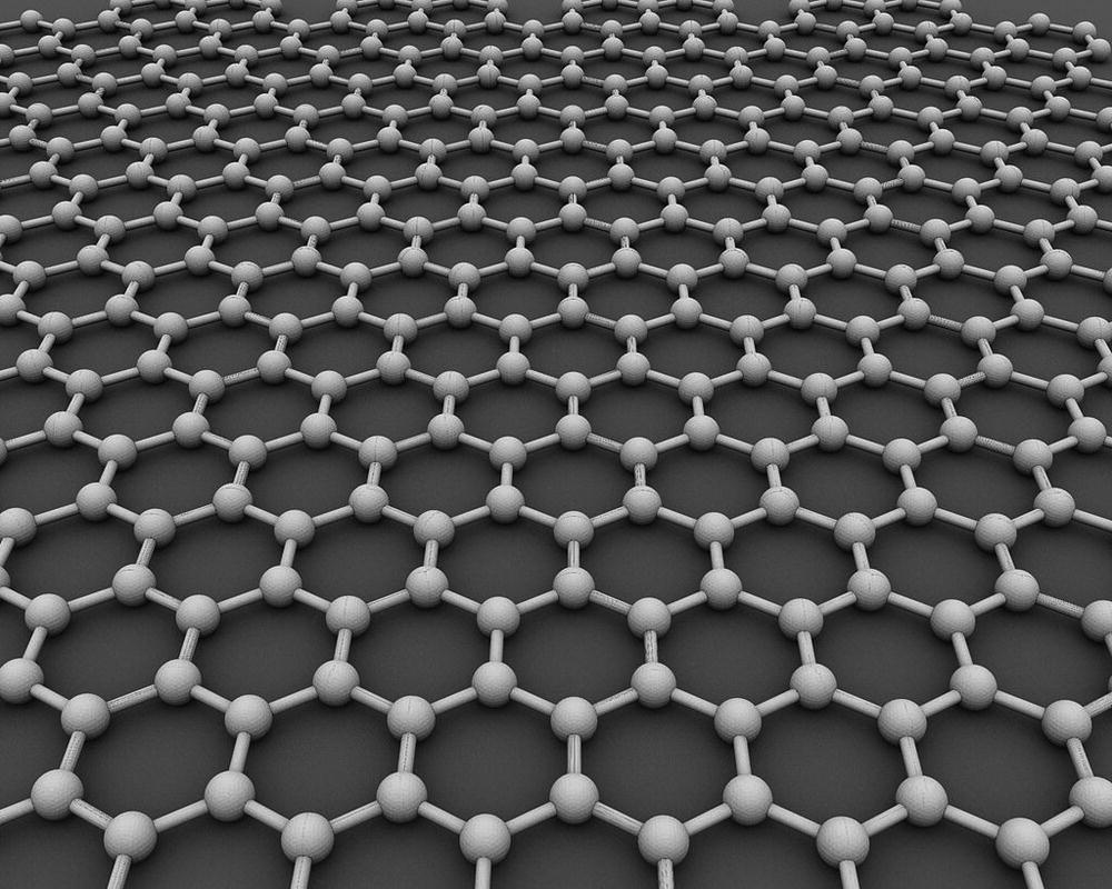
Figure 1.3 A molecular model of graphene. The almost perfect web is only one atom thick.
Source: Reprinted with permission from Ref. [50].
The honeycomb structure of graphene is formed by an infinite number of benzene rings where each carbon atom uses three of its four valence electrons to form sp2‐hybridized covalent bonds with three coplanar neighboring carbons. The fourth valence electron occupies the carbon’s pz orbital that forms sp2‐bonds shared equally in three directions, leading to a bond order of 1 and 1/3. Delocalized sp2‐electrons now spread over on a continuous layer of honeycomb constructed by short and rigid covalent bonds, and together they provide graphene an extraordinary stability to withstand a great deal of mechanical strain and stress, as indicated by its unusually high Young’s modulus value [44, 45]. On a smooth flat surface like this, any injected charge carriers can run freely at an incredibly high speed, while at the same time the graphene sheet experiences rapid lattice vibrations (i.e. phonons). Both effects contribute to the excellent electrical and thermal conductivity of this nanomaterial. Furthermore, because all carbon atoms are identical and symmetrically arranged on the honeycomb plane, graphene is nonpolar and hydrophobic except the edges. Therefore, the nanomaterial has a very poor solubility in water or even regular polar solvents used in the laboratories, which actually imposes challenges in processing graphene functionalization [46].
As a two‐dimensional crystalline membrane, graphene possesses a set of unique physical properties, collectively, surpassing any other materials known today. These properties include an exceedingly large specific surface area (2630 m2 g−1), low density (<1 g cm−3), ultrahigh charge mobility (>2 × 105 cm2 V−1 s−1), excellent electrical conductivity (106 S cm−1) and thermal conductivity (>5000 W m−1 K−1), an uniform broadband optical absorption (ultraviolet to far infrared), superb mechanical strength, and unusual flexibility [47]. So far, researchers have steered graphenes into an array of areas including some of the most popular subjects such as energy conversion and storage in fuel cells (e.g. supercapacitors), ultrafast field‐effect transistors, transparent conductors, carbocatalysis (i.e. green chemistry), chemical sensors, polymer composites, … and the list goes on. It is expected that with more research done, we will get to learn more about the full potential of graphenes and what the nanomaterials can do for the human society.
Graphenes are in the early stages of macroscale manufacturing for commercial use. They can be applied as conductive reinforcement coatings on Kevlar fibers and in the fabrication of large‐area transparent electrodes and low‐loss high‐permittivity composites, only to name a few [48]. Used in energy storage devices, graphenes support energy capacity that is cost‐effective far beyond other materials (in terms of energy per weight and cost). With all these remarkable electronic properties, graphenes are the top candidate to replace silicon‐based electronics, which is approaching its own material limit. When realized, the carbon‐based electronics promises to perform at a lightning speed with superb capacity and, now more pressingly than ever, truly green, both socially and economically.
Finally, as an endnote, Andre Geim and Konstantin Novoselov received the Nobel Prize in Physics 2010 “for groundbreaking experiments regarding the two‐dimensional material graphene” [49].
References
- 1 United States National Nanotechnology Initiative (2016). NNI supplement to the President’s 2017 Budget. https://www.nano.gov/node/1573 (accessed 16 April 2018).
- 2 National Science Foundation (2016). FY 2017 Budget Request. https://www.nsf.gov/about/budget/fy2017 (accessed 16 April 2018).
- 3 McWilliams, A. (2014). Nanotechnology: a realistic market assessment. https://www.bccresearch.com/market‐research/nanotechnology/nanotechnology‐market‐assessment‐report‐nan031f.html (accessed 16 April 2018).
- 4 Taniguchi, N. (1974). On the basic concept of nanotechnology. Proceedings of the International Conference on Production Engineering, Tokyo, Part II (Japan Society of Precision Engineering).
- 5 Feynman, R.P. (1959). There’s plenty of room at the bottom. http://calteches.library.caltech.edu/1976/1/1960Bottom.pdf. (accessed 16 April 2018).
- 6 Ito, T. and Okazaki, S. (2000). Pushing the limits of lithography. Nature 406: 1027–1031.
- 7 Binnig, G., Rohrer, H., Gerber, C., and Weibel, E. (1982). Surface studies by scanning tunneling microscopy. Phys Rev Lett 49: 57–61.
- 8 Binnig, G. and Quate, C.F. (1986). Atomic force microscope. Phys Rev Lett 56: 930–933.
- 9 The Nobel Prize in Physics 1986. Nobelprize.org. Nobel Media AB 2014. https://www.nobelprize.org/nobel_prizes/physics/laureates/1986 (accessed 16 April 2018).
- 10 Kroto, H.W., Heath, J.R., O’Brien, S.C. et al. (1985). C60: Buckminsterfullerene. Nature 318: 162–163.
- 11 United States National Nanotechnology Initiative (2018). Nanotechnology timeline. http://www.nano.gov/timeline (acessed 16 April 2018).
- 12 National Science and Technology Council Committee on Technology (2014). National Nanotechnology Initiative Strategic Plan. https://www.nano.gov/sites/default/files/pub_resource/2014_nni_strategic_plan.pdf (acessed 16 April 2018).
- 13 The National Science and Technology Council (2008). Strategy for Nanotechnology‐Related Environmental, Health and Safety Research. https://www.nano.gov/node/254 (acessed 16 April 2018).
- 14 United States National Nanotechnology Initiative (2015). Nanotechnology‐inspired grand challenges. http://www.nano.gov/grandchallenges (acessed 16 April 2018).
- 15 European Commission (2004). Towards a European strategy for nanotechnology. https://ec.europa.eu/research/industrial_technologies/pdf/policy/nano_com_en_new.pdf (acessed 16 April 2018).
- 16 European Commission (2005). Nanosciences and nanotechnologies: an action plan for Europe 2005–2009. https://ec.europa.eu/research/industrial_technologies/pdf/policy/action_plan_brochure_en.pdf (acessed 16 April 2018).
- 17 The Royal Academy of Engineering (2003). Nanoscience and nanotechnologies: opportunities and uncertainties. http://www.nanotec.org.uk/finalReport.htm (acessed 16 April 2018).
- 18 The Nobel Prize in Chemistry 2016. Nobelprize.org. Nobel Media AB 2014. https://www.nobelprize.org/nobel_prizes/chemistry/laureates/2016 (acessed 16 April 2018).
- 19 Shirai, Y., Osgood, A.J., Zhao, Y. et al. (2005). Directional control in thermally driven single‐molecule nanocars. Nano Lett 5: 2330–2334.
- 20 Greenwood, N.N. and Earnshaw, A. (1997). Chemistry of the Elements. 2e. Butterworth‐Heinemann.
- 21 Croswell, K. (1995). Alchemy of the Heavens. Anchor Book.
- 22 Roston, E. (2009). The Carbon Age. Walker & Co.
- 23 Feaver, A. (2010). The carbon age: dark element, brighter future. https://www.cnet.com/news/the‐carbon‐age‐dark‐element‐brighter‐future (acessed 16 April 2018).
- 24 American Chemical Society (2010). Discovery of fullerenes. National historic chemical landmark. https://www.acs.org/content/acs/en/education/whatischemistry/landmarks/fullerenes.html (acessed 16 April 2018).
- 25 Kroto, H.W. and Walton, D.R.M. (eds.) (1993). The Fullerenes: New Horizons for the Chemistry, Physics and Astrophysics of Carbon. Cambridge University Press.
- 26 Thompson, D.W. (1969). On Growth and Form. Cambridge University Press.
- 27 Godly, E.W. and Taylor, R. (1997). Nomenclature and terminology of fullerenes: A preliminary study. Pure Appl Chem 69: 1411–1434.
- 28 Hebard, A.F., Rosseinsky, M.J., Haddon, R.C. et al. (1991). Superconductivity at 18 K in potassium‐doped C60. Nature 350: 600–601.
- 29 Haddon, R.C. (1993). Chemistry of the fullerenes: the manifestation of strain in a class of continuous aromatic molecules. Science 261: 1545–1550.
- 30 The Nobel Prize in Chemistry 1996. Nobelprize.org. Nobel Media AB 2014. http://www.nobelprize.org/nobel_prizes/chemistry/laureates/1996 (accessed 16 April 2018).
- 31 AZoNano (2004). Carbon nanotubes – history and development of carbon nanotubes (Buckytubes). http://www.azonano.com/article.aspx?ArticleID=982 (accessed 16 April 2018).
- 32 Iijima, S. (1991). Helical microtubes of graphitic carbon. Nature 354: 56–58.
- 33 Iijima, S. and Ichihashi, T. (1993). Single shell nanotubes of 1‐nm diameter. Nature 363: 603–605.
- 34 Bethune, D.S., Kiang, C.H., Devries, M.S. et al. (1993). Cobalt‐catalyzed growth of carbon nanotubes with single‐atomic‐layer walls. Nature 363: 605–607.
- 35 Wilder, J.W.G., Venema, L.C., Rinzler, A.G. et al. (1998). Electronic structure of atomically resolved carbon nanotubes. Nature 391: 59–62.
- 36 Saito, R., Fujita, M., Dresselhaus, G., and Dresselhaus, M.S. (1992). Electronic structure of chiral graphene tubules. Appl Phys Lett 60: 2204–2206.
- 37 Hamada, N., Sawada, S.I., and Oshiyama, A. (1992). New one‐dimensional conductors: graphite microtubules. Phys Rev Lett 68: 1579–1581.
- 38 Carlson, L.J. and Krauss, T.D. (2008). Photophysics of individual single‐walled carbon nanotubes. Acc Chem Res 41: 235–243.
- 39 Avouris, P. (2002). Molecular electronics with carbon nanotubes. Acc Chem Res 35: 1026–1034.
- 40 Collins, P.G. and Avouris, P. (2000). Nanotubes for electronics. Sci Am 283: 62–69.
- 41 Kondratyuk, P. and Yates, J.T. Jr. (2007). Molecular views of physical adsorption inside and outside of single‐wall carbon nanotubes. Acc Chem Res 40: 995–1004.
- 42 Novoselov, K.S., Geim, A.K., Morozov, S.V. et al. (2004). Electric field effect in atomically thin carbon films. Science 306: 666–669.
- 43 Novoselov, K.S., Jiang, D., Schedin, F. et al. (2005). Two‐dimensional atomic crystals. Proc Natl Acad Sci USA 102: 10451–10453.
- 44 Savage, N. (2012). Materials science: super carbon. Nature 483: S30–S31.
- 45 Lee, C., Wei, X.W., Kysar, J.W., and Hone, J. (2008). Measurement of the elastic properties and intrinsic strength of monolayer graphene. Science 321: 385–388.
- 46 Quintana, M., Vazquez, E., and Prato, M. (2013). Organic functionalization of graphene in dispersions. Acc Chem Res 46: 138–148.
- 47 Allen, M.J., Tung, V.C., and Kaner, R.B. (2012). Honeycomb carbon: a review of graphene. Chem Rev 110: 132–145.
- 48 James, D.K. and Tour, J.M. (2013). Graphene: powder, flakes, ribbons, and sheets. Acc Chem Res 46: 2307–2318.
- 49 The Nobel Prize in Physics 2010. Nobelprize.org. Nobel Media AB 2014. https://www.nobelprize.org/nobel_prizes/physics/laureates/2010 (accessed 16 April 2018).
- 50 AlexanderAlUS (2010). Own Work, CC BY‐SA 3.0. https://commons.wikimedia.org/w/index.php?curid=11294534 (accessed 16 April 2018).