11
Nanoscale Quantum Sensing
Richard Feynman predicted in his 1959 speech, There’s Plenty of Room at the Bottom (Section 1.1), “When we get to the very, very small world – say circuits of seven atoms – we have a lot of new things that would happen that represent completely new opportunities for design. Atoms on a small scale behave like nothing on a large scale, for they satisfy the laws of quantum mechanics. … We can use, not just circuits, but some system involving the quantized energy levels, or the interactions of quantized spins, etc.” [1]. Indeed, 60 years later, Feynman’s “quantized spins” is today’s quantum reality.
As the name suggests, a nanoscale sensor (or nanosensor) is a device that can detect events or changes in its surrounding environment at the nanoscale or within a distance range of 1–1000 nm. The events or changes detected may be physical, chemical, or biological in nature. Examples of the use of nanosensors in the life sciences include high‐sensitivity detection of DNA and measurement of local temperature changes in living cells. In order to serve as an effective nanosensor, the device must be smaller than 100 nm and the output signals should be detectable with high sensitivity, preferably, at the single molecule or particle level. Once properly conjugated with biologically important molecules or other functional nanomaterials, these devices can be designed for use in nanomedicine such as to identify and destroy cancer cells as well as repair abnormal or damaged structures in the human body. Diamondoids and nanodiamonds, in fact, have been proposed as the building blocks of nanorobots and nanomachines for medicinal purposes [2], although realization of the concept is still far in the future.
In the previous chapters, we have demonstrated that fluorescent nanodiamonds (FNDs) containing NV− centers fulfill most of the requirements of being an ideal nanoparticle platform for biomedical applications. The sensing capability of the NV− centers, however, has not yet been explored. In this chapter, we discuss the principle and practice of using the color centers for high‐sensitivity temperature probing, along with magnetic field sensing and spin detection at the nanoscale. More applications of NV− for nanoscale quantum sensing using bulk diamonds can be found elsewhere [3] and, therefore, are not discussed here. As all these measurements are made possible by utilizing the magneto‐optical properties of the NV− centers, this chapter starts with a brief review of the spin Hamiltonian associated with this unique atom‐like quantum system.
11.1 The Spin Hamiltonian
Spin is an intrinsic property of elementary particles like the electron. It does not have a counterpart in classical mechanics and, according to quantum mechanics, is present in the form of angular momentum. The spin can interact with the orbital angular momentum to yield a total angular momentum for a given particle. Analogous to the orbital angular momentum operator, the spin angular momentum operator is a vector operator, S = (Sx, Sy, Sz), and
where Sx, Sy, and Sz are the components along the x, y, and z coordinates. The eigenvalues of S2 are
and the eigenvalues of Sz are
where S is the spin quantum number, ℏ = h/2π, and h is the Planck constant [4].
In Section 3.4, we have briefly discussed how spin–spin interactions may give rise to the crystal field splitting and how applying an external magnetic field can lift the degeneracy of the ms = ±1 sublevels of the NV− center in diamond. To describe these two types of interactions quantitatively, we write the spin Hamiltonian as [5]
where D is the spin–spin coupling tensor, ge~2.003, μB = 14.00 MHz mT–1 is the Bohr magneton, and B is the applied magnetic field. For a quantum system with axial symmetry and without crystal strains (such as NV− in a perfect diamond crystal), the Hamiltonian is given by
In the absence of the magnetic field, e.g. B = 0, the eigenvalues of the Hamiltonian of the S = 1 system are
where D is the crystal field splitting or zero field splitting. In the cases where the magnetic field is nonzero, static, and aligned along the z‐direction, the eigenvalues of the spin Hamiltonian are
The quantum mechanical description above indicates that the transitions between the electron spin states can be induced by applying microwave radiation in resonance with the crystal field splittings. When the microwave radiation is switched off, the electrons in the upper states will relax back to their lower energy states with two different decay time constants. The longer of the two time constants, T1, is often called the spin–lattice relaxation time (or longitudinal relaxation time). The shorter time constant, T2, is the spin–spin relaxation time (or transverse relaxation time). The T1 relaxation arises from equilibration of the excess spin energy with its surroundings (the lattice) through the coupling with lattice motions that have approximately the right frequency to interact with the spins. The sharing of the excess energy between spins is the cause of the T2 relaxation [5].
Another noted feature in the spin resonance spectroscopy is that, compared with stimulated emission, the spontaneous emission process in the microwave region is negligible at room temperature. According to the Einstein relation between the stimulated emission rate, Bρ(ν), and the spontaneous emission rate, A [6]:

one has
where ρ(ν) is the blackbody radiation field, c is the speed of light, h is the Planck constant, ν is the emission frequency, kB is the Boltzmann constant, and T is the temperature. At T = 300 K and ν ~ 1015 Hz as in the visible region, hν/kBT ~ 102 and thus A >> Bρ(ν). However, the relation between these two rates is reversed in the microwave region, where ν ~ 1010 Hz and A/Bρ(ν) ~ 10−3, meaning that the stimulated emission dominates over the spontaneous emission, which may be disregarded.
This brief quantum mechanics refresher of electron spins paves the way for the following discussion of nanoscale temperature sensing.
11.2 Temperature Sensing
11.2.1 Ultrahigh Precision Temperature Measurement
The NV− center in diamond is an artificial solid‐state atom with optically addressable spin states. It has a crystal field splitting of D = 2.87 GHz between ms = 0 and ±1, which can be optically read out under ambient conditions even at the single spin level with the optically detected magnetic resonance (ODMR) technique [7], as described in Section 3.4. Remarkably, the spin states have an exceptionally long coherence time (e.g. T2), capable of remaining coherent for more than 1 ms in isotope‐free bulk diamond at room temperature [8]. Both the spin resonance and coherence time of the NV− center are sensitive to the variations of temperature, magnetic field, electric field, and mechanical stress present in its environment [3]. This renders NV− a useful tool for ultra‐sensitive measurements of these physical parameters at the nanoscale, provided that the centers are implanted in nanoscale diamonds or near the surface of bulk diamonds.
Acosta et al. [9] were the first to investigate the effects of temperature on the spin resonance of the NV− centers. Using ODMR, they measured the temperature‐dependent shift of the zero field splitting from 280 to 330 K for an ensemble (10 ppb–15 ppm) of NV− in bulk diamond. A thermal shift of ΔD/ΔT = −75 kHz K−1 was determined at around 300 K and the red‐shift was attributed to thermal expansion of the diamond crystal lattice [9, 10]. Later studies over a wider temperature range for a single NV− center found that the frequency shifting is actually nonlinear with respect to temperature; for example, it may change to ΔD/ΔT = −150 kHz K−1 at 600 K [11]. A polynomial that can properly describe the temperature dependence of the spin resonance frequency over 300–700 K is [11]
where D(T) is in unit of gigahertz and T in Kelvin. While the magnitude of the thermal shift is not substantial at room temperature, it can be measured with high precision due to the exceptional stability of the ODMR spectra. Another distinctive feature of the ODMR spectra is that the widths of the spin resonance peaks show little or almost no dependence on temperature up to 600 K due to the long spin coherence time. It has an important implication for the application of single NV− centers as nanoscale thermometers over a broad temperature range, as discussed in the next section.
The concept of using FND for nanothermometry was initially disclosed in a study of thermal effects on the fluorescence lifetimes of NV− centers. With 30‐nm FNDs heated in an oven, Plakhotnik and Gruber [12] observed a 2.7‐fold decrease in the fluorescence lifetime from 300 to 670 K. The heating–cooling cycle was reversible, suggesting the potential use of this nanomaterial as a luminescence thermometer with nanometric spatial resolution. Further studies of the thermal shifts of D for FNDs showed results in good agreement with that of bulk diamond [13]. Compared with other known luminescence thermometers composed of nanoparticles such as semiconductor quantum dots, rare earth doped oxides, and gold nanoparticles (GNPs) [14, 15], FNDs stand out for having a wider range of working temperature and single‐particle detection sensitivity.
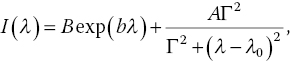
Kucsko et al. [16] reported the first application of FNDs as nanoscale thermometers in 2013. They obtained the ODMR spectra of single 100‐nm FNDs spin‐coated on a glass slide using a green laser for excitation (Figure 11.1a and b) and were able to determine the temperatures with a precision of 0.1 K or better within a measurement time of four seconds (Figure 11.1c). To induce local temperature changes, GNPs were introduced into the samples and subsequently irradiated by a separate laser to serve as the heat source (denoted in Figure 11.1b). A spatial resolution of 200 nm was achieved by measuring the separations of the nanoparticles in fluorescence images (Figure 11.1d). The results, along with other similar studies [17], showed that it is possible to detect the temperature variations at the nanoscale with a sensitivity of 0.1 K Hz−1/2 if the FNDs contain up to 1000 NV– centers per particle. Further improvement of the temperature sensing sensitivity to the 1 mK Hz−1/2 regime is achievable by utilizing the quantum coherence of single NV– spins in bulk diamonds (Figure 11.2) [16–18]. These characteristics place FND in a category of the most sensitive and stable temperature probes known to date.
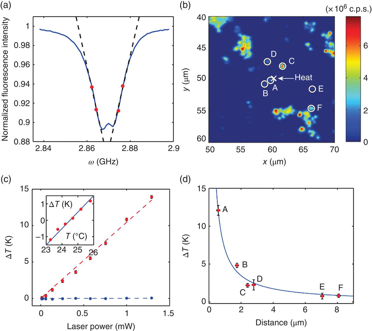
Figure 11.1 Magneto‐optical nanothermometry. (a) Frequency scan of a single FND containing approximately 500 NV− centers. The four red points indicate the measurement frequencies used to extract the temperature. (b) Two‐dimensional confocal scan of FNDs (circles) and gold nanoparticles (cross) spin‐coated onto a glass coverslip. (c) Temperature rise of a single FND as a function of laser power for two different laser‐focus locations with (red) or without (blue) laser illumination on a nearby gold nanoparticle. (d) Temperature changes measured at six FND locations, indicated by circles in (b), as a function of the distance from the illuminated gold nanoparticle indicated by the cross. The blue curve represents the best‐fitting of the temperature profile to a steady‐state solution of the heat conduction equation.
Source: Adapted with permission from Ref. [16]. Reproduced with permission of Nature Publishing Group.
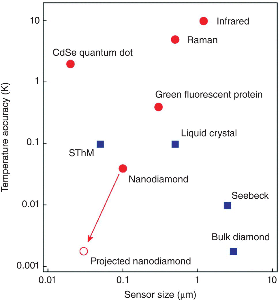
Figure 11.2 Comparison of sensor sizes and temperature accuracies for the NV‐based quantum thermometer and other reported techniques. Biocompatible methods are labeled in red. The open red circle indicates the ultimate expected accuracy for FNDs. SthM, scanning thermal microscopy.
Source: Reprinted with permission from Ref. [16]. Reproduced with permission of Nature Publishing Group.
In light of its excellent biocompatibility, a natural (and logical) application of the FND nanosensor is to measure local temperatures in living cells. Kucsko et al. [16] demonstrated this applicability by introducing FNDs and GNPs (both ~100 nm in diameter) into human embryonic fibroblast cells through nanowire‐assisted delivery. They then monitored the temperature changes of a FND particle, while locally heating a nearby GNP by a separate laser. At the laser power of 12 μW, a temperature increase of 0.5 K was measured at the FND location, corresponding to a change of approximately 10 K at the GNP location, and the cell was still alive. However, cell death occurred when the laser power was increased to 120 μW, which resulted in a temperature change of 3.9 K for the FND and 80 K at the GNP position. The results demonstrated that the technique could actively control cell viability at the nanoscale, enabling the optimization of nanoparticle‐based photothermal therapy at the single‐cell or subcellular level (cf., Section 12.2 for further discussion).
11.2.2 Time‐Resolved Nanothermometry
The plot in Figure 11.2 compares sensor sizes and temperature accuracies between the NV‐based quantum thermometer and other techniques reported in the literature [16]. The comparison clearly shows that FND outperforms other nanothermometers (such as quantum dots and green fluorescent proteins) in terms of its precision in the temperature measurement. However, a nanothermometer is far from ideal if it cannot provide information on the dynamics of underlying heat transfer phenomena. The commonly used luminescence nanothermometers, such as the lanthanide complexes [19], typically have a response time in the range of seconds. This temporal resolution by no means is sufficient to follow the time evolution of any systems under investigation at the nanoscale. Similarly for FNDs, it is a time‐consuming process (in minutes) to acquire the whole ODMR spectrum of the NV− centers. Moreover, additional data processing after the measurements is required to determine the peak positions and thus the temperature changes.
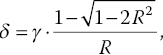
To speed up the process, Tzeng et al. [20] have developed a three‐point sampling method to determine the temperature of a system, which may or may not be necessarily in equilibrium with its surroundings, with a temporal resolution better than 10 μs. The method is based on the experimental finding that the widths of the ODMR peaks of the NV− centers are nearly invariant with temperature changes. For 100‐nm FNDs, the full width at half maximum (FWHM) of the ODMR peaks is typically 20 MHz in observation. Over the temperature range of 300–700 K, the width changes less than 10%, while the peak positions are shifted by more than 20 MHz [11]. By assuming a Lorentzian profile of constant width (γ) and measuring the intensity changes of the fluorescence dip at three preselected frequencies (Figure 11.3), the researchers have been able to determine the temperature shift (δ) without scanning the whole ODMR spectrum according to the following equations [20]:
where
and I1, I2, and I3 are the fluorescence intensities measured at points f1, f2, and f3, respectively. The method enables real‐time measurement of the temperature changes over ±100 K and, more importantly, the studies of nanoscale heat transfer dynamics in a pump‐probe configuration with a pulsed heating source.
Figure 11.3 Pictorial presentation of the three‐point method based on an ODMR spectrum consisting of only one peak. The peaks before (blue) and after (red) temperature change are both Lorentzian and have the same width, although their heights may vary. Overlaid on the spectra are three frequencies (f1, f2, f3) chosen for the intensity measurement.
Source: Reprinted with permission from Ref. [20]. Reproduced with permission of American Chemical Society.
Exploiting this unique spin resonance feature, Chang and coworkers [20] conducted time‐resolved temperature measurement for a gold nanorod solution heated by a tightly focused 808 nm laser using 100‐nm FNDs as the single‐particle temperature sensors (Figure 11.4a). With the FNDs submerged in the medium and positioned near the 808 nm laser focus, they first observed superheating of the aqueous solution near the water–glass interface from the measured ODMR spectra (Figure 11.4b) and demonstrated a measurement precision of better than ±1 K over a temperature variation range of 100 K with a spatial resolution of approximately 0.5 μm. Later, by pulsing the heating laser (808 nm), the probing laser (532 nm), as well as the microwave radiation (Figure 11.4c), a temporal resolution of 10 μs was achieved through a pump‐probe type measurement using the three‐point method (Figure 11.4d). The validity of the measurements was finally verified with finite‐element numerical simulations in this proof‐of‐principle experiment. Compared with the time‐resolved temperature measurement with dye molecules in water [21], the results represent a significant improvement of both spatial and temporal resolution by 1 and 3 orders of magnitude, respectively.
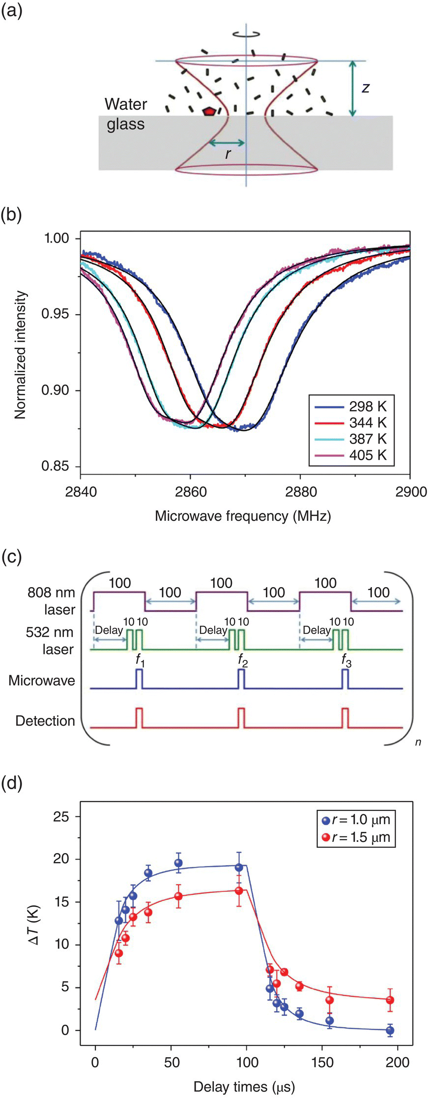
Figure 11.4 Time‐resolved nanothermometry. (a) Experimental scheme for the time‐resolved temperature measurement with a 100‐nm FND particle submerged in aqueous solution containing 10‐nm × 41‐nm GNRs (black rods) heated by an 808 nm laser (red hyperboloid). (b) ODMR spectra of the GNR solution heated by the near‐infrared laser with its power varying from 0 to 10 mW. (c) Time sequences of the laser, microwave, and detection pulses (all in μs) used in the time‐resolved nanothermometry with a three‐point method. (d) Time evolution of the heat dissipation of the GNR solution at the radial positions of r = 1.0 and 1.5 μm, as indicated in (a).
Source: Adapted with permission from Ref. [20]. Reproduced with permission of American Chemical Society.
11.2.3 All‐Optical Luminescence Nanothermometry
The thermal shifts of the spin resonances of NV− centers, as illustrated above, provide an effective means for nanoscale temperature sensing with both high temporal and spatial resolutions. However, the method is technically demanding because microwave excitation is required to deplete the fluorescence emission. Additionally, the microwave has to be delivered through a metal wire or nanostructure placed close to the systems under investigation (typically within 10 μm). The requirement of such close proximity severely limits the practical use of the OMDR technique in the life science research. Alternatively, one may focus on the thermal shift of the zero‐phonon line (ZPL) of the NV− centers. Chen et al. [10] have reported that the trend of the thermal shifting of the ZPL at 638 nm matches closely with that of the spin transitions at 2.87 GHz. At room temperature, the magnitude of the thermal shift is ΔZPL/ΔT = +0.015 nm K−1 with a FWHM approximately 5 nm for the ZPL [10, 22]. Small as it may seem, the shift is sufficient for practical temperature measurement because both the position and width of the ZPL in the fluorescence spectra are highly stable. In comparison to the temperature sensing by ODMR, this all‐optical method has the advantages of being simple, straightforward, and readily implementable by any confocal microscope equipped with a CCD‐based monochromator.
Tsai et al. [23] tried out the above idea with 100‐nm FNDs containing about 900 NV− centers per particle. Specifically, they used a 594 nm laser as the light source to avoid exciting the NV0 centers whose fluorescence emission band is partially overlapped with that of NV− at 638 nm and thus can complicate the spectral analysis. Using FNDs dispersed in water as an example, while the overall feature of the emission band does not change much with temperature over 28–75 °C, its ZPL is significantly broadened and shifted to the red as the solution temperature increases (Figure 11.5a). To determine the sensitivity of this all‐optical method, the research team spin‐coated 100‐nm FNDs on a glass coverslip and obtained their fluorescence spectra at 25 °C for the individual particles (Figure 11.5b). The ZPL centers (λ0) were then determined by fitting the spectra over 610–660 nm to a Lorentzian function along with an exponential function for the baseline correction as [24]
where I(λ) is the fluorescence intensity, λ is the wavelength, Γ is the Lorentzian half‐width, λ0 is the ZPL center, and B, b, and A are constants. Signal averaging over 6 seconds by curve‐fitting of 60 independent spectra yielded λ0 = 638.519 ± 0.013 nm at a 95% confidence interval (inset in Figure 11.5b), suggesting a temperature measurement sensitivity of ±2 K Hz−1/2. Although the effective working range of this method is limited to be less than 100 °C due to the significant band broadening as temperature increases, it is well suitable for biological applications (cf., Section 12.2).

Figure 11.5 All‐optical nanothermometry. (a) Area‐normalized temperature‐dependent fluorescence spectra of 100‐nm FNDs illuminated by a 594 nm laser in solution. Inset: Enlarged view of the temperature‐induced shift of the ZPLs for spectra acquired at 28–75 °C. (b) Typical fluorescence spectrum of a single 100‐nm FND spin‐coated on a glass coverslip at room temperature over 610–660 nm. The exposure time of the sample to the 594 nm laser with a power of 30 μW is 0.1 second. Inset: Changes of λ0 with time over six seconds, with a mean value of 638.519 ± 0.013 nm for a 95% confidence interval.
Source: Reprinted with permission from Ref. [23]. John Wiley & Sons.
In a separate study, Plakhotnik et al. [24] demonstrated an all‐optical ratiometric temperature sensor consisting of a 50‐nm FND hosting more than 100 NV− centers in the crystal matrix. Instead of detecting the thermal shift, they characterized the amplitude of the ZPL by fitting the fluorescence spectra with Eq. (11.15) and achieved a temperature measurement sensitivity of 0.3 K Hz−1/2 using a 590 nm laser for the excitation. In addition to that, a long‐term stability was attained within 0.6 K (peak‐to‐peak value) for a single 50‐nm FND spin‐coated on a glass substrate and imaged with a home‐built microscope system. Although the method is intrinsically more sensitive than the detection of the ZPL shift, it is more susceptible to the interference from background (or baseline) signals. Fortunately, the background interference can be properly removed by conducting either fluorescence lifetime gating or magnetic modulation as discussed in Section 6.2.
11.2.4 Scanning Thermal Imaging
Thermal mapping is a process by which the spatial variation of the temperature of an object is measured. While feasible, it remains a challenge to apply the single‐particle FND nanothermometry for any practical thermal mapping at the nanoscale. In particular, to conduct the mapping, the FND probe must be scanned through the sample in order to obtain information about the spatial temperature distribution. To meet the challenge, Tetienne et al. [25] grafted a single FND particle (~100 nm in diameter) as a thermal probe onto the tip of an atomic force microscope (AFM). Hosting an ensemble of spins (~100 NV− centers), the FND provided a significantly improved acquisition time by as much as an order of magnitude. Additionally, the combination of these two techniques preserved the sub‐100‐nm spatial resolution inherited from the scanning probe microscope for both temperature sensing and topographic imaging. The researchers applied this method, in conjunction with ODMR, to map the local temperature rise due to laser irradiation of a single 40‐nm GNP submerged in aqueous solution (cf., captions in Figure 11.6 for details). The results pave the way toward new applications of the FND nanothermometry in areas such as thermal imaging of material processing and microelectronic devices in operation.
Figure 11.6 Thermal imaging of a laser‐heated gold nanoparticle. (a) Schematic diagram of the experimental design. Both the AFM tip and the gold nanoparticle are immersed in water to ensure thermal equilibrium between the probe and the sample. (b, c) Fluorescence image (b) and temperature map (c) obtained simultaneously by scanning a 40‐nm gold nanoparticle relative to the FND probe and its excitation laser. (d) ODMR spectra corresponding to three different pixels of the scan, located as indicated by the crosses in (b) with matching colors. (e) Line cuts extracted from (b) and (c) taken along the dashed lines shown in (b) with matching colors. The black solid curve is a fit of the experimental data to a theoretical model.
Source: Adapted with permission from Ref. [25]. Reproduced with permission of American Chemical Society.
Besides mapping nanoscale temperature changes, the FND nanothermometry is also capable of imaging the thermal conductivity (k) of a nanostructure. With this perspective, Laraoui et al. [26] attached a FND to the apex of a silicon tip of an AFM as a local temperature sensor. They then applied an electrical current to heat up the tip and brought the FND in contact with a surface of varying thermal conductivities with nanometer precision. The fast response time (<200 μs) of the sensor, due to its small size and high thermal conductivity, made it possible to study the nanoscale heat transfer dynamics triggered by an electrical pulse. By combining AFM and confocal fluorescence microscopy, the researchers attained excellent matching between thermal conductivity and topographic maps for a phantom microstructure made of a gold grid (k = 314 W m−1K−1) on a sapphire substrate (k = 30 W m−1K−1) with distinct thermal conductivities between these two materials. Such an integrated method promises multiple applications, ranging from the investigation of phonon dynamics in nanostructures to the characterization of heterogeneous phase transitions and chemical reactions in various solid‐state systems.
11.3 Magnetic Sensing
11.3.1 Continuous‐Wave Detection
In 1997, Wrachtrup and coworkers [7] demonstrated for the first time that the electron spin resonance spectra of a single NV− center in a bulk diamond could be optically read out at the single‐molecule level by using the ODMR technique. In the absence of crystal strain, the spin resonance spectrum showed a single peak at 2.87 GHz, which would split into two if an external magnetic field was applied to the NV− center, as verified by experiments (Figure 3.9) [27]. Mathematically, it has been shown that at B << D/γe, the two components of the splitting have the frequencies of [28]
where γe = geμB/h= 28.03 MHz mT−1 and θB is the angle between the magnetic field and the NV− center’s major symmetry axis. Using this equation, one can accurately determine the strength of the external magnetic field based on the observed Zeeman splittings with the NV− center as a highly sensitive magnetic sensor. However, as pointed out by Schirhagl et al. [3], while the method is direct, the detection sensitivity is compromised by the significant broadening of the spin resonance bands. Much enhancement of the sensitivity can be gained by changing the detection to the pulsed modes, which take advantage of the NV− center’s long coherence time in bulk diamond as well as the many refined microwave sequences that have been developed over the past few decades for magnetic resonance spectroscopy [29]. The combination of this unique spin system and the ODMR technique has enabled ultrasensitive and rapid detection of single electronic spin states under ambient conditions for nanoscale magnetic resonance imaging [30].
Some research groups have applied FNDs as a nanoscale imaging magnetometer to detect weak magnetic fields using the continuous‐wave approach [27, 31]. Specifically, Balasubramanian et al. [27] incorporated a 40‐nm FND hosting a single NV− center into the cantilever of an AFM (Figure 11.7a and b) and applied the cantilever with the ODMR setup as a scanning probe microscope to achieve subwavelength imaging resolution of a nickel nanostructure. Additionally, by applying microwaves resonant at 2.750 GHz to the NV− center, they observed a narrow dark line close to the corner of the triangular structure (Figure 11.7c). The width of the line was about 20 nm, corresponding to a measurement resolution of 0.5 mT.

Figure 11.7 Scanning probe magnetometry. (a) Diagram of the magnetic field imaging experiment. A magnetic nanoparticle (red) is imaged with a single NV− in FND (green dot within the blue nanocrystal) fixed at the scanning probe tip (black). (b) Optical image of a FND attached to an AFM tip. The scattered light image of the tip is overlapped with the fluorescence image of the nanocrystal. The bright red spot (arrowed) represents fluorescence of the single NV−. (c) Field reconstruction using the scanning probe single spin magnetometer, showing an AFM image of a nickel magnetic nanostructure (top left), a magneto‐optical image of the same structure (bottom left), and the fluorescence signal when resonant microwaves at 2.750 GHz are applied to the NV− center.
Source: Reprinted with permission from Ref. [27]. Reproduced with permission of Nature Publishing Group.
Using a similar setup, Rondin et al. [31] conducted nanoscale magnetic imaging with a FND‐attached AFM tip to measure large off‐axis magnetic fields, which could induce spin level mixing and thus change the fluorescence intensity (Section 3.4). The method was all‐optical, requiring no microwave control, and hence expanding the operation range of the NV‐based magnetometry. The performance of the FND‐scanning probe magnetometer was demonstrated by mapping the magnetic field distribution created by a commercial magnetic hard disk. A sensitivity of 10 μT Hz−1/2 was reported by the researchers in this study. The ultimate accuracy of these magnetic field measurements is about 20 μT, limited by the couplings of the NV− centers with paramagnetic entities such as other NV centers, 13C, and 14N nuclei in the FNDs [32].
To demonstrate the chemical sensing capability of the FND‐based luminescence magnetometry, Lim et al. [33] integrated the NV‐based magnetic sensor with a microfluidic system. They manipulated a single magnetic particle in three dimensions in a microfluidic device with a combination of planar electro‐osmotic flow control and vertical magnetic actuation, and then applied a fixed FND hosting a single NV− center to measure the strength of the magnetic field generated by the magnetic particle at a separation distance of 7.25 μm (Figure 11.8a), 3.62 μm (Figure 11.8b), and 1.50 μm (Figure 11.8c). From the peak shifts in the ODMR spectra, the magnetic field distribution was mapped out with nanometer accuracy. Their result compared favorably with the calculated magnetic field intensity of a model magnetic dipole as a function of distance from the FNDs.
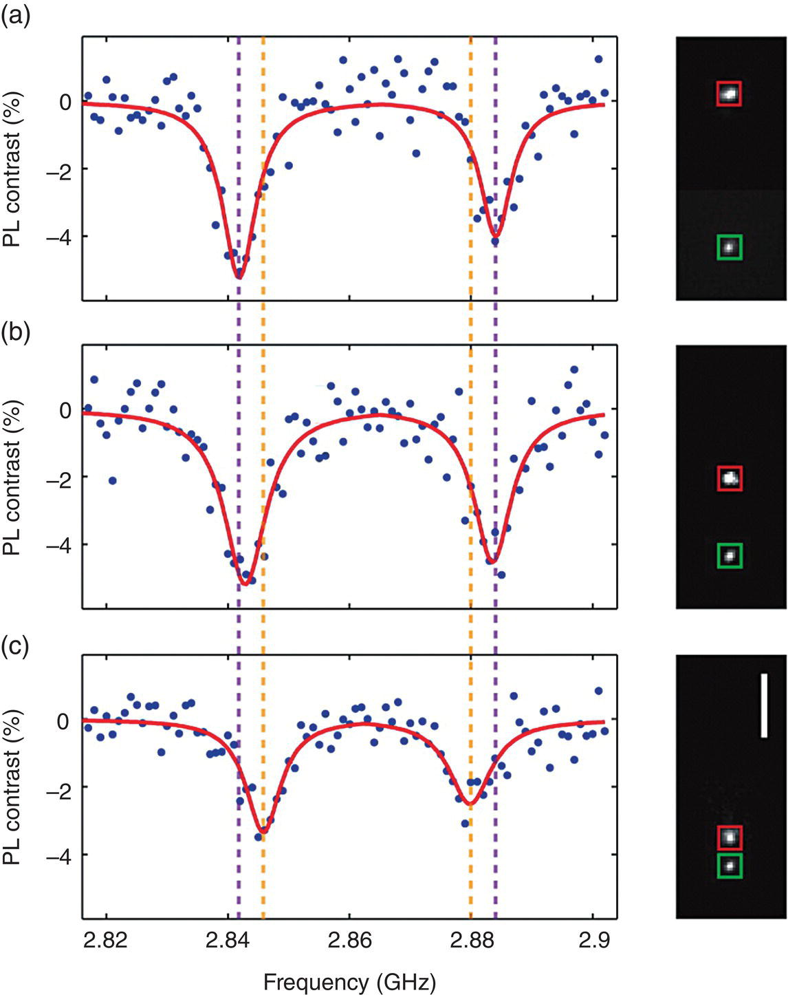
Figure 11.8 ODMR spectra (left) and camera images (right) of a magnetic nanoparticle (red square) and a FND (green square) separated by a distance of (a) 7.25 μm, (b) 3.62 μm, and (c) 1.50 μm. Red curves in the spectra are Lorentzian fits to the measured data and dashed lines in purple and orange are the center frequencies of the Lorentzian fits in (a) and (c), respectively. PL, photoluminescence. Scale bar: 3 μm.
Source: Reprinted with permission from Ref. [33]. Reproduced with permission of American Chemical Society.
Taking a different approach, Horowitz et al. [34] applied an infrared laser as an optical tweezer for the three‐dimensional control of a single 100‐nm FND particle in solution. Despite the motion and random orientation of the FND in the trap, they were able to observe distinct peaks in the ODMR spectra of an ensemble of NV− centers in the particle. Similarly, Kayci et al. [35] employed an anti‐Brownian electro‐kinetic trap to manipulate a single FND particle under ambient and aqueous conditions for magneto‐optical spin detection. Furthermore, Geiselmann et al. [36] developed a deterministic optical trapping technique and demonstrated the three‐dimensional manipulation of individual FNDs hosting multiple NV− centers to measure the local magnetic field in a glycerol–water mixture. The development of all these techniques has opened new opportunities to probe the magnetic fields in complex environments such as the interiors of microfluidic channels and live cells that are inaccessible by the scanning probe techniques existing today.
Developed originally to study condensed‐phase phenomena, the magnetic sensing techniques discussed above have also been applied to using the NV− centers as nanoprobes in the gas phase [37–39]. For example, Hoang et al. [38] optically levitated a 100‐nm FND particle for electron spin control of its built‐in NV− centers in low vacuum. Measuring the absolute internal temperature of the levitated FNDs by ODMR, the researchers observed an enhancement in the strength of the spin resonance signal as the air pressure was reduced, suggesting that oxygen gases could exert an effect on both the fluorescence intensity and the ODMR contrast. The study implies a potential application of NV− for sensing gaseous oxygen, which has two unpaired electrons and is paramagnetic.
11.3.2 Relaxometry
Now we turn to the pulsed operations. As discussed in the previous section, the pulsed operations may provide a more sensitive means for magnetic sensing. Relaxometry is one of such techniques, which are traditionally used in nuclear magnetic resonance spectroscopy to measure nuclear spin relaxation rates that depend strongly on the fluctuations of the magnetic fields in microscopic environments. The technique is adopted here to monitor the relaxation of NV− centers by optically polarizing its ms = 0 state and then measuring the probability of finding the spins recovered in the same state at a later time, T1, i.e. the spin–lattice relaxation time [40–44]. Time‐resolved measurements with a temporal resolution in the range of one minute are readily achievable with this technique [44].
With the relaxometry, Ermakova et al. [42] demonstrated the detection of a few ferritin molecules loaded on a single FND particle hosting multiple NV− centers. Ferritin is an iron storage protein capable of transporting as many as 4500 atoms of Fe with a magnetic moment of 300 μB. The researchers first attached ferritin to the surface of a 40‐nm FND by noncovalent conjugation to form ferritin–FND complexes. From a comparison of the measured T1 relaxation times between free FNDs and the ferritin–FND complexes for more than 30 particles in each group, a significant reduction of the T1 time (from 41.8 μs of free FNDs to 5.7 μs of the ferritin–FND complexes) due to the protein conjugation was found. Compared with existing magnetic force microscopy techniques, the method has an unmatched advantage in that it does not require cryogenic temperature or vacuum, a major improvement in a practical sense.
In a proof‐of‐principle experiment for biological sensing with the relaxometry, Kaufmann et al. [43] applied the single NV− centers in FNDs to detect gadolinium (Gd) spin labels in an artificial cell membrane under ambient conditions (cf., captions in Figure 11.9 for details). The Gd3+ ion is a common magnetic resonance imaging contrast agent with spin 7/2 and it can bind with the negatively charged head of the lipid molecule in a supported lipid bilayer by electrostatic forces. The Gd‐labeled lipids can thus produce considerable magnetic fluctuations in the artificial membrane by a combined effect of Gd–Gd spin dipole interactions, motional diffusion, and intrinsic Gd spin relaxation. The researchers found that the T1 relaxation times of the membrane‐bound FNDs were significantly shortened when the artificial membrane was labeled with 10% Gd spin‐labeled lipids, suggesting a sensitivity of approximately 5 Gd spins Hz−1/2. The ability to detect such a small number of spins in a model biological setting has established a new avenue for in situ nanoscale investigation of the dynamical processes in a single living cell.

Figure 11.9 Schematic of the nanoscopic detection of spin labels in an artificial cell membrane using a single‐spin FND sensor. (a) A supported lipid bilayer (SLB) formed around a FND immobilized on a glass substrate. (b) A FND hosting a single NV− center acting as a single‐spin sensor by virtue of the magnetic levels in the ground state. (c) A Gd3+ ion binding with a lipid molecule in the SLB. (d) Gd spin labels causing magnetic field fluctuations that affect the quantum states of the NV− centers in FNDs, measured through its spin–lattice relaxation time, T1. (e) Electronic energy structure of the NV− center, showing the fluorescence cycle and optical spin readout of the spin states, ms = 0 and ±1, and the protocol for the T1 measurement. (f) Schematic illustration of the T1 measurement. The relaxation of the NV spin in the target environment is compared with that in the reference environment. Measurement at a single time point in the evolution allows faster detection.
Source: Reprinted with permission from Ref. [43].
References
- 1 Feynman, R.P. (1959). There’s plenty of room at the bottom. http://calteches.library.caltech.edu/1976/1/1960Bottom.pdf (accessed 16 April 2018).
- 2 Freitas, R.A. Jr. (2003). Nanomedicine (Vol IIA): Biocompatibility. Landes Bioscience.
- 3 Schirhagl, R., Chang, K., Loretz, M., and Degen, C.L. (2014). Nitrogen‐vacancy centers in diamond: nanoscale sensors for physics and biology. Annu Rev Phys Chem 65: 83–105.
- 4 Levine, I.N. (1983). Quantum Chemistry, 3e. Allyn and Bacon.
- 5 Atherton, N.M. (1993). Principles of Electron Spin Resonance. Ellis Horwood, PTR Prentice Hall.
- 6 Atkins, P. and de Paula, J. (2006). Atkins’ Physical Chemistry. Oxford: Oxford University Press.
- 7 Gruber, A., Drabenstedt, A., Tietz, C. et al. (1997). Scanning confocal optical microscopy and magnetic resonance on single defect centers. Science 276: 2012–2014.
- 8 Balasubramanian, G., Neumann, P., Twitchen, D. et al. (2009). Ultralong spin coherence time in isotopically engineered diamond. Nat Mater 8: 383–387.
- 9 Acosta, V.M., Bauch, E., Ledbetter, M.P. et al. (2010). Temperature dependence of the nitrogen‐vacancy magnetic resonance in diamond. Phys Rev Lett 104: 070801.
- 10 Chen, X.D., Dong, C.H., Sun, F.W. et al. (2011). Temperature dependent energy level shifts of nitrogen‐vacancy centers in diamond. Appl Phys Lett 99: 161903.
- 11 Toyli, D.M., Christle, D.J., Alkauskas, A. et al. (2012). Measurement and control of single nitrogen‐vacancy center spins above 600 K. Phys Rev X 2: 031001.
- 12 Plakhotnik, T. and Gruber, D. (2010). Luminescence of nitrogen‐vacancy centers in nanodiamonds at temperatures between 300 and 700 K: perspectives on nanothermometry. Phys Chem Chem Phys 12: 9751–9756.
- 13 Plakhotnik, T., Doherty, M.W., Cole, J.H. et al. (2014). All‐optical thermometry and thermal properties of the optically detected spin resonances of the NV− center in nanodiamond. Nano Lett 14: 4989–4996.
- 14 Brites, C.D., Lima, P.P., Silva, N.J. et al. (2012). Thermometry at the nanoscale. Nanoscale 4: 4799–4829.
- 15 Jaque, D. and Vetrone, F. (2012). Luminescence nanothermometry. Nanoscale 4: 4301–4326.
- 16 Kucsko, G., Maurer, P.C., Yao, N.Y. et al. (2013). Nanometer‐scale thermometry in a living cell. Nature 500: 54–58.
- 17 Neumann, P., Jakobi, I., Dolde, F. et al. (2013). High‐precision nanoscale temperature sensing using single defects in diamond. Nano Lett 13: 2738–2742.
- 18 Toyli, D.M., de las Casas, C.F., Christle, D.J. et al. (2013). Fluorescence thermometry enhanced by the quantum coherence of single spins in diamond. Proc Natl Acad Sci USA 110: 8417–8421.
- 19 Piñol, R., Brites, C.D., Bustamante, R. et al. (2015). Joining time‐resolved thermometry and magnetic‐induced heating in a single nanoparticle unveils intriguing thermal properties. ACS Nano 9: 3134–3142.
- 20 Tzeng, Y.K., Tsai, P.C., Liu, H.Y. et al. (2015). Time‐resolved luminescence nanothermometry with nitrogen‐vacancy centers in nanodiamonds. Nano Lett 15: 3945–3952.
- 21 Cordero, M.L., Verneuil, E., Gallaire, F., and Baroud, C.N. (2009). Time‐resolved temperature rise in a thin liquid film due to laser absorption. Phys Rev E 79: 011201.
- 22 Doherty, M.W., Acosta, V.M., Jarmola, A. et al. (2014). Temperature shifts of the resonances of the NV− center in diamond. Phys Rev B 90: 041201(R).
- 23 Tsai, P.C., Epperla, C.P., Huang, J.S. et al. (2017). Measuring nanoscale thermostability of cell membranes with single gold‐diamond nanohybrids. Angew Chem Int Ed 56: 3025–3030.
- 24 Plakhotnik, T., Aman, H., and Chang, H.C. (2015). All‐optical single‐nanoparticle ratiometric thermometry with a noise floor of 0.3 K·Hz−1/2. Nanotechnology 26: 245501.
- 25 Tetienne, J.P., Lombard, A., Simpson, D.A. et al. (2016). Scanning nanospin ensemble microscope for nanoscale magnetic and thermal imaging. Nano Lett 16: 326–333.
- 26 Laraoui, A., Aycock‐Rizzo, H., Gao, Y. et al. (2015). Imaging thermal conductivity with nanoscale resolution using a scanning spin probe. Nat Commun 6: 8954.
- 27 Balasubramanian, G., Chan, I.Y., Kolesov, R. et al. (2008). Nanoscale imaging magnetometry with diamond spins under ambient conditions. Nature 455: 648–651.
- 28 Doherty, M.W., Michl, J., Dolde, F. et al. (2014). Measuring the defect structure orientation of a single NV− centre in diamond. New J Phys 16: 063067.
- 29 Slichter, C.P. (1990). Principles of Magnetic Resonance, 3e. Springer.
- 30 Rugar, D., Mamin, H.J., Sherwood, M.H. et al. (2015). Proton magnetic resonance imaging using a nitrogen‐vacancy spin sensor. Nat Nanotechnol 10: 120–124.
- 31 Rondin, L., Tetienne, J.P., Spinicelli, P. et al. (2012). Nanoscale magnetic field mapping with a single spin scanning probe magnetometer. Appl Phys Lett 100: 153118.
- 32 Aman, H. and Plakhotnik, T. (2016). Accuracy in the measurement of magnetic fields using nitrogen‐vacancy centers in nanodiamonds. J Opt Soc Am B 33: B19–B27.
- 33 Lim, K., Ropp, C., Shapiro, B. et al. (2015). Scanning localized magnetic fields in a microfluidic device with a single nitrogen vacancy center. Nano Lett 15: 1481–1486.
- 34 Horowitz, V.R., Alemán, B.J., Christle, D.J. et al. (2012). Electron spin resonance of nitrogen‐vacancy centers in optically trapped nanodiamonds. Proc Natl Acad Sci USA 109: 13493–13497.
- 35 Kayci, M., Chang, H.C., and Radenovic, A. (2014). Electron spin resonance of nitrogen‐vacancy defects embedded in single nanodiamonds in an ABEL trap. Nano Lett 14: 5335–5341.
- 36 Geiselmann, M., Juan, M.L., Renger, J. et al. (2013). Three‐dimensional optical manipulation of a single electron spin. Nat Nanotechnol 8: 175–179.
- 37 Neukirch, L.P., von Haartman, E., Rosenholm, J.M., and Vamivakas, A.N. (2015). Multi‐dimensional single‐spin nano‐optomechanics with a levitated nanodiamond. Nat Photon 9: 653–657.
- 38 Hoang, T.M., Ahn, J., Bang, J., and Li, T. (2016). Electron spin control of optically levitated nanodiamonds in vacuum. Nat Commun 7: 12250.
- 39 Kumar, P. and Bhattacharya, M. (2017). Magnetometry via spin‐mechanical coupling in levitated optomechanics. Opt Express 25: 19568–19582.
- 40 Ziem, F.C., Götz, N.S., Zappe, A. et al. (2013). Highly sensitive detection of physiological spins in a microfluidic device. Nano Lett 13: 4093–4098.
- 41 Steinert, S., Ziem, F., Hall, L.T. et al. (2013). Magnetic spin imaging under ambient conditions with sub‐cellular resolution. Nat Commun 4: 1607.
- 42 Ermakova, A., Pramanik, G., Cai, J.M. et al. (2013). Detection of a few metallo‐protein molecules using color centers in nanodiamonds. Nano Lett 13: 3305–3309.
- 43 Kaufmann, S., Simpson, D.A., Hall, L.T. et al. (2013). Detection of atomic spin labels in a lipid bilayer using a single‐spin nanodiamond probe. Proc Natl Acad Sci USA 110: 10894–10898.
- 44 Rendler, T., Neburkova, J., Zemek, O. et al. (2017). Optical imaging of localized chemical events using programmable diamond quantum nanosensors. Nat Commun 8: 14701.