
Semiconductor Spintronics: Progress and Challenges
Dept. of Physics, Harvard University, Cambridge, MA 02138, U.S.A.
1. Introduction
Spin is the only internal degree of freedom of the electron, and utilizing it in the new generations of semiconductor devices is the main goal of semiconductor spintronics. Contemporary semiconductor electronics is based on electron charge only. It is expected that spin-based phenomena will provide electronic devices with new functionality, and achieving quantum computing with electron spins is among the most ambitious goals of spintronics.1,2 During the last five years, there has been impressive progress in this field, both in experiment and in developing theoretical concepts. Since the goals are highly challenging and require overcoming a number of difficult problems, research is developing along several avenues. For example, the prospects of spin-based computing with quantum dots require an increase in the spin coherence time of gate-controlled double quantum dots by several orders of magnitude, and a great advance in this direction has been achieved recently by applying spin echo techniques.3 In what follows, we concentrate on fundamentals and on recent developments related to a different branch of spintronics: the use of spin-orbit coupling to achieve direct electrical control of electron spins in semiconductor nanostructures. Compared with magnetic control, electrical control holds promise of much higher efficiency, as well as access to electron spins on the nanoscale.
Strong enhancement of spin-orbit coupling in crystals as compared to vacuum originates from the large gradients of crystal field ![]() V(r) and high electron velocities v near nuclei. The enhanced spin-orbit coupling affects the wave-functions and energy spectra of Bloch states. In vacuum, the dimensionless parameter of spin-orbit coupling is about E(k)/m0c2 ~ 10-6, with the electron energy E(k) ~ 1 eV and the Dirac gap m0c2 ~ 1 MeV. In semiconductors, the similar parameter is ΔSO/EG ~ 1, where ΔSO ~ 1 eV is the spin-orbit splitting of valence bands and the EG ~ 1 eV is the bandgap. This enhancement makes semiconductors promising for electrical manipulation of electron spins.4
V(r) and high electron velocities v near nuclei. The enhanced spin-orbit coupling affects the wave-functions and energy spectra of Bloch states. In vacuum, the dimensionless parameter of spin-orbit coupling is about E(k)/m0c2 ~ 10-6, with the electron energy E(k) ~ 1 eV and the Dirac gap m0c2 ~ 1 MeV. In semiconductors, the similar parameter is ΔSO/EG ~ 1, where ΔSO ~ 1 eV is the spin-orbit splitting of valence bands and the EG ~ 1 eV is the bandgap. This enhancement makes semiconductors promising for electrical manipulation of electron spins.4
2. Basic concepts of semiconductor spintronics
Apparently, the first practical application of electrically-driven spin transitions belongs to laser physics and dates back as far as 1971.5 More recent research was initiated by the 1990 paper of Datta and Das, who advanced the idea of a spin-transport device based on spin interference in media with spin-orbit coupling.6 Afterwards, this device became known as a spin transistor. Despite the fact that the attempts to fabricate such a device have not been successful to date and its feasibility has been questioned,7 the basic principles underlying it strongly influenced subsequent research.
A toy-model spin-orbit Hamiltonian describing electrons in asymmetric two-dimensional (2D) systems (Rashba term8,9) is
where α is the spin-orbit coupling constant, σ is the Pauli matrix vector, k is electron wavevector, and z0 is a unit vector perpendicular to the confinement plane. When rewritten as
where μB is the Bohr magneton and Bα(k)is an effective momentum-dependent spin-orbit field, the Hamiltonian Hα describes spin precession in the field Bα(k). The same phenomenon can be also understood in terms of two eigenstates of the Hamiltonian Hα with the same propagation direction k0 and energy E, but with different momenta k± depending on the spin-orbit coupling constant α (spin birefringence). Therefore, if spin-polarized electrons are injected at x = 0 along the direction k0 in a spin state that is not an eigenstate for the field Bα(k), the resistance of the device is controlled by the α-dependent phase of the electron wave function near the spin-polarized drain at x = L.
The proposed Datta and Das device is based on the following principles:
- spin injection from a ferromagnetic source and spin detection by a ferromagnetic drain;
- electrical control of spin-orbit coupling α by a Schottky gate;
- spin precession in the spin-orbit field Bα; and
- spin interference.
Lately, there has been impressive progress in developing ferromagnetic injectors, including better understanding of the role of contacts between spin injectors and semiconductor microstructures. At the same time, much research effort has been focused on generating and injecting spin populations electrically, by means of spin-orbit coupling, as avoiding ferromagnetic elements would allow the elimination of stray magnetic fields. Electrical control of spin-orbit coupling10,11 and spin precession12 in the field Bα have been reported long ago, while spin interference has been observed only recently, as discussed in Section 4 below.
All-semiconductor electrically controlled spintronics needs a better understanding spin transport in media with spin-orbit coupling that is rather nontrivial. In what follows, we review some of the recent progress in this field.
3. The origin of spin coupling to external electric field
Electrically induced quantum transitions are usually described in terms of oscillator strengths that are subject to the oscillator sum rule (Thomas-Kuhn-Reiche theorem). This sum rule follows from the standard commutation relation
When this commutation relation is written as a sum over the intermediate states, it becomes a sum of the terms
which are oscillator strengths of n ← ![]() transitions. In the absence of spin-orbit coupling, calculating the commutator of the coordinate x and the Hamiltonian, we find
transitions. In the absence of spin-orbit coupling, calculating the commutator of the coordinate x and the Hamiltonian, we find
and after substitution into Eq. (4) we arrive at
where m0 is the electron mass in vacuum. For local states, the oscillator sum rule
includes nondiagonal n ≠ ![]() terms only, as the diagonal n =
terms only, as the diagonal n = ![]() terms vanish because matrix elements of the coordinate x in Eq. (5) are finite.
terms vanish because matrix elements of the coordinate x in Eq. (5) are finite.
However, because Bloch states are extended, diagonal matrix elements of x diverge. Hence, diagonal matrix elements of k may survive. Observing that the oscillator strengths fn←![]() of Eq. (6) coincide, with accuracy up to the factor m0, with the summands in the standard expression of k·p theory for the inverse effective mass m
of Eq. (6) coincide, with accuracy up to the factor m0, with the summands in the standard expression of k·p theory for the inverse effective mass m![]() in the
in the ![]() th Bloch band, one arrives at the equation
th Bloch band, one arrives at the equation
Therefore, m0/m![]() is the oscillator strength, f
is the oscillator strength, f![]() ←
←![]() for the transition from the state
for the transition from the state ![]() “into itself”.13 This is precisely the oscillator strength that manifests itself in the Drude and cyclotron absorption.
“into itself”.13 This is precisely the oscillator strength that manifests itself in the Drude and cyclotron absorption.
The problem we need to solve is what happens to this oscillator strength in a noncentrosymmetric system when spin-orbit coupling enters the picture, α ≠ 0, and a spin-degenerate band splits into two subbands. This situation is illustrated in Fig. 1. For each state, the total oscillator strength m0/m![]() is divided between the transition “into itself” and the transition between branches. For the transitions from the bottom of the band, the inter-branch transition energy equals 2ESO, with ESO = m
is divided between the transition “into itself” and the transition between branches. For the transitions from the bottom of the band, the inter-branch transition energy equals 2ESO, with ESO = m![]() α2/
α2/![]() 2, and the oscillator strength is divided equally between both transitions. For a given wavevector k, electron spins have opposite directions on two branches of the energy spectrum and hence inter-branch transitions are spin-flip transitions. These transitions have high oscillator strengths, comparable to the oscillator strength of the cyclotron resonance. With increasing electron energy, intensities of inter-branch transitions decrease, but only as kα/kF, where kα = m
2, and the oscillator strength is divided equally between both transitions. For a given wavevector k, electron spins have opposite directions on two branches of the energy spectrum and hence inter-branch transitions are spin-flip transitions. These transitions have high oscillator strengths, comparable to the oscillator strength of the cyclotron resonance. With increasing electron energy, intensities of inter-branch transitions decrease, but only as kα/kF, where kα = m![]() α/
α/![]() 2 is the spin precession momentum in the field Bα(k), and kF is Fermi momentum. Therefore, their intensities remain high for reasonable α values. Outside the spectral region of interbranch transitions, their Kramers-Kronig transform describes spin coupling to electric fields;14 spectral dependence of the corresponding sponse can be only found from detailed transport equations. In a strong magnetic-field B, inter-branch transitions transform into the electric dipole spin resonance (EDSR), whose intensity is usually much higher than the intensity of electron paramagnetic resonance (EPR).4,8
2 is the spin precession momentum in the field Bα(k), and kF is Fermi momentum. Therefore, their intensities remain high for reasonable α values. Outside the spectral region of interbranch transitions, their Kramers-Kronig transform describes spin coupling to electric fields;14 spectral dependence of the corresponding sponse can be only found from detailed transport equations. In a strong magnetic-field B, inter-branch transitions transform into the electric dipole spin resonance (EDSR), whose intensity is usually much higher than the intensity of electron paramagnetic resonance (EPR).4,8
The important role that intrabranch transitions play in spin transport will be discussed in Section 6 below.
4. Experimental achievements: Spin populations and spin interference
Because of the spin coupling to electric field, propagation of electric current across a sample is accompanied by spin accumulation in the bulk of three-dimensional (3D) and 2D systems.15,16 For thin 3D layers and 2D systems, this was recently observed by Kato et a1.,17 Silov et al., and Ganichev et al.19 Another related phenomenon is spin Hall effect20-22 that manifests itself in spin accumulation near the edges of a sample, for review see Refs. 23 and 24. Spin Hall effect observed in n-GaAs25 was attributed to an extrinsic mechanism, whereas the effect observed in p-GaAs26 was taken to be intrinsic – that is, the former effect originates from impurity scattering, whereas the latter is due to spin-orbit coupling in the bulk.
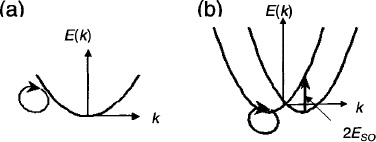
Figure 1. Spin-degenerate spectrum in the absence of spin orbit coupling (a) and spin-split spectrum of 2D electrons with spin-orbit coupling of Eq. (1) (b). In (a), the oscillator strength for transitions “into itself” (a circle with an arrow) equals mo/m![]() . In (b), this oscillator strength is divided between transitions “into itself” and transitions between two branches (vertical arrow). For the transitions from the bottom of the band (shown in the figure), the oscillator strength mo/m
. In (b), this oscillator strength is divided between transitions “into itself” and transitions between two branches (vertical arrow). For the transitions from the bottom of the band (shown in the figure), the oscillator strength mo/m![]() , is equally divided between both types of transitions.
, is equally divided between both types of transitions.
Spin interference phenomena, besides their promise for applications, are important from the fundamental point of view because they are related to quantum phases that essentially depend on the shape of the electron paths. In particular, these phases differ for rings, where electron motion is close to adiabatic, and polygons where motion near vertices is strongly nonadiabatic. Spin interference on a large array of InGaAs square loops was reported by Koga et a1.,27 and on a single HgTe/HgCdTe ring by Koenig et al.28
5. Enhancing spin responses to electric fields
Long delay in the experimental observation of electrically driven spin populations in 2D systems after their prediction was caused by the small magnitude of these effects. The weakness of the effect also hinders its utilization in semiconductor devices. In this Section, we discuss some options for enhancing spin response.
- Spin response to an inhomogeneous dc electric field F(r) = F0exp(iq·r) diverges when q → 2kα.29 This behavior can be easily understood if one takes into account that adding wavevector q results in a mutual displacement of two Fermi surfaces with the same energy, and for q = 2kα these surfaces touch. This results in “spin breakdown” because spin can be flipped at zero cost in energy. Therefore, one should choose inhomogeneous fields with large q ≈ 2kα spectral components. It also suggests that optimal sizes of elements with α ≠ 0 (rings or diamonds) designed for injecting spins into α = 0 wires should be about the spin precession length
 α = l/kα.
 - Frequencies of time-dependent fields should be nearly resonant, i.e. for B = 0 the frequency should be about 2αkF, whereas for EDSR conditions it should be close to the EDSR frequency gμBB. It is also important that strong scattering,
 /
/ >> αkF where is the momentum relaxation time, results in the narrowing of the EDSR line to the inverse spin relaxation time 1/S.30 The explicit shape of the line, with S equal to the Dyakonov-Perel’ relaxation time,31 has been recently derived by Duckheim and Loss.32
 - In quantum wells, the in-plane polarization of the electric field F is more efficient than the out-of-plane polarization by a factor (ω02/ωCωS)2 where ω0, ωC, and ωS are, respectively, the confinement frequency and the frequencies of the cyclotron and spin resonance.33
- Spin response is stronger in p-type materials.34
- Surface states on the (111) face of Bi35 and on Bi/Ag(lll) monolayer alloys36 show giant spin-orbit splittings with ESO up to 0.4 eV. Thin layers of such materials can provide ultra-short spin precession lengths α.
New options arise if two different spin-orbit coupling mechanisms are combined. The symmetry group C2V of (001) quantum wells in AIIIBV materials, in addition to an invariant of Eq. (1), has a different invariant (Dresselhaus term) that is linear in k:
Pikus noticed that the 3D Dresselhaus k3-spin splitting37 reduces to Eq. (9) in the limit of narrow quantum wells.38 Combining Hα and Hβ provides new options for spintronic devices39,40 especially in the vicinity of the magic points α = ±β. At these points, stable spin superstructures with a kα-dependent period have been predicted recently.41
6. Conceptual theoretical problems
Generation of spin populations by a driving electric field is possible only due to spin nonconservation. As a result, theory of spin transport essentially differs from theory of charge transport. This difference is already obvious from Maxwell’s equations that include four electric variables F, D, charge density p and current J, but only two magnetic variables, B and H (or magnetization M = (B – H)/4π). Therefore, absence of magnetic monopoles results not only in the absence of a magnetic analog of ρ, but also in the absence of magnetization current. Introduction of such a current is justified only under some special conditions, particularly, in the framework of the Mott two-fluid theory of electron transport in ferromagnets without spin-orbit coupling.42 Spin-orbit coupling results in spin nonconservation. As a result, time derivative of spin magnetization, ∂S/∂t, cannot be represented as a divergence of any vector. Therefore, there is no unambiguous definition of spin current, and the form of the extra term depends on the spin current definition; this term is known as torque.43 Usually, ith component of the spin current ji![]() is defined as
is defined as
where an anticommutator is taken because in the media with spin orbit coupling the velocity v depends on Pauli matrices σ![]() , and <...> stands for averaging over the electron distribution; however, different definitions for ji
, and <...> stands for averaging over the electron distribution; however, different definitions for ji![]() have also been proposed.44 The concept of spin currents has been used in literature for many years, but it attracted more attention after Murakami et al.45 and Sinova et al.46 reported some unexpected properties of these currents for 3D holes and 2D electrons, respectively. Since then, these quantities have become a popular playground for comparing spin responses of particles described by various spin-orbit Hamiltonians to dc and ac electric fields.
have also been proposed.44 The concept of spin currents has been used in literature for many years, but it attracted more attention after Murakami et al.45 and Sinova et al.46 reported some unexpected properties of these currents for 3D holes and 2D electrons, respectively. Since then, these quantities have become a popular playground for comparing spin responses of particles described by various spin-orbit Hamiltonians to dc and ac electric fields.
In particular, dc spin-Hall conductivity defined as σSH = jxz/Fy, when calculated using the kubo formula for a perfect system with spin-orbit Hamiltonian Hα, comes out as σSH = e/4π![]() for arbitrary chemical potential μ > 0. This “universal conductivity” raised hopes that there might be possible to find some simple results for spin accumulation near the sample edges; spin accumulations are the only quantities currently accessible for experimental detection. However, calculations of σSH that properly account for electron scattering have shown that σSH vanishes, for a review see Refs. 23 and 24. The simplest formal argument, explaining this spin current cancellation, was provided by Dimitrova47, who noticed that jxz, is proportional to the mean value of the derivate dσy/dt that should vanish in a stationary state. A different argument demonstrating that this cancellation follows from the form of the free Hamiltonian only, irrespective of the potentials of non-magnetic scatterers, is based on vanishing the spin current jxz in a perfect sample placed in an external magnetic field perpendicular to the confinement plane.48 Physically, the vanishing of σSH comes from the fact that there exists an intrabranch contribution to σSH, similar to the intrabranch oscillator strength of Section 3, that cancels the universal contribution e/4π
for arbitrary chemical potential μ > 0. This “universal conductivity” raised hopes that there might be possible to find some simple results for spin accumulation near the sample edges; spin accumulations are the only quantities currently accessible for experimental detection. However, calculations of σSH that properly account for electron scattering have shown that σSH vanishes, for a review see Refs. 23 and 24. The simplest formal argument, explaining this spin current cancellation, was provided by Dimitrova47, who noticed that jxz, is proportional to the mean value of the derivate dσy/dt that should vanish in a stationary state. A different argument demonstrating that this cancellation follows from the form of the free Hamiltonian only, irrespective of the potentials of non-magnetic scatterers, is based on vanishing the spin current jxz in a perfect sample placed in an external magnetic field perpendicular to the confinement plane.48 Physically, the vanishing of σSH comes from the fact that there exists an intrabranch contribution to σSH, similar to the intrabranch oscillator strength of Section 3, that cancels the universal contribution e/4π![]() . From this standpoint, impurities and the magnetic field play a similar role: by violating momentum conservation, they give rise to the intrabranch contribution.
. From this standpoint, impurities and the magnetic field play a similar role: by violating momentum conservation, they give rise to the intrabranch contribution.
It is currently well understood that the above cancellation is an exceptional property of the terms Hα and Hβ in conjunction with a quadratic nonrelativistic Hamiltonian H0 = ![]() 2k2/2m, and it underscores the fact that while spin response to electric fields per se originates from the spin-orbit coupling term in the free electron Hamiltonian (Section 3), the specific form of the spin response can be found only by rigorous solution of the proper transport equations.
2k2/2m, and it underscores the fact that while spin response to electric fields per se originates from the spin-orbit coupling term in the free electron Hamiltonian (Section 3), the specific form of the spin response can be found only by rigorous solution of the proper transport equations.
Boltzmann equations for systems with a spin-split energy spectrum were derived in a number of papers.49-51 In principle, they can describe transport problems for arbitrary values of the parameter αkF![]() /
/![]() , but they are usually solved in the diffusive limit αkF
, but they are usually solved in the diffusive limit αkF![]() /
/![]() << 1.43,52,53 In this limit, the problem of boundary conditions becomes nontrivial because of spin nonconservation. Indeed, spin is not conserved even on a perfect boundary between α ≠ 0 and α = 0 regions because the currents defined by Eq. (10) persist in thermodynamic equilibrium in the α ≠ 0 region but vanish in the adjacent α = 0 region.54 Numerical work shows that these “equilibrium currents”, which are not related to any real spin transport, are especially strong near boundaries.55 Therefore, boundary conditions for diffusive equations cannot be derived from spin conservation, but only from a consistent solution of the transport equations near boundaries on a scale small compared with the spin diffusion length LSD. For the Dyakonov-Perel’ spin relaxation mechanism3l LSD is roughly equal to
<< 1.43,52,53 In this limit, the problem of boundary conditions becomes nontrivial because of spin nonconservation. Indeed, spin is not conserved even on a perfect boundary between α ≠ 0 and α = 0 regions because the currents defined by Eq. (10) persist in thermodynamic equilibrium in the α ≠ 0 region but vanish in the adjacent α = 0 region.54 Numerical work shows that these “equilibrium currents”, which are not related to any real spin transport, are especially strong near boundaries.55 Therefore, boundary conditions for diffusive equations cannot be derived from spin conservation, but only from a consistent solution of the transport equations near boundaries on a scale small compared with the spin diffusion length LSD. For the Dyakonov-Perel’ spin relaxation mechanism3l LSD is roughly equal to ![]() α. This problem is still awaiting a solution.56 For an Hα semiconductor, it is expected that a dc current flowing along a perfect hard-wall boundary would produce only tiny spin accumulation near the edge.52,57
α. This problem is still awaiting a solution.56 For an Hα semiconductor, it is expected that a dc current flowing along a perfect hard-wall boundary would produce only tiny spin accumulation near the edge.52,57
A different problem concerns the relative influence of extrinsic and intrinsic mechanisms and their interplay. Extrinsic mechanisms are related to impurity scattering and are traditionally discussed in terms of skew scattering and side jump contributions. Intrinsic mechanisms are usually attributed to the spin-orbit coupling terms in the Hamiltonian H(k). A similar problem has existed in the theory of anomalous Hall effect (AHE) for over 50 yeas:58 but still remains somewhat controversial. The early period has been summarized in the paper by Nozieres and Lewiner,59 where a set of competing (and partly canceling) terms had been derived and compared for a centrosymmetric semiconductor. They attributed AHE to extrinsic mechanisms. Remarkably, mean free time ![]() drops out from the side jump that therefore depends only on the parameters of a perfect crystal; this conclusion agrees with the previous result by Luttinger.60 More recently, AHE has been related to a Berry phase in k-space that is essentially intrinic,61-63 and it seems probable now that Berry curvature is an elegant mathematical language for describing the mechanism that in simplified models was understood as a side jump contribution. Within the framework of the Boltzmann equation, side jump appears as the next order correction in the small parameter
drops out from the side jump that therefore depends only on the parameters of a perfect crystal; this conclusion agrees with the previous result by Luttinger.60 More recently, AHE has been related to a Berry phase in k-space that is essentially intrinic,61-63 and it seems probable now that Berry curvature is an elegant mathematical language for describing the mechanism that in simplified models was understood as a side jump contribution. Within the framework of the Boltzmann equation, side jump appears as the next order correction in the small parameter ![]() /EF
/EF![]() to the skew scattering term in the Hall conductivity σxy (EF is the Fermi energy). In the meantime, some experimental data suggest that this correction term dominates in the dirty regime.60,64 A topological interpretation of the side jump contribution to σxy seems to be the most natural explanation of its remarkable ubiquity. However, the fact that the side jump contribution has, in the framework of Ref. 59, the same magnitude but opposite sign in the clean and dirty limits, indicates that the problem still persists.
to the skew scattering term in the Hall conductivity σxy (EF is the Fermi energy). In the meantime, some experimental data suggest that this correction term dominates in the dirty regime.60,64 A topological interpretation of the side jump contribution to σxy seems to be the most natural explanation of its remarkable ubiquity. However, the fact that the side jump contribution has, in the framework of Ref. 59, the same magnitude but opposite sign in the clean and dirty limits, indicates that the problem still persists.
The problems that make theory of AHE so tricky are also inherent in the theory of the spin Hall effect. Moreover, while the definition of the anomalous Hall current is straightforward, the ambiguity of the spin current concept makes calculating the spin Hall effect much trickier. It has been shown that the data of Ref. 25 can be reasonably described by the extrinsic mechanism,65,66 while the data of Ref. 26 seem to point to the role of intrinsic mechanisms.67 Remarkably, the side jump term of Ref. 65 coincides with Berry curvature (![]() k × rSO), where rSO is the spin-orbit contribution to the coordinate operator in the crystal-momentum representation. From this standpoint, side jump can be understood as an intrinsic effect that originates from the operator r rather than the Hamiltonian H(k). Meanwhile, there is no doubt that in noncentrosymmetric crystals H(k) contributes to spin transport, and this contribution cannot be expressed in terms of Berry curvature. Indeed, rSO = (μk|i
k × rSO), where rSO is the spin-orbit contribution to the coordinate operator in the crystal-momentum representation. From this standpoint, side jump can be understood as an intrinsic effect that originates from the operator r rather than the Hamiltonian H(k). Meanwhile, there is no doubt that in noncentrosymmetric crystals H(k) contributes to spin transport, and this contribution cannot be expressed in terms of Berry curvature. Indeed, rSO = (μk|i![]() k|μk) is exactly the same for the Hamiltonians Hα with α = constant and α = α(k2), while spin currents do vanish in the first case and not in the second68 (μk are eigen-spinors). The same holds for Hamiltonians with parabolic and nonparabolic H0 parts.69 Also,
k|μk) is exactly the same for the Hamiltonians Hα with α = constant and α = α(k2), while spin currents do vanish in the first case and not in the second68 (μk are eigen-spinors). The same holds for Hamiltonians with parabolic and nonparabolic H0 parts.69 Also, ![]() kμk is not defined at k = 0 for the Hamiltonians of Hα type.
kμk is not defined at k = 0 for the Hamiltonians of Hα type.
It has been shown recently,70 that the joint effect of intrinsic and extrinsic terms in H(k) on spin currents is singular. In Hα semiconductors, spin current jxz defined according Eq. (10) vanishes for arbitrary α ≠ 0, i.e. spin precession in the field βα nullifies the extrinsic spin current after the integration over the whole sample. This can be understood as the result of averaging the spins, polarized by skew scattering, over the electron trajectories, and seems to underscore the fact that spin accumulation near boundaries cannot be derived from spin currents of Eq. (10). The same conclusion comes from the observation that spin relaxation on the boundary leads to the spin Hall effect even when bulk spin currents vanish.71,72
Analysis of the existing data on spin currents and spin Hall effect suggest that, at a qualitative level, they can be better related if instead of q = 0 components of spin currents corresponding to averaging over the entire infinite homogeneous space, one considers their Fourier components at q ≈ kα. Such an approach corresponds to the idea that when it comes to spin accumulation S at the edge, only the adjacent layer of width ![]() α matters. Fourier components jiz(kα) do not vanish for the Hα Hamiltonian and have the same magnitude of about eE/
α matters. Fourier components jiz(kα) do not vanish for the Hα Hamiltonian and have the same magnitude of about eE/![]() as for the Hamiltonians that are nonlinear in k (e.g. the k3 heavy hole spin-orbit Hamiltonian),73 as long as the definition of kα is generalized by expressing it in terms of the spin-orbit splitting δSO at the Fermi level, kα → kSO = mδSO/2
as for the Hamiltonians that are nonlinear in k (e.g. the k3 heavy hole spin-orbit Hamiltonian),73 as long as the definition of kα is generalized by expressing it in terms of the spin-orbit splitting δSO at the Fermi level, kα → kSO = mδSO/2![]() 2kF. Moreover, spin Hall currents jSH defined in this way can be related to spin accumulations as follows:
2kF. Moreover, spin Hall currents jSH defined in this way can be related to spin accumulations as follows:
After such redefinition of spin currents, they acquire some universality in establishing the basic scales and connection to spin accumulations near the edges.72 Equation (11) shows that jSH(kSO) coincides in order of magnitude with the spin current calculated by Sinova et al.,46 but has a somewhat different physical meaning. Numerical constants in Eq. (11) essentially depend on the specific form of the spin-orbit coupling and on the boundary conditions and can be only found from detailed transport equations. There is no doubt that physical quantities like S are continuous functions of all parameters, including α. Also, near the sample edge, spin magnetization S(x) is an oscillating function of x (with a period about kSO-1) that usually changes sign, x being separation from the edge. Hence, it is difficult to expect any universal relation even between the signs of the bulk spin current and the spin accumulation at the edge.
7. Conclusions
Spin-orbit coupling is currently considered a key to creating and manipulating spin populations electrically, on a nanometer scale. Recent years have witnessed impressive progress in this field, both in experiment and in theory, as described in this chapter. The very possibility of creating nonequilibrium spins by electric fields is based on spin nonconservation. This fact, in turn, results in an essential difference between the spin-transport theory in media with spin-orbit coupling and the traditional theory of charge transport.
Acknowledgments
This work was supported by the Harvard Center for Nanoscale Systems. Inspiring discussions with H.-A. Engel, B. I. Halperin, A. H. MacDonald, C. M. Marcus, D. Loss, and Q. Niu are gratefully acknowledged.
References
- D. D. Awschalom, D. Loss, and N. Samarth, Semiconductor Spintronics and Quantum Computation, Berlin: Springer, 2002.
- I. Zutic, J. Fabian, and S. Das Sarma, “Spintronics: Fundamentals and applications,” Rev. Mod. Phys. 76, 323 (2004)
- J. R. Petta, A. C. Johnson, J. M. Taylor, et al., “Coherent manipulation of coupled electron spins in semiconductor quantum dots,” Science 309, 2180 (2005).
- E. I. Rashba and V. I. Sheka, “Electric-dipole spin resonances”, in: G. Landwehr and E. I. Rashba, eds., Landau Level Spectroscopy, Amsterdam: North-Holland, 1991, pp. 131–206.
- S. R. J. Brueck and A. Mooradian, “Efficient, single-mode, cw, spin-flip Raman laser,” Appl. Phys. Lett. 18, 229 (1971).
- S. Datta, and B. Das, “Electronic analog of the electro-optic modulator,” Appl. Phys. Lett. 56, 665 (1990).
- M. Cahay and S. Bandyopadhyay, “Phase-coherent quantum mechanical spin transport in a weakly disordered quasi-one-dimensional channel,” Phys. Rev. B 69, 045303 (2004).
- E. I. Rashba, “Properties of semiconductors with an extremum loop,” Sov. Phys. Solid State 2, 1109 (1960).
- Yu. A. Bychkov and E. I. Rashba, “Properties of a 2D electron-gas with lifted spectrum degeneracy,” JETP Lett. 39, 78 (1984).
- J. Nitta, T. Akazaki, H. Takayanagi, and T. Enoki, “Gate control of spin-orbit interaction in an inverted In0.53Ga0.47As/In0.52Al0.48As heterostructure,” Phys. Rev. Lett. 78, 1335 (1997).
- G. Engels, J. Lange, Th. Schaepers, and H. Lueth, “Experimental and theoretical approach to spin splitting in modulation-doped InxGa1-xAs/InP quantum wells for B → 0,” Phys. Rev. B 55, R1958 (1997).
- V. K. Kalevich and V. L. Korenev, “Effect of electric field on optical orientation of 2D electrons,” JETP Lett. 52, 230 (1990).
- A. Sommerfeld and H. Bethe, “Electronentheorie der Metalle,” in: Handbuch der Physik, 2nd ed., Berlin: Springer, 1933, Vol. 24, Part 2.
- E. I. Rashba, “Spin currents, spin populations, and dielectric function of noncentrosymmetric semiconductors,” Phys. Rev. B 70, 161201(R) (2004).
- E. L. Ivchenko and G. E. Pikus, “New photogalvanic effect in gyrotropic crystals,” JETP Lett. 27, 604 (1978).
- V. M. Edelstein, “Spin polarization of conduction electrons induced by electric current in two-dimensional asymmetric electron system,” Solid State Commun. 73, 233 (1990).
- Y. K. Kato, R. C. Myers, A. C. Gossard, and D. D. Awschalom, “Current-induced spin polarization in strained semiconductors,” Phys. Rev. Lett. 93, 176601 (2004).
- A. Yu. Silov, P. A. Blajnov, J. H. Wolter, R. Hey, K. H. Ploog, and N. S. Averkiev, “Current-induced spin polarization at a single heterojunction,” Appl. Phys. Lett. 85, 5929 (2004).
- S. D. Ganichev, S. N. Danilov, P. Schneider, et al., “Electric current-induced spin orientation in quantum wells structures,” J. Magn. Magn. Muter. 300, 127 (2006).
- M. I. Dyakonov and V. I. Perel’, “Current-induced spin polarization of electrons in semiconductors,” Phys. Lett. A 35, 459 (1971).
- E. N. Bulgakov, K. N. Pichugin, A. F. Sadreev, P. Streda, and P. Seba, “Hall-like effect induced by spin-orbit interaction,” Phys. Rev. Lett. 83, 376 (1999).
- J. E. Hirsch, “Spin Hall effect,” Phys. Rev. Lett. 83, 1834 (1999).
- J. Schliemann, “Spin Hall effect,” Intern. J. Modern. Phys. 20, 1015 (2006).
- H.-A. Engel, E. I. Rashba, and B. I. Halperin, “Theory of spin Hall effects,” cond-mat/0603306.
- Y. K. Kato, R. C. Myers, A. C. Gossard, and D. D. Awschalom, “Observation of the spin Hall effect in semiconductors,” Science 306, 1910 (2004).
- J. Wunderlich, B. Kaestner, J. Sinova, and T. Jungwirth, “Experimental observation of the spin-Hall effect in a two-dimensional spin-orbit coupled semiconductor system,” Phys. Rev. Lett. 94, 047204 (2005).
- T. Koga, Y. Sekine, and J. Nitta, “Experimental realization of a ballistic spin interferometer based on the Rashba effect using a nanolithographically defined square loop array,” Phys. Rev. B 74, 041302 (2006).
- M. A. Tschetschetkin, E. Hankiewicz, et al., “Direct observation of the Aharonov-Casher phase,” Phys. Rev. Lett. 96, 076804 (2006).
- E. I. Rashba, “Spin dynamics and spin transport,” J. Supercond. 18, 137 (2005).
- V. I. Mel’nikov and E. I. Rashba, “Influence of impurities on combined resonance in semiconductors,” Sov. Phys. JETP 34, 1353 (1972).
- M. I. Dyakonov and V. I. Perel’, “Spin relaxation of conduction electron in noncentrosymmetric semiconductors,” Sov. Phys. Solid State 13, 3023 (1972).
- M. Duckheim and D. Loss, “Electric-dipole-induced spin resonance in disordered semiconductors,” Nature Phys. 2, 195 (2006).
- E. I. Rashba and A. L. Efros, “Efficient electron spin manipulation in a quantum well by an in-plane electric field,” Appl. Phys. Lett. 83, 5295 (2003).
- D. M. Gvozdic and U. Ekenberg, “Superefficient electric-field-induced spin-orbit splitting in strained p-type quantum wells,” Europhys. Lett. 73, 927 (2006).
- Yu. M. Koroteev, G. Bihlmayer, J. E. Gayone, et al., “Strong spin-orbit splitting on Bi surfaces,” Phys. Rev. Lett. 93, 046403 (2004).
- C. R. Ast, D. Pacile, M. Falub, et al., “Giant spin-splitting in the Bi/Ag(111) surface alloy,” cond-mat/0509509.
- G. Dresselhaus, “Spin-orbit coupling effects in zincblende structures,” Phys. Rev. 100, 580 (1955).
- G. E. Pikus, private communication (1984), see also Refs. 74–76.
- J. Schliemann, J. C. Egues, and D. Loss, “Nonballistic spin-field-effect transistor,” Phys. Rev. Lett. 90, 146801 (2003).
- D. Z. Y. Ting and X. Cartoixa, “Bulk inversion asymmetry enhancement of polarization efficiency in nonmagnetic resonant-tunneling spin filters,” Phys. Rev. B 68, 235320 (2003).
- B. A. Bernevig, J. Orenstein, and S.-C. Zhang, “An exact SU(2) symmetry and persistent spin helix in a spin-orbit coupled system,” cond-mat/0606196.
- N. F. Mott, “The electrical conductivity of transition metals,” Proc. Roy. SOC. London A 153, 699 (1936).
- A. A. Burkov, A. S. Nunez, and A. H. MacDonald, “Theory of spin-charge-coupled transport in a two-dimensional electron gas with Rashba spin-orbit interactions,” Phys. Rev. B 70, 155 (2004).
- J. Shi, P. Zhang, and Q. Niu, “Proper definition of spin current in spin-orbit coupled systems,” Phys. Rev. Lett. 96, 076604 (2006).
- S. Murakami, N. Nagaosa, and S.-C. Zhang, “Dissipationless quantum spin current at room temperature,” Science 301, 1348 (2003).
- J. Sinova, D. Culcer, Q. Niu, N. A. Sinitsyn, T. Jungwirth, and A. H. MacDonald, “Universal intrinsic spin Hall effect,” Phys. Rev. Lett. 92, 126603 (2004).
- O. V. Dimitrova, “Spin-Hall conductivity in a two-dimensional Rashba electron gas,” Phys. Rev. B 71, 245327 (2005).
- E. I. Rashba, “Sum rules for spin-Hall conductivity cancellation,” Phys. Rev. B 70, 201309 (2004).
- A. G. Aronov, Y. B. Lyanda-Geller, and G. E. Pikus, “Spin polarization of electrons due to the electric current,” Sov. Phys. JETP 73, 537 (1991).
- A. V. Shytov, E. G. Mishchenko, H.-A. Engel, and B. I. Halperin, “Small-angle impurity scattering and the spin Hall conductivity in two-dimensional semiconductor systems,” Phys. Rev. B 73, 075316 (2006).
- A. Khaetskii, “Intrinsic spin current for an arbitrary Hamiltonian and scattering potential,” Phys. Rev. B 73, 115323 (2006).
- E. G. Mishchenko, A. V. Shytov, and B. I. Halperin, “Spin current and polarization in impure two-dimensional electron systems with spin-orbit coupling,” Phys. Rev. Lett. 93, 226602 (2004).
- C. S. Tang, A. G. Mal’shukov, and K. A. Chao, “Generation of spin current and polarization under dynamic gate control of spin-orbit interaction in low-dimensional semiconductor systems,” Phys. Rev. B 71, 195314 (2005).
- E. I. Rashba, “Spin currents in thermodynamic equilibrium,” Phys. Rev. B 68, 241315 (2003).
- B. K. Nikolic, L. P. Zarbo, and S. Souma, “Imaging mesoscopic spin Hall flow: Spatial distribution of local spin currents and spin densities in and out of multiterminal spin-orbit coupled semiconductor nanostructures,” Phys. Rev. B 73, 075303 (2006).
- V. M. Galitski, A. A. Burkov, and S. Das Sarma, “Boundary conditions for spin diffusion,” Phys. Rev. B 74, 115331 (2006).
- O. Bleibaum, “Boundary conditions for spin-diffusion equations with Rashba spin-orbit interaction,” Phys. Rev. B 74, 113309 (2006).
- R. Karplus and J. M. Luttinger, “Hall effect in ferromagnetics,” Phys. Rev. 95, 1154 (1954).
- P. Nozieres and C. Lewiner, “A simple theory of the anomalous Hall effect in semiconductors,” J. Phys. (Paris) 34, 901 (1973).
- J. M. Luttinger, “Theory of the Hall effect in ferromagnetic substances,” Phys. Rev. 112, 739 (1958).
- M. Onoda and N. Nagaosa, “Topological nature of anomalous Hall effect in ferromagnets,” J. Phys. Soc. Japan 71, 19 (2002).
- T. Jungwirth, Q. Niu, and A. H. MacDonald, “Anomalous Hall effect in ferromagnetic semiconductors,” Phys. Rev. Lett. 88, 207208 (2002).
- F. D. M. Haldane, “Berry curvature on the Fermi surface: Anomalous Hall effect as a topological Fermi-liquid property,” Phys. Rev. Lett. 93, 206602 (2004).
- N. Nagaosa, “Anomalous Hall effect – a new perspective,” J. Phys. Soc. Japan 75, 042001 (2006).
- H.-A. Engel, B. I. Halperin, and E. I. Rashba, “Theory of spin Hall conductivity in n-GaAs,” Phys. Rev. Lett. 95, 166605 (2005).
- W.-K. Tse and S. Das Sarma, “Spin Hall effect in doped semiconductor structures,” Phys. Rev. Lett. 96, 056601 (2006).
- K. Nomura, J. Wunderlich, J. Sinova, B. Kaestner, A. H. MacDonald, and T. Jungwirth, “Edge-spin accumulation in semiconductor two-dimensional hole gases,” Phys. Rev. B 72, 245330 (2005).
- S. Murakami, “Absence of vertex correction for the spin Hall effect in p-type semiconductors,” Phys. Rev. B 69, 241202 (2004).
- P. L. Krotkov and S. Das Sarma, “Intrinsic spin Hall conductivity in a generalized Rashba model,” Phys. Rev. B 73, 195307 (2006).
- W.-K. Tse and S. Das Sarma, “Intrinsic spin Hall effect in the presence of extrinsic spin-orbit scattering,” cond-mat/0602607.
- I. Adagideli and G. E. W. Bauer, “Intrinsic spin Hall edges,” Phys. Rev. Lett. 95, 256602 (2005).
- E. I. Rashba, “Spin-orbit coupling and spin transport,” Physica E 34, 31 (2006).
- R. Winkler, Spin-Orbit Coupling Effects in Two-Dimensional Electron and Hole Systems, Berlin: Springer, 2003.
- G. Lommer, F. Malcher, and U. Roessler, “Reduced g factor of subband Landau levels in AlGaAs/GaAs heterostructures,” Phys. Rev. B 32, 6965 (1985).
- Yu. A. Bychkov and E. I. Rashba, “Effect of k-linear terms on electronic properties of 2D systems,” in: J. D. Chadi and W. A. Harrison, eds., Proc. 17th Intern. Conf Phys. Semicond., New York: Springer, 1985, p. 321.
- M. I. Dyakonov and V. Y. Kachorovskii, “Spin relaxation of two-dimensional electrons in noncentrosymmetric semiconductors,” Sov. Phys. Semicond. 20, 110 (1986).