
Atomically Controlled Processing for
Future Si-Based Devices
Laboratory for Nanoelectronics and Spintronics
RIEC, Tohoku University, 2-1-1 Katahira, Aoba-ku, Sendai 980-8577, Japan
IHP, Im Technologiepark 25, 15236 Frankfurt (Oder), Germany
1. Introduction
Atomically controlled processing for group IV semiconductors has become indispensable for the fabrication of ultrasmall MOS devices for ULSI, because high performance devices require atomically abrupt heterointerfaces and doping profiles, as well as strain engineering due to introduction of Ge into Si. In the fabrication of high performance devices, there are many surface reaction processes, typically by chemical vapor deposition (CVD). Further progress in CVD process technology requires atomic-order surface reaction control, as well as low-temperature processing, in order to suppress thermal degradation such as unexpected reactions and impurity diffusion. Improvements in the quality of gases and equipment have enabled ultraclean low-temperature processing for atomic-order control.1-3

Figure 1. Atomically controlled processing for group IV semiconductors for ultrasmall and nanodevices.
Our concept of atomically controlled processing for group IV semiconductors is based on atomic-order surface reactions. The final goal is the generalization of the atomic-order surface reaction processes and the creation of new properties in Si-based ultimate small structures, leading to nanometer scale Si devices as well as Si-based quantum devices – the process flow is illustrated in Fig. 1. Based on the investigation of surface reaction processes, the concept of atomic layer process control3-7 has been demonstrated for high performance Si0.65Ge0.35 channel p-type MOSFETs with a 0.12 μm gate length by utilizing in-situ impurity-doped Si1-xGex selective epitaxy on the source/drain regions at 550 °C,8 for ultrathin P barriers in infrared SiGe/Si heterojunction internal photoemission detectors,9 and for B and P base doping in npn and pnp HBTs.7,10 Additionally, for in-situ doped Si1−xGex epitaxial growth on the (100) surface in a SiH4−GeH4−dopant (PH3 or B2H6 or SiH3CH3)−H2 gas mixture, the deposition rate, the Ge fraction and the dopant concentration have been expressed quantitatively by modified Langmuir-type rate equations.4,5
In this chapter, surface reactions of hydride gases on Si(100) and Ge(100) for atomic-order growth is reviewed based on the Langmuir-type adsorption and reaction scheme. Further, we will discuss typical atomic-layer doping followed by epitaxial growth of Si or SiGe on the (100) surface using ultraclean low-pressure CVD, as well as atomically controlled CVD processing. We will conclude by discussing atomically controlled processing using electron-cyclotron resonance (ECR) plasma.
2. Atomically controlled CVD processing
![]() Atomic-order reaction of hydride gases on Si(100) and Ge(100) surfaces
Atomic-order reaction of hydride gases on Si(100) and Ge(100) surfaces
Hydrogen termination of Si(100) and Ge(100) surfaces can be desorbed by heating the substrate.11 Hydrogen desorption initiates adsorption and reaction of reactant gases, with self-limiting characteristics due to Langmuir-type kinetics observed in many cases. Self-limiting conditions for some hydride gases on the Si(100) and Ge(100) surfaces are summarized in Table 1.
In the case of SiH4 and GeH4 adsorption on monohydride Si(100) and Ge(100) surfaces respectively,3 the adsorption proceeds according to Langmuir-type kinetics illustrated in Fig. 2(a), but the adsorbed SiH4 and GeH4 do not react and desorb when SiH4 and GeH4 gases are removed from the reactor. The reaction must be induced using a method such as flash heating during an interval sufficiently short to prevent the next adsorption cycle.
In the other cases shown in Table 1, hydride molecules are adsorbed and react simultaneously on the surface as shown in Fig. 2(b) according to Langmuir-type kinetics. In the case of low-temperature atomic-order surface nitridation of Si using NH3 at 400 °C shown in Fig. 2(c),4 the experimental data are well described by the equations in Fig. 2(b). It has been suggested that NH3 molecules are adsorbed on the hydrogen-terminated Si surface after wet cleaning, following the Langmuir’s adsorption isotherm, but do not react without hydrogen desorption. On a hydrogen-free Si surface formed by preheating in Ar at 650 °C, the N atomic concentration increases spontaneously up to about 2 × 1014 cm−2 and further nitridation proceeds with hydrogen desorption. This is similar to NH3 reaction on a hydrogen-terminated surface. The total reaction site density appears to depend on the temperature, because the self-limited N atomic concentration is 2.7×1015 cm−2 at 500–650 °C and 5.4×1015 cm−2 at 750–800 °C (4 and 8 atomic layers, respectively).
| Gas/substrate | Conditions (AL = atomic layer) |
| SiH4 / Si | 385 °C, 100-500 Pa, flash, adsorption/desorption equilibrium |
| SiH4 / Ge | 260 °C, 10-500 Pa, thermal. 1 AL |
| GeH4 / Ge | 268 °C, 2.9-13 Pa, flash, 1 AL |
| NH3/Si | 400 °C, 124-1400 Pa, thermal, 2 AL, Flash, 4 AL |
| PH3/Si | 450 °C. 0.26 Pa, thermal, 3 AL |
| PH3/Ge | 300 °C, 0.26 Pa, thermal, 1 AL |
| CH4/Si | 600 °C, 50-1600 Pa, thermal, 2 AL |
| SiH3CH3/Si | 450 °C, 18 Pa, thermal, 1 AL |
| SiH3CH3/Ge | 450 °C, 18 Pa, thermal, 1 AL |
Table 1. Typically self-limiting conditions for hydride gases on Si(100) and Ge(100).4

Figure 2. Schematic images of (a) self-limited adsorption and (b) self-limited reaction of hydride for atomic-order growth based on Langmuir-type model. (c) Product of NH3, coverage θNH3 and time t vs. N atomic concentration on the wet-cleaned Si(100) at various NH3 pressures. Substrate temperature is 400 °C. Solid curve is calculated from the modified Langmuir-type equations in Fig. 2(b).
Self-limited reactions of SiH4 on Ge(100),12 CH4 on Si(100)13 and SiH3CH3 on Si(100) and Ge(100)14 are also described by the equations in Fig. 2(b). In particular, in the case of the SiH4 reaction, it was found that single atomic layer growth of Si occurs for the hydrogen free surface formed by preheating at 350 °C in Ar, and for the hydrogen-terminated surface with the dimer structure formed by preheating at 350 °C in H2. The density of the SiH4 reaction sites on the hydrogen-terminated Ge surface with the dimer structure is lower than that on the hydrogen-free surface. In the case of SiH3CH3 reaction, it appears that SiH3CH3 is adsorbed without breaking the Si-C bond at 400–500 °C.
In the case of PH3 reaction on Si(100) and Ge(100),15 we find that the P concentration formed on the surface depends on the PH3 exposure temperature as shown in Fig. 3. The PH3 reaction is suppressed on the hydrogen-terminated Si and Ge surfaces, but PH3 is adsorbed dissociatively on the hydrogen-free Si and Ge surfaces at 300 and 200 °C, respectively. As a result, the P concentration on the surface tends to saturate below one AL. On the Ge surface at 300–450 °C, the P concentration tends to saturate at about one AL. Furthermore, P desorption from Ge surface occurs at 450 °C, but not at 300 °C.15 On the Si surface at 450–750 °C, the P concentration tends to saturate at about 2 or 3 ALs. At 450 °C, the P concentration is independent of PH3 partial pressure (0.087–0.78 Pa). Looking at Fig. 3 in more detail, the P concentration is about one AL in early stage. Additionally, at 650 °C. thermal desorption of P and reduction of hydrogen decreases the P concentration to about one AL.15 Therefore, we believe that PH3 is self-limited to one-atomic-layer adsorbed on the Ge surface sites.
These results indicate that the reaction site density depends on not only substrate surface structure, but also hydride gas species and substrate temperature.
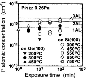
Figure 3. PH3 exposure time dependence of the P atomic concentration on Si(100) and on Ge(100).
![]() Atomic layer doping in Si and SiGe epitaxial growth
Atomic layer doping in Si and SiGe epitaxial growth
Atomic layer doping is performed by epitaxial growth over the material formed on Si(100) or SiGe(100) surface.4-7,16-19 The epitaxial growth of Si/0.5 AL of N/Si(100),5,17 Si/0.5 AL of P/Si(100),5,18 SiGe/1 AL of B/SiGe(100),7,16 SiGe/0.8 AL of C/SiGe(100),6 and Si/0.03 AL of W/Si(100)19 have been reported. In this section, we review the atomic layer doping of N, P and B.
In the case of Si/0.5 AL of N/Si(100) growth, the Si film is epitaxially grown by SiH4 exposure at 500 °C on the nitrided Si(100) surface formed by NH3 reaction at 400 °C. Most of the N atoms are buried in the initially nitrided region within the thickness of about 1 nm within the measurement accuracy, as shown in Fig. 4(a). It should be noted that N atoms tend to segregate at the grown surface with increasing Si growth temperature. If the N amount is 6×1014 cm−2, amorphous Si is grown, probably caused by the generation of Si3N4. We have achieved high-quality epitaxial growth of multi-layer N-doped Si films composed of 3×1014 cm−2 N layers and 3.0 nm thick Si spacers. In such N AL-doped Si films, the N atoms act as donors. The typical donor activation ratio is about 0.4% at the N amount in a 5×1013 cm−2/layer. Ionization energy of the donor level is about 150–180 meV. The Hall mobility is much larger than the ~100 cm2/V.s value expected at 300 K from uniformly P-doped Si with P concentration of 1019 cm−3, reaching instead values typical of 1016−1017 cm−3 bulk doping, see Fig. 4(b). Since the local concentration of the ionized donors is about 1018−1019 cm−3 in 1 nm-thick N doped region, we believe that scattering in electron transport is reduced by AL doping. Moreover, there is a possibility that the carrier mobility is enhanced by highly concentrated strain near the N AL-doped region. Since N atoms in delta-doped regions tend to diffuse and a part of them segregates at the surface at 750 °C, very low temperature subsequent processing is required for the device fabrication.

Figure 4. (a) Depth dependence of the N1s intensity measured by XPS and depth profile of N concentration for the AL-doped Si film with the 3×1014 cm−2 N concentration. The total N amount for the doped region is roughly 3×1014 cm−2. (b) Measured temperature dependence of electron Hall mobility in the N AL-doped Si films. Solid lines indicate Hall mobility of the bulk doped n-Si.20 Mobility of uniformly P-doped Si epitaxial film grown by LPCVD on Si(100) with 1019 cm−3 concentration is also shown for comparison (open diamond).
In the case of Si growth on the (100) surface with P amount of 2×1015 cm−2 at a SiH4 partial pressure of 6 Pa at 500 °C,18 the surface P concentration decreases with increasing SiH4 exposure time without Si deposition. After the P concentration falls below one AL due to the SiH4 reaction, Si growth begins and P atoms segregate onto the surface. As a result, AL P doping below 1014 cm−2 can be achieved in Si1−xGex epitaxial growth at above 500 °C by using reduced pressure CVD in a single wafer reactor.16 At a rather low temperature of 450 °C and a rather high SiH4 partial pressure of 220 Pa, P incorporation into the Si film and the growth of heavily P delta-doped Si film have been achieved without an incubation period of Si growth,18 although the tailing towards surface was also observed. The SiH4 reaction is suppressed in the P-doped Si deposition by using SiH4-PH3, but not by Si2H6-PH3.21 The Si2H6 is produced due to polymerization of SiH4 and increases in proportion to the square of the SiH4 partial pressure.22 In the case of 220 Pa partial pressure of SiH4, Si deposition may be enhanced by Si2H6 produced from SiH4, because almost no Si deposition is observed at a SiH4 partial pressure of 220 Pa. By this technique, heavily P-doped epitaxial Si films on Si(100) with average P concentration of 6×1020 cm−3 can be formed with 7 nm Si spacers, as shown in Fig. 5(a). The average carrier concentration reaches a value as high as 3.6×1020 cm−3 and the resistivity as low as 2.7×10⁻⁴ Ω·cm, as shown in Fig. 5(b).

Figure 5. (a) Depth profile of the P concentration in the four layers of P-doped epitaxial Si film measured by SIMS. Atomic amount of adsorbed P is 1.4×1015 cm−2 for each layer. For subsequent Si growth, the SiH4 partial pressure was 220 Pa and the temperature was 450 °C. (b) Annealing temperature dependence of carrier concentration and resistivity of the P-doped epitaxial Si films from the same batch as in (a); annealing time was 60 minutes.
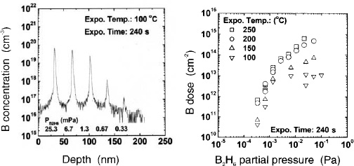
Figure 6. (a) SIMS profile of B peaks in Si0.8Ge0.2 grown at different B2H6 partial pressures during 240 s exposure at 100 °C in N2 (total pressure was 10640 Pa). (b) B dose in Si0.8Ge0.2 vs. B2H6 partial pressures for 240 s exposure between 100 and 250 °C (total pressure was 10640 Pa).
However. annealing the material above 550 °C causes a decrease in carrier concentration and an increase in resistivity. They become close to those of the P-doped Si film formed by P diffusion at 1000 °C.23 We believe that low-resistivity P-doped Si films result from a higher Si deposition rate that suppresses electrically inactive P formation mechanisms. such as P clustering. Using AL doping. a very low contact resistivity of about 5×10⁻⁸ Ω·cm−2 between Ti and the Si film has been obtained.25
Atomic level control of B doping of Si1-xGex and Si1-xGex:C films can also be obtained by reduced-pressure CVD in a single wafer reactor. At temperatures of 350 °C and higher,6,25 the B AL process is not self-limited. Boron atomic concentration incorporated into the SiGe epitaxial films (B dose) increases with increasing B2H6 partial pressure without saturation. and a B dose of several monolayers can be obtained.10 This also implies that B adsorption occurs at Si, Ge and B surface sites, consistent with the fact that B tends to form clusters in Si1-xGex at high B concentration.25 If the B dose is higher than one monolayer, B tends to be incorporated as electrically inactive. Figure 6(a) shows the secondary ion mass spectroscopy (SIMS) profile of B peaks fabricated at different B2H6 partial pressures at exposure temperature of 100 °C. To increase the B dose at this low temperature, the hydrogen termination of the Si surface was prevented by cooling down under N2 to 100 °C after the Si1-xGex epitaxy and performing the exposure at low temperature in N2.7 Very steep B profiles of 1 nm/decade have been obtained. Figure 6(b) shows the B dose as a function of the B2H6 partial pressure for different exposure temperatures. In contrast to the exposure at higher temperature, where no self-limitation is observed, there are indications of saturation at low temperature. By lowering the temperature of the adsorption step from 250 °C to 100 °C. saturation behaviour of the B dose at high B2H6 partial pressures is visible. The process tends to become self-limited at the lowest temperature used. Compared with the adsorption at higher temperature, the adsorption of B2H6 at Si and Ge sites seems to be favourable. As a result of this change in the adsorption mechanism, one would expect a higher proportion of electrically active B at very low temperatures.
3. Atomically controlled plasma processing
![]() Si and Ge epitaxial growth on Si(100) by ECR Ar plasma enhanced CVD
Si and Ge epitaxial growth on Si(100) by ECR Ar plasma enhanced CVD
Si and Ge epitaxial growth was performed using ultraclean ECR Ar plasma enhanced reaction without substrate heating. The system is schematically shown in Fig. 7(a).26-28 Argon plasma was generated by supplying microwave power (2.45 GHz) at Ar pressure of 2.1 Pa. For 200 W microwave power, flux density and peak energy of the incident Ar ions were about 3×1015 cm−2 s−1 and 2 eV, respectively, and substrate temperature was below 50 °C during the 10 minute plasma exposure. For 800 W microwave power, the corresponding values were 8×1016 cm−2 s−1 and 3 eV, respectively, and substrate temperature increased to above 300 °C at 10 minutes.26
Typical RHEED patterns of the deposited Si and Ge films are shown in Fig. 7(b). Clear streaks are observed. It should be noted that crystallinity degradation tends to proceed with incorporation of Ar atoms (above 2×1021 cm−3) in the deposited Si film.26 In the case of GeH4 reaction on Si(100) at lower microwave power, the deposited Ge film has an atomically flat surface with a roughness of about 0.1−0.2 nm. For the higher microwave power, the surface roughness is relatively larger. We believe the rough surface is due to the higher substrate temperature during the deposition.
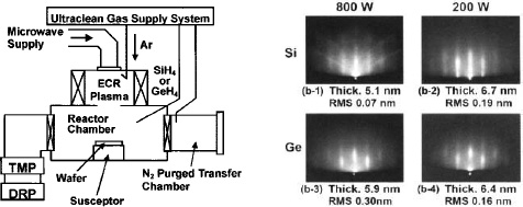
Figure 7. (a) Schematic diagram of an ultraclean ECR plasma enhanced CVD system (<10-5 Pa ultimate vacuum, TMP and DRP are turbomolecular and dry pumps). (b) RHEED patterns from [011] azimuth of Si and Ge films grown on Si(100). Thickness and root mean square (RMS) value of surface roughness are also shown.

![]() Atomic-order nitridution of Si(100) by ECR nitrogen plasma
Atomic-order nitridution of Si(100) by ECR nitrogen plasma
Atomic-order plasma nitridation of Si(100) was performed by ECR nitrogen plasma.29,30 Energy distribution, peak energy of the incident ions, flux density and relative optical emission intensity IN from the typical N2 radical (337.1 nm: C3Πu − B3Πg second positive system) are summarized in Table 2. The dependence of the N atomic concentration on the product of IN and plasma exposure time t is shown in Fig. 8. Below 1–2 AL the N concentration correlates with the JN × t product. Therefore, in the initial stages of nitridation, the N radicals are the major species to contribute to the plasma nitridation of Si. Assuming that the radicals react only with surface atoms and the reaction proceeds according to the Langmuir-type kinetics neglecting desorption, the N atomic concentration (nN) is given by:

Figure 8. Dependence of the N atomic amount on the product of the relative optical emission intensity IN and the plasma exposure time t. Dashed line corresponds to Eq. (1), 1 AL (6.78×1014 cm−2) and 2 AL (1.36×1015 cm−2) of Si(100) are also indicated.
where ns is the saturated N atomic amount, kN is reaction rate constant of the radicals, and α is the constant converting IN to number of the incident radicals. The broken line in Fig. 8 is obtained by fitting the experimental data to Eq. (l), where ns is set to 1.36×1015 cm−2 (2 AL). In all the cases, good agreement is observed in the initial nitridation region provided the substrate is cooled. Without cooling, the saturated N amount is over 2 AL, and deviates from Eq. (1). The deviation can be caused by contribution of the incident ions, because the incident ions are expected to react with deeper atoms below the surface.
![]() Epitaxial growth of N delta-doped Si films by ECR plasma enhanced CVD
Epitaxial growth of N delta-doped Si films by ECR plasma enhanced CVD
Atomic-order nitridation of Si(100) and subsequent Si epitaxial growth on the nitrided Si(100) were carried out without substrate heating. Argon and SiH4 were supplied into the plasma-generation and reactor chambers, respectively. Depth profiling of N and Ar concentrations was obtained from repeated XPS measurements combined with sub-nanometer wet etching. The results for Si epitaxial films deposited on the nitrided Si(100) are shown in Fig. 9.31 Most of the N atoms are confined to a roughly 3 nm thick region. Since peak position for the N concentration is shifted towards the Si capping layer, we believe N atoms tend to segregate during the Si deposition. The incorporated N atoms are confined to a 3 nm thick region and the total N dose reaches as high as 5.5×1014 cm−2 (0.8 AL). This amount is much larger than the value obtained by the thermal CVD described above. The Ar concentration peak shifts further than the N concentration peak, and the incorporated Ar dose is much lager than that for a Si film without N doping.

Figure 9. Depth profile of N and Ar concentration for the Si epitaxial film deposited on the 7.6×1014 cm−2 (1.1 AL) nitrided Si(100). Bottom pictures are RHEED patterns taken from (a) the deposited Si film surface and (b) the partially etched surface at a depth of 6.8 nm.
4. Conclusions
Self-limiting formation of 1–3 atomic layers of group IV or related atoms by thermal adsorption and reaction of hydride gases on Si(100) and Ge(100) is generalized based on a Langmuir-type model. Atomic layer doping of N, P and B can be achieved by the epitaxial growth of Si and SiGe over the material formed on (100) surfaces. Atomic layer doping results indicate that new group IV semiconductors of very high carrier concentration and higher mobility can be prepared compared to doping under equilibrium conditions. Our results indicate that atomic layer-by-layer epitaxy of group IV materials as well as atomic layer doping are possible with well-controlled initiation of the reaction governed by Langmuir-type self-limited kinetics in many cases, and open the way to atomically controlled CVD technology for ULSI.
By using ECR Ar plasma-enhanced CVD, Si and Ge epitaxial growth from SiH4 and GeH4, respectively, are achieved on Si(100) without substrate heating. Results of nitrogen plasma irradiation of Si(100) suggest that the nitridation of the Si atoms below the surface is enhanced with increasing ion energy as well as the Si surface temperature. Silicon epitaxy on atomic-order nitrided Si(100) can also achieved without substrate heating, with the result that about 0.8 atomic layers of N can be confined within an approximately 3 nm thick region. These results open the way to room-temperature atomically controlled processing.
References
- B. S. Meyerson, “Low-temperature silicon epitaxy by ultrahigh vacuum/chemical vapor deposition,” Appl. Phys. Lett. 48, 797 (1986).
- J. Murota, N. Nakamura, M. Kato, N. Mikoshiba, and T. Ohmi, “Low-temperature silicon selective deposition and epitaxy on silicon using the thermal decomposition of silane under ultraclean environment,” Appl. Phys. Lett. 54, 1007 (1989).
- J. Murota and S. Ono, “Low-temperature epitaxial growth of Si/Si1-xGex/Si heterostructure by chemical vapor deposition,” Jpn. J. Appl. Phys. 33, 2290 (1994).
- J. Murota, T. Matsuura, and M. Sakuraba, “Atomically controlled processing for group IV semiconductors,” Surf. Interface Anal. 34, 423 (2002).
- J. Murota, M. Sakuraba, and B. Tillack, “Atomically controlled processing for group IV semiconductors by chemical vapor deposition,” Jpn. J. Appl. Phys. 45, 6767 (2006).
- B. Tillack, B. Heinemann, and D. Knoll, “Atomic layer doping of SiGe – Fundamentals and device applications,” Thin Solid Films 369, 189 (2000).
- B. Tillack, Y. Yamamoto, D. Bolze, et al., “Atomic layer processing for doping of SiGe,” Thin Solid Films 508, 279 (2006).
- D. Lee, S. Takehiro, M. Sakuraba, J. Murota, and T. Tsuchiya, “Fabrication of 0.12- m pMOSFETs on high Ge fraction Si/Si1-xGex/Si(100) heterostructure with ultrashallow source/drain formed using B-doped SiGe CVD,” Appl. Surf. Sci. 224, 254 (2004).
- R. Banisch, B. Tillack, M. Pierschel, K. Pressel, R. Barth, D. Krüger, and G. Ritter, “A novel infrared SiGe/Si heterojunction detector with an ultrathin phosphorus barrier grown by atomic layer deposition,” Proc. MRS Symp. 450, 213 (1997).
- B. Tillack, Y. Yamamoto, D. Knoll, B. Heinemann, P. Schley, B. Senapati, and D. Krüger, “High performance SiGe:C HBTs using atomic layer base doping,” Appl. Surf. Sci. 224, 55 (2004).
- M. Sakuraba, T. Matsuura, and J. Murota, “H-termination on Ge(100) and Si(100) by diluted HF dipping and by annealing in H2,” in: J. Ruzyllo and R. E. Novak, eds., Proc. 5th Intern. Symp. Cleaning Technol. Semicond. Dev. Manufact., Pennington, NJ: The Electrochemical Society, 1997, p. 213.
- T. Watanabe, M. Sakuraba, T. Matsuura, and J. Murota, “Atomic-layer surface reaction of SiH4 on Ge(100),” Jpn. J. Appl. Phys. 36, 4042 (1997).
- A. Izena, M. Sakuraba, T. Matsuura, and J. Murota, “Low-temperature reaction of CH4 on Si(100),” J. Crystal Growth 188, 131 (1998).
- T. Takatsuka, M. Fujiu, M. Sakuraba, T. Matsuura, and J. Murota, “Surface reaction of CH3SiH3 on Ge(100) and Si(100),” Appl. Surf. Sci. 162-163, 156 (2000)
- Y. Shimamune, M. Sakuraba, T. Matsuura, and J. Murota, “Atomic-layer adsorption of P on Si(100) and Ge(100) by PH3 using an ultraclean low-pressure chemical vapor deposition,” Appl. Surf. Sci. 162-163, 388 (2000).
- B. Tillack, “Atomic control of doping during SiGe epitaxy,” Thin Solid Films 318, 1 (1998).
- Y. Jeong, M. Sakuraba, and J. Murota, “Electrical properties of N atomic layer doped Si epitaxial films grown by ultraclean low-pressure chemical vapor deposition,” Mater. Sci. Semicond. Process. 8, 121 (2005).
- Y. Shimamune, M. Sakuraba, J. Murota, and B. Tillack, “Formation of heavily P-doped Si epitaxial film on Si(100) by multiple atomic-layer doping technique,” Appl. Surf. Sci. 224, 202 (2004).
- T. Kurosawa, T. Komatsu, M. Sakuraba, and J. Murota, “Electrical properties of W delta-doped Si epitaxial films grown on Si(100) by ultraclean low-pressure chemical vapor deposition,” Mater. Sci. Semicond. Process. 8, 125 (2004).
- S. S. Li and W. R. Thurber, “The dopant density and temperature dependence of electron mobility and resistivity in n-type silicon,” Solid State Electronics 20, 609 (1977).
- S. Nakayama, H. Yonezawa, and J. Murota, “Deposition of phosphorus doped silicon films by thermal decomposition of disilane,” Jpn. J. Appl. Phys. 23, L493 (1984).
- T. Morie and J. Murota, “Trench coverage characteristics of polysilicon deposited by thermal decomposition of silane,” Jpn. J. Appl. Phys. 23, L482 (1984).
- R. B. Fair and J. C. C. Tsai, “A quantative model for the diffusion of phosphorus in silicon and the emitter dip effect,” J. Electrochem. Soc. 124, 1107 (1977).
- J. Noh, M. Sakuraba, J. Murota, S. Zaima, and Y. Yasuda, “Contact resistivity between tungsten and impurity (P and B)-doped Si1-x-yGexCy epitaxial layer,” Appl. Surf. Sci. 212-213, 679 (2003).
- B. Tillack, P. Zaumseil, G. Morgenstern, D. Krüger, and G. Ritter, “Strain compensation in Si1-xGex by heavy boron doping,” Appl. Phys. Lett. 67, 1143 (1995).
- D. Muto, M. Sakuraba, T. Seino, and J. Murota, “Argon plasma irradiation effects in atomically controlled Si epitaxial growth,” Appl. Surf. Sci. 224, 210 (2004).
- K. Sugawara, M. Sakuraba, and J. Murota, “Atomically controlled Ge epitaxial growth on Si(100) in Ar-plasma-enhanced GeH4 reaction,” Mater. Sci. Semicond. Process. 8, 69 (2005).
- K. Sugawara, M. Sakuraba, and J. Murota, “Thermal effect on strain relaxation in Ge films epitaxially grown on Si(100) using ECR plasma CVD,” Thin Solid Films 508, 143 (2006).
- T. Seino, T. Matsuura, and J. Murota, “Contribution of radicals and ions in atomic-order plasma nitridation of Si,” Appl. Phys. Lett. 76, 342 (2000).
- T. Seino, D. Muto, T. Matsuura, and J. Murota, “Thermal effects in atomic-order nitridation of Si by a nitrogen plasma,” J. Vac. Sci. Technol. B 20, 1431 (2002).
- M. Mori, T. Seino, D. Muto, M. Sakuraba, and J. Murota, “Si epitaxial growth on atomic-order nitrided Si(100) using electron cyclotron resonance plasma,” Mater Sci Semicond. Process. 8, 65 (2005).