
Merging Nanoepitaxy and Nanophotonics
Institut für Festkörperphysik
Tech. Univ. Berlin, D-10623 Berlin, Germany and
Abraham Ioffe Physical Technical Institute, St. Petersburg, Russia
Institut für Festkörperphysik
Tech. Univ. Berlin, D-10623 Berlin, Germany
1. Introduction
Nanostructures are rapidly penetrating optoelectronic devices, enabling novel active media concepts and operation principles. Applications of nanostructures occurs in the three main directions: nanoepitaxy, nanophotonics and novel functionality. Nanoepitaxy utilizes growth-related phenomena at the nanoscale level, including self-organized formation and control of epitaxial nanostructures, and techniques of defect reduction and defect engineering. Nanophotonics addresses modification of the key optical properties by advanced epitaxial design and/or lateral patterning of the surfaces and interfaces with nanoscale resolution. Novel functionality enables control over performance of nanophotonic devices by utilizing optical interference phenomena controlled by electrooptic effects. In this chapter we give an overview of recent results, concentrating on all-epitaxial approaches aimed at realizing a broad range of novel devices, as opposed to widely discussed nanoscale patterning concepts addressed in other chapters of this volume.
2. Nanoepitaxy: Self-organized growth of low-dimensional structures
Nanoepitaxy utilizes effects of spontaneous formation of ordered nanostructures at crystal surfaces1 and can result in quantum wires, quantum dots (QDs) or vertical quantum well structures.2 The key processes are: spontaneous formation of three-dimensional (3D) islands in lattice-mismatched growth, spontaneous surface periodic nanofaceting, and spontaneous lateral alloy phase separation into ordered nanodomains. These approaches are schematically presented in Fig. 1 and all are applied to the field of active media for advanced devices. The first lasing action in self-organized QDs was demonstrated in 1993.3
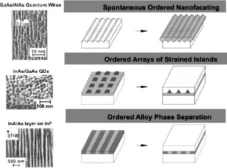
Figure 1. Schematic representation of the three key approaches to spontaneous formation of nanostructures at crystal surfaces (from Ref. 1).
![]() Quantum wire devices
Quantum wire devices
Quantum well wire (QWW) structures are formed when growth takes place on nanofaceted or step-bunched surfaces.1,2 It is well established that some high-index crystal planes with a high surface energy can be unstable with respect to spontaneous 1D or 2D nanofaceting, so ordered nanofaceting provides an energetically favorable state. Vicinal surfaces are also well known to undergo a transition to step bunching, with a characteristic example of a GaAs (100) surface misoriented by 10° towards the main diagonal direction, being effectively a high-index GaAs (![]() ) surface. These substrates are broadly used for growth of (In,Ga,Al)P lasers for optical storage and display applications (620–660 nm). Elastic strain relaxation at the edges of the faceted surface enables alloy phase separation and spontaneous formation of natural superlattices during growth. A schematic representation of the growth mechanism is presented in Fig. 2.
) surface. These substrates are broadly used for growth of (In,Ga,Al)P lasers for optical storage and display applications (620–660 nm). Elastic strain relaxation at the edges of the faceted surface enables alloy phase separation and spontaneous formation of natural superlattices during growth. A schematic representation of the growth mechanism is presented in Fig. 2.
Phase separation is a well-studied phenomenon in ternary and quaternary (In,Ga,Al)P layers. It originates from the intrinsic strain-stabilization mechanism in III-V alloys. Once the strain can relax at surface steps or step bunches, the alloys tend to separate into phases. To prevent growth-related instabilities resulting in bandgap and effective mass modulation across the layer, a significant surface misorientation of the GaAs substrate with respect to the exact (100) direction is used to control the phase separation effect and prevent formation of macroscopic domains.
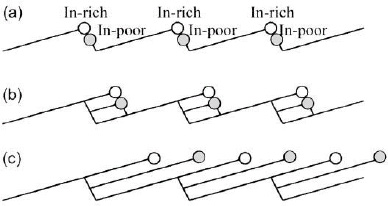
Figure 2. Schematic representation of epitaxial growth of an alloy layer on top of a step-bunched GaAs surface. Surface corrugation leads to the formation of a natural tilted superlattice.

Figure 3. Natural superlattice formed by (In,Ga,Al)P layer growth on a step-bunched GaAs(100) surface misoriented by 10° towards <111>.
In Fig. 3 we show transmission electron microscopy (TEM) images of an (In,Ga,Al)P cladding layer of a DVD laser lattice-matched to the GaAs substrate. The images are taken in the direction parallel (a) and perpendicular (b) to the step bunches. From the vertical periodicity of the natural superlattice (~5–6 nm) one can extract the expected lateral periodicity of the step-bunched surface of ~30–35 nm. The interface between the (In,Ga,Al)P layer and an (In,Ga)P layer grown on top of it is shown in Fig. 4. One can see that, indeed, the lateral periodicity falls in the range expected from the stripe pattern revealed in the TEM images of Fig. 3. Introduction of strain affects the lateral periodicity and the material distribution within the active region of the DVD laser diode.
To observe the structure of the active region of the DVD laser in detail, cross–section high-resolution TEM (HRTEM) studies have been performed. Figure 5(a) demonstrates the HRTEM image in the (![]() ) cross-section.
) cross-section.
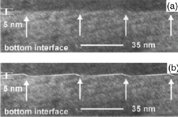
Figure 4. Natural superlattice formed by (In,Ga,Al)P and a corrugated interface (In,Ga,Al)P/InGaP formed by growth on a step-bunched GaAs surface.

Figure 5. HRTEM and processed HRTEM images revealing interface corrugation of the active layers in the direction perpendicular to the step bunches.
The processed HRTEM image in Fig. 5(b) yields the lattice-mismatch map, where the gray scale is used to encode the lattice mismatch. Darker regions correspond to a smaller mismatch with respect to the substrate, e.g. regions with a lower In content, whereas brighter regions correspond to a larger mismatch with respect to the substrate, e.g. regions with a higher In composition. Figure 5(b) reveals planar interface structures, as it is taken perpendicular to the step bunches. In this direction the corrugation causes only broadening of the contrast and, thus, overestimated thickness is observed. In contrast, the image taken in the direction perpendicular to step bunches reveals the lateral periodicity of the corrugation of ~25 nm and a height of ~3 nm. The modification of the surface nanofaceting can be attributed to the renormalization of the surface energy by external strain resulting in a different equilibrium geometry of the faceted surface.1,4
The amplitude of the lattice mismatch modulation is about 3%, which corresponds to the variations of In content from 49% (barriers lattice-matched to the substrate) to 94% (local InGaP active layer regions that are close to pure InP). Thus, on top of interface corrugation, a dramatic alloy phase separation takes place, resulting in a quantum wire-like structures with a strong lateral confinement.
In Fig. 6 we show polarized luminescence spectra recorded from the heterostructure surface for directions parallel and perpendicular to the corrugation direction. One can see that the luminescence is predominantly polarized in the direction parallel to the corrugation direction, as expected for heavy-hole-like transitions. It follows from Fig. 6 that the degree of polarization approaches ~15% for the high-energy side of the luminescence spectrum, where the disorder-related effects are less important.
Interface and compositional modulations are particularly important for brightred lasers for display and DVD applications, as the devices operate at wavelengths close to the Γ to X conduction band transition and a strong mixing between the states is needed to achieve efficient luminescence at the transition point.5,6

Figure 6. Room-temperature polarized surface photoluminescence spectrum of the active region of a DVD laser. Note the significant degree of polarization.
The next generation of lasers for optical storage is based on InGaN lasers in the violet (~410 nm). The InGaN light-emitting devices are also advantageous as sources for blue and green emission for projection displays. A unique property of these devices is spontaneous formation of InN-rich nanodomains (see Fig. 7), whose density and size increase dramatically as the substrate temperature is decreased. Evidence of QD-like InGaN structural and electronic properties was reported in a number of publications.1,7-10 It was, for example, observed that when the luminescence spectra are recorded from small openings in metal masks, a broad spectrum of InGaN emission splits into discrete ultranarrow lines with a density corresponding to the density of quantum dots revealed in the HRTEM studies.9
Experiments also confirmed lack of lateral transport even at nanoscale dimensions of the openings. Resonant excitation along the contour of the InGaN luminescence band revealed the resonant nature of the resulting emission, with no significant spectral diffusion even after a long delay (>10 ns) after the excitation pulse.10 Localization of carriers in InGaN QDs is a key requirement to achieve high degradation robustness of light-emitting diodes and lasers.
Quantum dot lasers based on InGaAs material system are also quickly progressing. High-power operation and long operating lifetimes, as well as ultrahigh-speed temperature-insensitive operation have been reported.11 Lasers at 1300 nm with expected lifetime exceeding 106 hours at 40° heat sink temperature and 50 mW cw single-mode operation have been demonstrated.11,12 Aging tests of the 1300 nm-range QD lasers are presented in Fig. 8. No sudden failure was observed and no laser reached the failure criterion (–20% of initial power) during a >2000 hour test. Stable spectral width and absence of any blue shift of the lasing wavelength are evidence of robustness of the QD region against In-Ga intermixing.
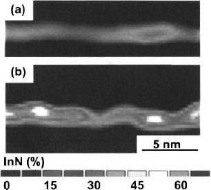
Figure 7. A grayscale map of InN distribution within an InGaN insertion in a GaN matrix, grown at 785 °C (a) and 755 °C (b), respectively. The dot size and density increase with a decrease in substrate temperature.
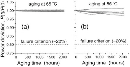
Figure 8. Output power vs. aging time at 65 °C(a) and 85 °C (b).
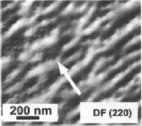
Figure 9. TEM image of low InAs composition InGaAs QDs formed in a submonolayer deposition mode.
Quantum dot 1300 nm lasers proved to be suitable for 10 GHz fully temperature-insensitive operation (20–70 °C) and enabled 5–100 GHz ultrashort-pulse temperature-robust mode locking and, also, distortion-free amplification of optical signals at 100 GHz and above.12
An important technique for QD formation is submonolayer growth, where QDs are “stacked” with a seed layer formed by submonolayer (SML) InAs deposition. This technique enables formation of QDs even in the case of relatively low average InAs composition in the insertion. A plan-view TEM image of such a structure is shown in Fig. 9.13
Submonolayer QDs can be successfully applied to conventional 800–1100 nm edge- and surface-emitting lasers, improving temperature performance, speed and degradation robustness. Ultrahigh temperature stability and ultrahigh-speed SML QD VCSELs are presented in Fig. 10.13
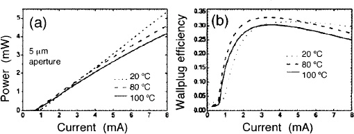
Figure 10. High-temperature performance of continuous wave 980 nm VCSELs based on submonolayer quantum dots.

Figure 11. (a) Eye diagram for 20 GB/s NRZ 27-1 PRBS of a 6 μm SML QD VCSEL at 25 and 85 °C without change of the bias current and modulation voltage. (b) Bit-error-rate (BER) at 20 Gb/s with 27-1 PRBS at 25 and 85 °C for the same bias current.
Directly-modulated continuous wave SML QD VCSELs grown in the anti-waveguiding design13,14 have demonstrated >20 Gb/s modulation in the 20–85°C temperature range. No adjustment of the modulation current and voltage was applied, as shown in Fig. 11. Furthermore, relaxation oscillation frequency of 28 GHz indicated potential to reach 40 Gb/s direct modulation with further design optimization.
3. Nanoepitaxy: Defect reduction
In this section we discuss the defect reduction (DR) advantages of nanoepitaxy.
![]() Defect reduction in quantum dots
Defect reduction in quantum dots
Self-organized formation of QDs results in characteristic QD size and shape dispersion of typically 10–20%. Steps, defects, and impurities on the surface may stimulate formation of large, plastically relaxed islands, which degrade the device performance and reduce operating lifetime. In the 1970’s and early 1980’s, it was generally assumed that 3D InAs islands on GaAs15,16 are severely dislocated.16,17 It was therefore assumed that one had to avoid islands to obtain structurally perfect devices.17
Formation of dislocated InAs islands can be avoided, however, by proper adjustment of growth conditions and the InAs layer thickness.18,19 For longer wavelength InAs QDs of larger sizes, this adjustment becomes increasingly difficult. For example, it was found that InAs/GaAs QDs formed at low substrate temperature may represent chains of laterally merged InAs islands emitting up to 1700 nm.1 However, most of these objects are dislocated, resulting in extremely low integrated luminescence efficiency at room temperature. A possible way to remove the large dislocated islands is to use relatively thin GaAs caps to ensure that highly dislocated QDs remain uncapped. Then, growth interruption at high substrate temperature causes selective evaporation of uncapped InAs islands due to much higher temperature stability of GaAs.20 At the same time, small dislocated islands may also exist. These islands, however, impose a different strain field in the GaAs cap layer after overgrowth, as compared to coherent QDs. Depositing an AlAs layer and annealing at an even higher temperature, high enough to enable GaAs evaporation (Fig. 12), leads to a drastic reduction in defect density and dramatic improvement in photoluminescence efficiency.21
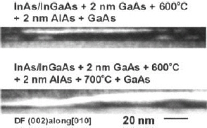
Figure 12. Cross-sectional TEM of InAs/InGaAs QDs emitting at 1.3 μm. The QDs are capped with 2 nm of GaAs, a 10 minute anneal at 600 °C is performed, then a 2 nm AlAs cap is deposited, followed by an additional 1 min anneal at 700 °C (bottom) before the GaAs overgrowth. AlAs deposition leaves detective QDs uncapped due to higher mismatch; they can be selectively removed by a 700 °C anneal.
The concept of defect reduction can be further extended to layered structures containing both misfit and threading dislocations and to fabrication of thick defectfree layers.22,23
Misfit dislocations cause strain due to a missing (or additional) crystal plane originating at the epilayer interface in order to accommodate the lattice mismatch. As a result, the InGaAs dislocated layer becomes nonuniformly strained in the regions between the misfit dislocations. This causes a repulsive interaction between the GaAs/AlAs cap layer and the dislocated region (the effect opposite to the alignment of InAs QDs in stacked rows). Uncovered dislocated regions may be selectively removed by annealing, which does not affect the AlAs-capped regions24 resulting in coherent nanopatterned epitaxial structures.

Figure 13. Schematic presentation of threading dislocations at the surface and their agglomerates.
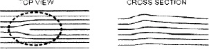
Figure 14. Surface morphology modulation in the vicinity of a threading dislocation.
Improved understanding of QD formation and defect removal stimulated work devoted to blocking the threading dislocations originating in thick epitaxial layers grown on top of lattice-mismatched substrate.
In the case of threading dislocations, additional lattice planes penetrate into the crystal, as shown in Fig. 13, and cause local strain fields in the vicinity of the exit point of the dislocation at the surface, as shown in Fig. 14. These defects can be fully removed by annealing only if they are correlated, as shown schematically in Fig. 13. Also, nanopipe defects in GaN, dislocation loops, local domains and nanoinclusions can be completely removed in certain cases.
For threading dislocations the most effective way of blocking them is their tilting towards in-plane penetration by selective annealing and overgrowth. Vertically propagating threading dislocations are driven by an underlying strain field, analogously to the vertically-correlated growth of strained quantum dots. In the case when this strain correlation can be removed and the growth front asymmetry is applied, bending of the dislocation becomes the most likely scenario.
Figure 15. Surface morphology modulation at the vicinity of threading dislocation.
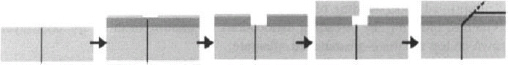
Figure 16. Schematic representation of possible routes of the defect reduction technique in case of a single threading dislocation.
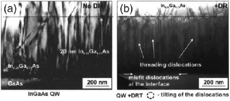
Figure 17. Cross-sectional TEM images illustrating defect reduction in an InGaAs layer grown on top of GaAs substrate at 500 °C. Annealing after 20 nm In0.35Ga0.65As QW layer growth was not applied (a) or applied (b). One can see that annealing dramatically enhances the probability of dislocation tilting. The QW layer position is indicated by a dashed line.
In Figs. 15 and 16 we show a schematic representation of the effect of annealing on the defective region. Formation of nanovoids may occur,26 further assisting the DR procedure. An example of applying the DR technique to In0.3Ga0.7As epitaxial layers deposited at 500 °C on GaAs is shown in Fig. 17.
One can see that the efficiency of the procedure is very high and practically all the dislocations are tilted after its application. The tilted dislocations may annihilate much more effectively in the upper layers. Furthermore, the tilt angle may be enhanced by multiple application of the DR procedure, leading to a complete in-plane blocking of the dislocation. Thus, InGaAs buffers grown at lower temperatures demonstrate lower density of threading dislocations, as shown in Fig. 18, which also illustrates the blocking of dislocations.25
A similar approach can be applied to epitaxial growth of GaN on sapphire and other substrates.25 In Fig. 19 we show defect blocking in GaN epitaxial layers, enabled by the defect reduction technique. We believe that further development of DR may also result in dramatic improvements in crystalline perfection of III-V epilayers grown on Si and other foreign substrates.
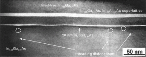
Figure 18. Cross-sectional TEM image illustrating application of the defect reduction technique to metamorphic heavily dislocated InGaAs layers grown on GaAs at 450 °C. In-plane blocking of dislocations is shown by circles.
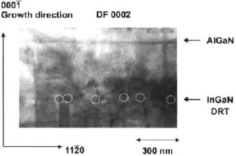
Figure 19. Cross-section TEM image illustrating application of DR to GaN epilayer on sapphire. Note in-plane blocking of threading dislocations at the DR regions.
![]() Degradation robustness of metamorphic lasers
Degradation robustness of metamorphic lasers
Metamorphic (MM) QD lasers on GaAs are attractive for long-wavelength applications (1.4–3 μm), including VCSELs. Recently, edge-emitting QD lasers emitting near 1.5 μm demonstrated output power up to and above 7 W with high differential efficiency (>50%).27 At high temperatures, the lasing wavelength was approaching ~1.52 μm. In Fig. 20 we show plan-view and cross-sectional TEM images of metamorphic 1500 nm QDs used in MM lasers. Narrow stripe lasers demonstrating cw 200 m W single-mode operation have also been realized.
The MM laser heterostructure studied for degradation robustness was grown at 450°C using elemental source molecular beam epitaxy (MBE) on Si-doped GaAs (100) substrate. The active region, consisting of 10 layers of InAs self-organized QDs, was placed in the middle of an InxGa1-xAs (x ~ 0.21) waveguide with a thickness of 0.8 μm. Each layer of QDs was overgrown by a thin InyGa1-yAs (y ~ 0.41) layer. The MM buffer consisted of a 1 μm thick InGaAs layer, followed by n-type cladding InAlGaAs layer (Al ~ 0.3) with a thickness of 1.5 μm.
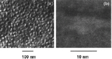
Figure 20. Plan-view (a) and cross-section (b) TEM images of InAs QDs inserted into a metamorphic In0.2Ga0.8As layer on a GaAs substrate.
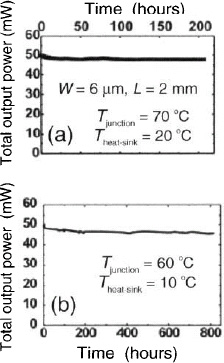
Figure 21. Degradation stability of long-wavelength MM lasers with as-cleaved facets vs. operation time, at 70 °C (a) and 60 °C (b) junction temperature. No significant degradation is been observed.
Aging tests at 60 °C junction temperature (10 °C heat sink temperature) of several as-cleaved devices with a cavity length L = 2 mm were performed in the current-stabilized mode, see Fig. 21. The initial total cw output power was about 50 mW. During the first 20 hours lasers showed a burn-in effect, and the output power decreased by about 5%. After aging tests lasting >800 hours of cw operation at this power, the lasers showed nearly no degradation in the performance. Aging tests at 70 °C junction temperature (20 °C heat sink) of similar devices showed no measurable degradation after >200 hours.28,29
4. Nanophotonics
Novel applications based on nanophotonics using the all-epitaxial growth approach have been proposed recently. The combination of light refraction, reflection, and interference enables efficient light-wave engineering of tilted optical modes. Ultimate control over the beam quality and emission wavelength in planar waveguides became possible. In this section, we will discuss two device classes: photonic band crystal (PBC) lasers and tilted cavity lasers (TCLs).
![]() Photonic band crystal laser
Photonic band crystal laser
The PBC laser, illustrated in Fig. 22, utilizes the filtering properties of multilayered media at a tilted angle of penetration with respect to the layer planes (longitudinal PBC effect).30,31 The small but finite vertical component of the k- vector of the in-plane optical mode can be properly engineered to enable dramatic discrimination of the excited optical modes through leakage loss and the boundary conditions at the multilayer filter-substrate interface. As a result, ultrahigh performance lasers emitting in the 640–650 nm range having a vertical beam divergence (full width at half maximum, FWHM) of only ~8 degrees can be fabricated. We have demonstrated 20 W pulsed power at 85% differential efficiency in 100 μm wide devices.32 Continuous wave single-mode operation in 4 μm wide stripes resulted in ~150 mW output power in devices without facet passivation, limited by catastrophic optical mirror damage (COMD).33
More recently, high power PBC lasers emitting at 850 nm have been fabricated.34 Devices based on 2 μm wide stripe geometry with facet passivation demonstrated above 160 mW cw operation at 20 °C heat sink temperature, still limited by COMD. It is important to note that the broadening of the waveguide suppresses both lateral modes and beam filamentation, enabling ultrahigh-power single mode lasers.
Further reduction of the vertical far field is possible. We have realized devices emitting in the 920–940 nm range with a FWHM of the vertical far field as narrow as ~4 degrees, as shown in Fig. 22(c). Single-mode 5 μm wide and 1.5 mm long stripe geometry devices demonstrated >500 mW cw power with a round-shape beam (~4°×4°).
The longitudinal PBC concept can be applied in 2D laser arrays and VCSELs and, also, utilized in light emitting diodes.

Figure 22. Conventional (a) and PBC (b) lasers. Note the multilayer waveguide region in (b), enabling stable spot size and a narrow far-field pattern. Vertical far field of the device emitting at 940 nm vs. angle ![]() is shown in (c).
is shown in (c).
![]() Tilted cavity laser
Tilted cavity laser
To address the problem of high-power wavelength-stabilized laser, the tilted cavity concept has been proposed.30,35 A tilted cavity laser (TCL) is another realization of an all-epitaxial nanophotonic structure, where lasing occurs in a high-order vertical optical mode. The value of the lasing mode angle is intermediate between the mode angle of a typical edge-emitting laser and the mode angle of a typical VCSEL. Such laser can operate in both edge-emitting and surface-emitting geometries. A TCL operating in edge-emitting geometry combines advantages of an edge emitter (high power operation) and a surface emitter (wavelength stabilization at any requested power).
A typical edge-emitting TCL contains a photonic band crystal that plays the role of a multilayer interference reflector (MIR) and an optical defect localizing the optical mode. The defect plays a role of a high-finesse cavity. To illustrate the principles of operation of a TCL it is convenient first to separately examine the optical properties of two key elements:30,35,36 the cavity, shown in Fig. 23(a), and the MIR, shown in Fig. 23(b).
Let us consider the reflectivity spectra of these two elements at oblique or tilted incidence of light, where we assume that light impinges on the element from a reference medium, and a semi-infinite GaAs substrate lies below. The cavity is basically a layer with a high refractive index sandwiched between two low-index layers. Figure 23(c) shows the reflectivity spectra of the cavity at three tilt angles ![]() . Each spectrum contains a dip that shifts quickly as a function of
. Each spectrum contains a dip that shifts quickly as a function of ![]() . Figure 23(d) depicts the reflectivity spectra of the MIR at the same three
. Figure 23(d) depicts the reflectivity spectra of the MIR at the same three ![]() . Each spectrum contains a stopband, which shifts slowly as a function of
. Each spectrum contains a stopband, which shifts slowly as a function of ![]() .
.
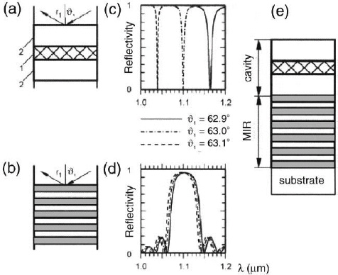
Figure 23. Principles of the wavelength selectivity in a tilted cavity laser (TCL): (a) cavity sandwiching a high refractive index layer between two low-index layers; (b) multilayer interference reflector (MIR); (c) reflectivity spectra of the cavity at three tilt angles ![]() ; (d) reflectivity spectra of the MIR at the same three tilt angles
; (d) reflectivity spectra of the MIR at the same three tilt angles ![]() ; (e) schematic structure of a TCL.
; (e) schematic structure of a TCL.
Figure 24(a) shows the angular dependence of the two features of the tilted cavity structure, namely the reflectivity dip of the cavity and the stopband maximum of the MIR. Most important is that these two features shift at different rates as a function of tilt angle ![]() . Therefore the cavity and the MIR can be intentionally designed such that the spectral position of the cavity dip and the MIR stopband reflectivity maximum coincide only at a certain angle
. Therefore the cavity and the MIR can be intentionally designed such that the spectral position of the cavity dip and the MIR stopband reflectivity maximum coincide only at a certain angle ![]() 0, and draw apart as the angle deviates from
0, and draw apart as the angle deviates from ![]() 0. Then the optical mode propagating at this angle
0. Then the optical mode propagating at this angle ![]() 0 is strongly confined within the cavity and only weakly transmitted through the MIR. As the angle deviates from the optimum value, the wavelength of the optical mode shifts away from the MIR stopband reflectivity maximum, the transmission of the MIR increases and the optical mode starts leaking out of the structure, either into the substrate or into the top contact.
0 is strongly confined within the cavity and only weakly transmitted through the MIR. As the angle deviates from the optimum value, the wavelength of the optical mode shifts away from the MIR stopband reflectivity maximum, the transmission of the MIR increases and the optical mode starts leaking out of the structure, either into the substrate or into the top contact.
In other words, the optical mode of a tilted cavity structure at the optimum wavelength λ0 should have a very low leakage loss, whereas the leakage loss will dramatically increase as the wavelength deviates from the optimum value. This promotes the wavelength selective operation of the laser. Moreover, the thermal shift of the optimum wavelength is governed by the temperature dependence of the refractive indices, like in VCSELs, rather than by the thermal shift of the electronic bandgap energy, like in conventional edge emitters. This feature of the device combines the advantages of the VCSEL and the edge emitter, resulting in a highpower wavelength-stabilized laser. The first experimental studies of the TCLs36,37 have confirmed the wavelength stabilization and a reduced thermal shift of the lasing wavelength with respect to conventional edge emitters. In particular, a GaAs/GaAlAs TCL with strained GaInAs quantum wells operating around 980 nm exhibited a 0.2 nm/K thermal shift of the lasing wavelength, as opposed to the 0.4 nm/K value for conventional edge-emitting lasers.

Figure 24. Optimum wavelength of a tilted cavity laser (TCL) and its thermal dependence. (a) Intersection of the angular dependences of the optical features of the cavity and MIR determines the lasing wavelength λ0 of a TCL. A weak thermally-induced red shift of the cavity produces a red shift of λ0 (b), whereas a strong red shift of the cavity produces a blue shift of λ0 (c).
Figure 24(b) illustrates the origin of the thermal shift in the TCL optimum wavelength. As the refractive indices of semiconductor materials increase with temperature, all curves shift to longer wavelengths. The intersection curve in Fig. 24(b) shifts to larger angles and to longer wavelengths as well, as expected.
However, a possibility of controlling the thermal shift34 is based on the strongly nonlinear behavior of the refractive index temperature coefficient dn/dT in semiconductor alloys. The temperature coefficient increases dramatically as the photon energy approaches resonance with the bandgap energy of the semiconductor. In GaAlAs alloys, the thermal coefficient dn/dT is especially high for GaAs. Then it is possible to replace, say, in one cavity layer, a homogeneous GaAlAs layer by a superlattice consisting of alternating layers of GaAlAs with a higher Al content and pure GaAs, such that the averaged refractive index at room temperature remains the same, and the temperature coefficient dnav/dT is much larger. As a result, the curve (dip position vs. angle) for the cavity will shift at an elevated temperature to much longer wavelengths, i.e. will exhibit a much stronger red shift, as shown in Fig. 24(c). As the dependence of the stopband maximum reflectivity of the MIR vs. tilt angle remains the same, the intersection point will be shifted to larger angles. Such shift can eventually become so large, that the intersection at an elevated temperature will occur at a shorter wavelength λ0’ < λ0. The corresponding superlattice in the cavity plays a role of the control element, allowing tuning of the thermal shift of λ0.

Figure 25. Temperature dependence of the leakage loss spectrum of a tilted cavity laser with three different realizations of the control element of the cavity at T = 300 (solid lines) and 400 K (dashed lines): (a) red shift of the loss minimum; (b) temperature independence of the loss minimum; (c) blue shift of the loss minimum.
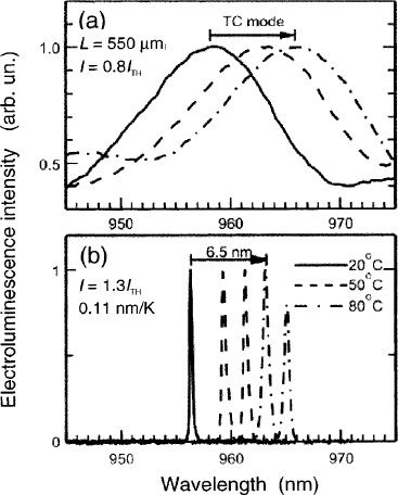
Figure 26. Thermal shift of the electroluminescence spectra (a) and lasing spectra (b) in a tilted cavity laser (TCL) using a GaAs/GaAlAs superlattice in the cavity.
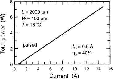
Figure 27. High-power operation of a tilted cavity laser (TCL) showing a reduced thermal shift (0.11–0.13 nm/K) of the lasing wavelength.
The cavity layers that can be replaced by various superlattices serve as control elements for the thermal shift of the lasing wavelength. Figure 25 shows how changing a control element in the same tilted cavity structure may yield a red shift of the optimum wavelength upon temperature increase, an absolute temperature stabilization, or a blue shift – see Figs. 25(a)–(c), respectively. It should be emphasized that the possibility of obtaining either a red or a blue shift of the lasing wavelength exists even if the refractive indices of all constituent layers increase with temperature. The possibility of absolute temperature stabilization of the lasing wavelength is unique compared to all known types of semiconductor lasers, including distributed feedback lasers and VCSELs.
A 980 nm tilted cavity laser with a GaAs/GaAlAs waveguide and strained GaInAs quantum well active region has been fabricated containing a superlattice as a part of the cavity.36 Figure 26(a) shows a slow shift of the maximum of the subthreshold electroluminescence spectrum at a rate of 0.11 nm/K, whereas Fig. 26(b) illustrates the same slow shift of the lasing wavelength. Figure 27 illustrates the high-power operation of the TCL, limited by COMD, with the differential efficiency ηD = 40%.
Theoretical results34 predict that it should be possible to control the thermal shift of the lasing wavelength (for 980 nm TCL) over a broad interval, say, from – 0.15 nm/K to 0.2 nm/K. This means that absolute thermal stabilization of the lasing wavelength may be possible, opening new horizons for uncooled lasers in wavelength division multiplexing systems and wavelength-stabilized pumps.
Another approach of wavelength stabilization is based on the idea of coupling the waveguiding cavity to the transparent substrate.38 Back-reflected emission undergoes constructive or destructive interference, as shown in Fig. 28, and for a given angle of penetration in the substrate only certain resonant cavity wavelengths are possible. The smaller the angle of the light in the substrate, the larger the angular spacing between the modes, as shown in Fig. 29. Dielectric and metal multilayers, as well as lateral patterning, may be used to tune the wavelength, improve wavelength stabilization, and realize multi-wavelength on-chip arrays.

Figure 28. Schematic representation of the tilted cavity laser with back reflection from the substrate.
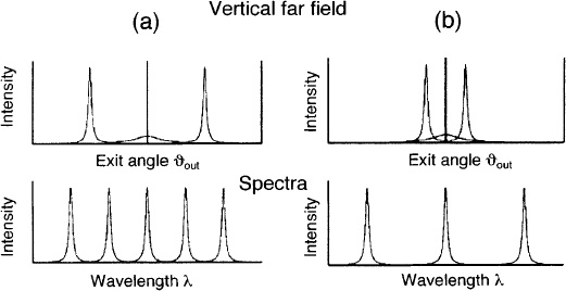
Figure 29. Vertical far field patterns and mode structure in the TCL with substrate reflection. Larger (a) and smaller (b) tilt angles are illustrated.
5. Novel functionality
Epitaxial nanophotonics offers a unique advantage of adding novel functionality to optoelectronic devices. Quantum size effects dramatically modify the optical properties of various optoelectronic media, e.g. enhancing the electrooptic effect by many orders of magnitude. Optical confinement and interference effects in multilayer structures also result in a strong modification of optical properties. When combined, these approaches result in qualitatively new opportunities. For example, by using an electrooptically-modulated (EOM) filter section it becomes possible to achieve ultrahigh-speed intensity modulation in VCSELs.39 The EOM device utilizes resonant interaction between two cavities and can be realized in a surface-emitting geometry or as an edge emitter. The device contains a refractiveindex-tunable element controlled by an applied voltage. Electrooptic modulation is achieved by using the quantum-confined Stark effect in narrow quantum wells and the related modulation of the refractive index. In this scenario, the electrooptic effect is quadratic, because the refractive index change is proportional to the square of the applied electric field, while being inversely proportional to the energy separation between the photon energy and the resonant absorber energy. A schematic illustration of the operating principle, wherein the modulation is realized by the tuning of the resonant wavelength of the “filter” cavity, is shown in Fig. 30.
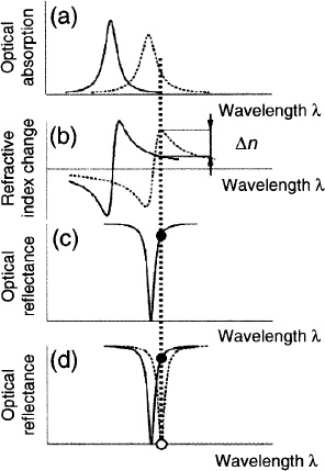
Fig. 30. Electrooptic effect in a vertical cavity. Application of reverse bias (a, b) causes the cavity mode to match the lasing wavelength (c, d) increasing the light output.
Once the refractive index is tuned, the cavity mode of the EOM filter cavity can be shifted towards the resonance with the VCSEL cavity – see Fig. 30(d). The efficiency of light extraction is increased in this case. If the quality factor of the filtering cavity is low enough, no splitting of the cavity modes occurs and only the field intensity at the exit is modulated.
The device contains three electrical contacts to apply laser drive current and reverse modulator bias, as shown schematically in Fig. 31(a). When the bias is applied to the modulator section, the wavelength of the filter section mode is tuned to match the VCSEL cavity mode.
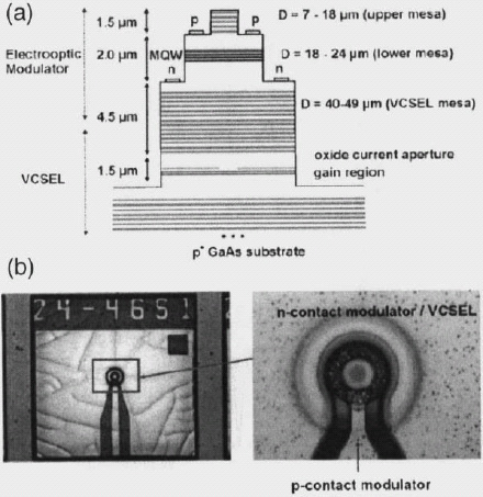
Figure 31. Schematic design (a) and optical microscope image (b) of the EOM VCSEL device.
The EOM VCSEL heterostructure was grown by MBE on a GaAs(100) p- doped substrate.39 The p- and n-doped distributed Bragg reflectors were composed of Al0.9Ga0.1As and GaAs layers. The VCSEL and the modulator cavity were designed to operate at ~960 nm with a blue shift of the modulator cavity by ~3–4 nm. The detuning of the cavities was measured by optical reflectance and photoreflectance spectroscopy and varied across the wafer. Strain-compensated multiple quantum wells (MQWs) were used to provide VCSEL gain at ~960 nm. Straincompensated MQWs with a strong absorption peak at ~930 nm were introduced in the modulator section. Due to growth nonuniformity, the detuning between the cavities varied from 2 to ~10 nm, but this detuning could be compensated by applying a reverse bias in the 2–20 V range.
The sizes of the modulator and VCSEL mesas were chosen to be compatible with >40 Gb/s modulation frequency. BCB planarization was employed for low capacitance contact pads. Wet thermal oxidation of the VCSEL aperture was performed at 400 °C. Optical microscope images of the device are shown in Fig. 31(b).

Figure 32. Static performance of an EOM/VCSEL at different reverse biases applied to the modulator section.
The static performance of on-wafer devices was evaluated by measuring lightcurrent L–I curves at different modulation bias voltages, as well the emission spectra. Device characteristics are strongly affected by the detuning of the two resonant cavities. Figure 32 shows a typical static modulation performance of an EOM VCSEL device in the case of small detuning between the VCSEL and the modulator cavity. At zero bias, the L-I dependence shows a strong resonant feature. This effect originates from thermal shifting of the QW exciton absorption peak in the modulator section with cw current, and the related tuning of the modulator cavity mode. When the reverse bias is applied to the modulator section, there is an additional contribution of the refractive index modulation due to the EOM effect, which shifts the resonance feature towards smaller currents. Thus, we were able to achieve a 2.6 dB/V intensity modulation at very small bias voltages. The devices having a larger detuning between the cavities did not demonstrate such a feature and the application of reverse bias resulted in a modulation of the effective differential efficiency.39
To assess the high speed performance of the devices, optical modulation studies and S21 impedance measurements were performed under different bias voltages. Devices of similar geometry exhibited remarkably consistent characteristics. The estimated electrical modulation bandwidth improved as the modulator mesa siz decreased, from ~33 GHz for 24 μm mesas to ~59 GHz for 18 μm mesas, scaling with the modulator surface area – see Fig. 33.
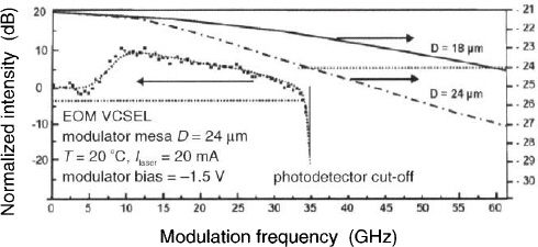
Figure 33. Optical and electrical modulation performance of the EOM/VCSEL, showing the dependence of electrical bandwidth on the modulator mesa diameter D. The speed scales with the surface of the modulator mesa, which defines the capacitance. The maximum optical bandwidth is system limited at 35 GHz.
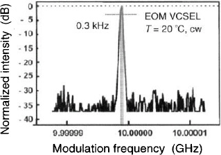
Figure 34. Optical response of the EOM VCSEL under 10 GHz electrical modulation.
Our results thus demonstrate the high-speed potential of these devices and confirms the compatibility of the fabrication technology with > 40 Gb/s modulation regime. We note that the performance is still capacitance-limited even at ~60 GHz. As the active part of the modulator interacting with the oxide-confined VCSEL mode(s) can be restricted down to a few μm, moderate modification of the processing, such as ion implantation into the passive modulator regions, can easily enhance the bandwidth to ~200 GHz or even more. The optical modulation performance of these devices was studied in the 0–40 GHz frequency range. For this on-wafer test, the electrical modulation signal was coupled to the device through a high-frequency contact head. Single mode pin diodes having a low sensitivity in the 960–980 nm range were used due to the lack of high-speed multimode 980 nm photodetectors. As shown in Fig. 33, the modulation bandwidth exceeded 35 GHz and was limited by the cut-off frequency of the photodetector.
Figure 35. Intensity and spectral changes in the single mode EOM VCSEL device.
In Fig. 34 we show an optical response of the detector system when the EOM VCSEL device is operated at 10 GHz. A ~35 dB suppression of parasitic frequencies and a quasi-ideal (<1 kHz) width of the optical response signal is observed. Finally, in Fig. 35 we show spectral evolution in a single mode EOM VCSEL with an oxide aperture size of ~1 μm, where a reverse voltage of 20 V was applied to the modulator section. The intensity is modulated by applying additional bias voltages, as indicated in Fig. 35. A side-mode suppression ratio of >35 dB is obtained. The modulation voltage efficiency factor is up to ~7–10 dB/V. In the vicinity of the resonant modulator voltage, the wavelength chirp is ~0.1 nm/V. Depending on the system application requirements, the design may be adjusted to meet the related specifications imposed by the application.
6. Conclusions
Epitaxial nanophotonics is presently targeting the mainstream applications in optoelectronics.
![]() Self-organized growth: Quantum dots and quantum wires
Self-organized growth: Quantum dots and quantum wires
To date, the key practical applications of self-organized nanostructures are in InGaN light emitting diodes and lasers, where carrier localization in quantum dots enables degradation robustness and spectral control. Further migration of conventional III-V lasers towards higher powers, higher direct modulation speeds, lower optical nonlinearities and better degradation robustness will necessarily require using of QDs for all spectral ranges. Significant market penetration of epitaxial nanostructures is taking place in (In,Ga,Al)P red lasers used for DVD recorders, grown on corrugated surfaces formed on misoriented substrates. Formation of both natural superlattices and the related corrugated GaInP active regions is observed. Effective lateral confinement can be further enhanced by the alloy phase separation at the facets.
![]() Self-organized growth: Defect blocking
Self-organized growth: Defect blocking
Threading dislocations produce significant strain, which can be used to mark the related regions in the vicinity of the dislocation termination at the epitaxial surface. This strain may give rise to numerous effects, such as decoration of the dislocation (in case of the alloy layer growth) or its interaction with self-organized nanoislands. Strain-related effects enable selective capping of the dislocationrelated areas, with subsequent etching of trenches and strain-driven overgrowth. Depending on the type of the dislocation, either complete removal or tilting of the dislocation may be engineered in a controllable way. This enables heterogeneous material integration. The first ever robust high-power lasers on metamorphic substrates28,29 were recently demonstrated using defect reduction. Given sufficient industrial R&D, it may become possible to grown defect-free III-V or SiGe layers on Si or Ge substrates. The III-V integration with Si is of interest in silicon technology to reduce the heat dissipation in high-speed processors. The need in material integration to realize high-efficiency multi-junction solar cells may be another driving force to further develop the DR technology.
![]() Epitaxial nanophotonics
Epitaxial nanophotonics
Novel all-epitaxial approaches promise wavelength-stabilized high-power lasers and the devices with ultranarrow beam divergence. Furthermore, ultanarrow beam operation may be combined with complete wavelength stabilization by using the simplest epitaxial design of back-reflection from transparent substrates. At an advanced stage, light mode velocity engineering, optical nonlinearity, optical bistability and other effects may be engineered.
![]() Novel functionality
Novel functionality
Epitaxial nanophotonics extends the opportunities towards novel functionality. Coupling of the laser cavity to electrooptically-tunable elements may provide ultrahigh-speed wavelength or intensity modulation. An even stronger effect may be realized when electrooptic tuning of the stopband edge of the multilayer interference reflector is applied. The immediate goal of these concepts is to increase dramatically the operating bandwidth and realize cost-effective on-chip arrays of wavelength-tunable devices. Dramatic increase in data traffic (presently at ~250-fold per decade) and the need to comply with ever accelerating productivity of modern computers demands rapid development of ultrahigh-speed low-cost data links. It is widely believed that at speeds beyond 20 Gb/s VCSEL-based optical interconnects will replace conventional copper links.
Acknowledgments
We appreciate collaboration with G. Fiol, F. Hopfer, T. Kettler, M. Kuntz, A. Mutig, and K. Posilovic (Technische Universität Berlin, Institut für Festkörperphysik, Berlin, Germany), Zh. I. Alferov, N. Yu. Gordeev, L. Ya. Karachinsky, M. B. Lifshits, M. V. Maximov, I. I. Novikov, M. Yu. Shernyakov, A. E. Zhukov, and V. M. Ustinov (A. F. Ioffe Physical-Technical Institute, St. Petersburg, Russia), P. Werner and N. Zakharov (Max-Planck Institute for Microstructure Physics, Halle, Germany), H. Krimse and W. Neumann (Humboldt-Universität Berlin, Institut für Physik, Berlin, Germany), A. R. Kovsh (NL-Nanosemiconductor, Germany), N. Grote, H. J. Hensel, H. Klein, W. D. Molzow, and A. Paraskevopoulos (Fraunhofer-Institute for Telecommunications Heinrich-Hertz-Institut, Berlin, Germany). Continuous support from BMBF, DFG, DLR (Germany) and the Russian Foundation for Basic Research is gratefully acknowledged. N.N.L. is a Mercator Professor (DFG).
References
- V. A. Shchukin, N. N. Ledentsov, and D. Bimberg, Epitaxy of Nanostructures, Berlin: Springer, 2003.
- D. Bimberg, M. Grundmann, and N. N. Ledentsov, Quantum Dot Heterostructures, Chichester, UK: Wiley, 1999.
- N. N. Ledentsov, V. M. Ustinov, A. Yu. Egorov, A. E. Zhukov, M. V. Maximov, I. G. Tabatadze, and P. S. Kop’ev, “Optical properties of heterostructures with InGaAs-GaAs quantum clusters,” Semicond. 28, 832 (1994).
- V. A. Shchukin, A. I. Borovkov, N. N. Ledentsov, and D. Bimberg, “Tuning and breakdown of faceting under externally applied stress,” Phys. Rev. B 51, 10104 (1995).
- R. Nötzel, N. N. Ledentsov, L. Däweritz, K. Ploog, and M. Hohenstein, “Semiconductor quantum wire structures directly grown on high-index surfaces,” Phys. Rev. B 45, 3507 (1992).
- R. Noetzel, N. N. Ledentsov, L. Daeweritz, and K. Ploog, “Method of fabricating a compositional semiconductor device,” U.S. Patent 5, 714, 765 (1998).
- S. Nakamura, M. Senoh, S. Nagahama, et al., “Subband emissions of InGaN multi-quantum-well laser diodes under room-temperature continuous wave operation,” Appl. Phys. Lett. 70, 2753 (1997).
- N. N. Ledentsov “Vertical-cavity surface-emitting lasers using InGaN quantum dots,” Compound Semicond. 5, 61 (1999).
- R. Seguin, S. Rodt, A. Strittmatter, et al., “Multi-excitonic complexes in single InGaN quantum dots,” Appl. Phys. Lett. 84, 2753 (2004).
- I. L. Krestnikov, N. N. Ledentsov, A. Hoffmann, et al., “Quantum dot origin of luminescence in InGaN-GaN structures,” Phys. Rev. B 66, 155310 (2002).
- I. Krestnikov, D. Livshits, S. Mikhrin, A. Kozhukhov, A. Kovsh, N. N. Ledentsov, and A. Zhukov, “Reliability study of InAs-InGaAs quantum dot diode lasers,” Electronics Lett. 41, 1330 (2005).
- N. N. Ledentsov, A. R. Kovsh, V. A. Shchukin, et al., “1.3–1.5 μm quantum dot lasers on foreign substrates: Growth using defect reduction technique, high-power cw operation, and degradation resistance,” Proc. SPIE 6133, 61330S (2006).
- F. Hopfer, A. Mutig, G. Fiol, et al., “20-Gb/s direct modulation of 980 nm VCSELs based on submonolayer deposition of quantum dots” Proc. SPIE 6350, 6 (2006).
- N. N. Ledentsov and V. Shchukin, “Optoelectronic device based on an antiwaveguiding cavity,” U.S. Patent application 2005/0226294, published October 13, 2005.
- L. Goldstein, F. Glas, J. Y. Marzin, M. N. Charasse, and G. Leroux, “Growth by molecular-beam epitaxy and characterization of InAs/GaAs strained-layer superlattices,” Appl. Phys. Lett. 47, 1099 (1985).
- F. Glas, C. Guille, P. Hénoc, and F. Houzay “TEM study of the molecular beam epitaxy island growth of InAs on GaAs” in: A. G. Cullis and P. D. Augustus, eds., Proc. Microscopy Semiconducting Mater. (1987), Oxford: Institute of Physics, 1987.
- O. Brandt, M. Ilg, and K. Ploog, “Coherently strained InAs insertions in GaAs: Do they form quantum wires and dots?” Microelectronics J. 26, 861 (1995).
- N. N. Ledentsov, M. Grundmann, N. Kirstaedter, et al., “Ordered arrays of quantum dots: Formation, electronic spectra, relaxation phenomena, lasing,” Solid State Electronics 40, 785 (1996).
- N. N. Ledentsov, V. A. Shchukin, D. Bimberg, et al., “Reversibility of the island shape, volume, and density in Stranski-Krastanow growth,” Semicond. Sci. Technol. 16, 502 (2001).
- N. N. Ledentsov, M. V. Maximov, D. Bimberg, et al., “1.3 μm luminescence and gain from defect-free InGaAs-GaAs quantum dots grown by metalorganic chemical vapour deposition.” Semicond. Sci. Technol. 15, 604 (2000).
- D. S. Sizov, M. V. Maksimov, A. F. Tsatsul’nikov, et al., “The influence of heat treatment conditions on the evaporation of defect regions in structures with InGaAs quantum dots in the GaAs matrix,” Semicond. 36, 1020 (2002).
- N. N. Ledentsov, “Semiconductor device and method of making same,” U.S. Patent 6,653,166 (2003).
- V. A. Shchukin and N. N. Ledentsov, “Defect-free semiconductor templates for epitaxial growth and method of making same,” U.S. Patent 6,784,074 (2004).
- N. N. Ledentsov and D. Bimberg, “Growth of self-organized quantum dots for optoelectronic applications: Nanostructures, nanoepitaxy, defect engineering,” J. Cryst. Growth 255. 68 (2003).
- N. N. Ledentsov, A. R. Kovsh, V. A. Shchukin, et al., “QD lasers: Physics and applications,” Proc. SPIE 5624, 335 (2005).
- A. Lenz, H. Eisele, R. Timm, et al., “Nanovoids in InGaAs/GaAs quantum dots observed by cross-sectional scanning tunneling microscopy,” Appl. Phys. Lett. 85, 3848 (2004).
- N. N. Ledentsov, A. R. Kovsh, A. E. Zhukov, et al., “High performance quantum dot lasers on GaAs substrates operating in 1.5 μm range,” Electronics Lett. 39, 1126 (2003).
- T. Kettler, L. Ya. Karachinsky, N. N. Ledentsov, et al., “Degradation-robust single mode continuous wave operation of 1.46 μm metamorphic quantum dot lasers on GaAs substrate,” Appl. Phys. Lett. 89, 041113 (2006).
- L. Ya. Karachinsky, T. Kettler, N. Yu. Gordeev, et al., “High-power single mode cw operation of 1.5 μm-range quantum dot GaAs-based laser,” Electronics Lett. 41, 478 (2005).
- N. N.Ledentsov and V. A. Shchukin, “Novel concepts for injection lasers,” SPIE Optical Eng. 41, 3193 (2002).
- V. A. Shchukin and N. N. Ledentsov, “Semiconductor laser based on the effect of photonic band gap crystal-mediated filtration of higher modes of laser radiation and method of making same,” U.S. Patent 6,804,280 B2 (2004).
- M. V.Maximov, Yu. M. Shernyakov, I. I. Novikov, et al., “High power GaInP/AlGaInP visible lasers (λ = 646 nm) with narrow circular shaped far field pattern,” Electronics Lett. 41, 741 (2005).
- I. I. Novikov, L. Ya. Karachinsky, M. V. Maximov, et al., “Single mode cw operation of 658 nm AlGaInP lasers based on longitudinal photonic band gap crystal,” Appl. Phys. Lett. 88, 231108 (2006).
- V. A. Shchukin, N. N. Ledentsov, N. Yu. Gordeev, et al., “High brilliance photonic band crystal lasers,” Proc. SPIE 6350, 635005 (2006).
- N. N. Ledentsov and V. A. Shchukin, “Tilted cavity semiconductor laser (TCSL) and method of making same,” U.S. Patent 7,031,360 (2006).
- N. N. Ledentsov, V. A. Shchukin, S. S. Mikhrin, et al., “Wavelength-stabilized tilted cavity quantum dot laser,” Semicond. Sci. Technol. 19, 1183 (2004).
- N. N. Ledentsov, V. A. Shchukin, A. R. Kovsh, et al., “Edge and surface-emitting tilted cavity lasers,” Proc. SPIE 5722, 130 (2005).
- N. N. Ledentsov and V. A. Shchukin, to be published.
- A. Paraskevopoulos, H.-J. Hensel, W.-D. Molzow, et al., “Ultra-highbandwidth (>35 GHz) electrooptically-modulated VCSEL,” paper PDP22 presented at OFC/NFOEC 2006, Anaheim, CA (March, 2006).