
Wavelength Tuning of Interband Cascade Lasers Based on the Stark Effect
State University of New York at Stony Brook, Stony Brook, NY 11794-2350, U.S.A.
Maxion Technologies, Inc., Hyattsville, MD 20782-2003, U.S.A.
Army Research Laboratory, Adelphi, MD 20873-1197, U.S.A.
1. Introduction
Tunable mid-IR lasers are in high demand for various military and civilian applications, such as free space communication, remote sensing, and environmental monitoring. The Stark effect, that is the energy level shift in an external electric field, provides an attractive mechanism for semiconductor laser tuning in that it allows an ultrafast and fully electrical control over a broad range of emission wavelengths. This mechanism is especially promising for cascade lasers, both type-I quantum cascade lasers (QCLs) and type-II interband cascade lasers (ICLs), where the spatially indirect lasing transition can be easily tuned with a strong first-order Stark shift. There is one major obstacle, however, on the way to a practical implementation of the Stark-effect tunable device. The laser generation condition (gain equals loss) usually pins the carrier concentration in the laser active region above threshold at a fixed level (the so-called concentration clamping effect). The concentration clamping does not allow any changes of the electric field in optically active layers by pinning the field to its threshold value and, therefore, prevents the Stark shift of the lasing levels.
Threshold clamping can be circumvented by a special laser design. Partitioning the laser structure in multiple sections1 is the most straightforward way to achieve above-threshold laser tuning. In this approach, the additional gain/loss from the auxiliary section of the laser waveguide modifies the threshold condition in the main lasing section. The different threshold current implies a different threshold concentration in the active region and, correspondingly, different electric field that results in a Stark shift of the lasing transition. Shortcomings of this approach are also straightforward – multi-sectioned design implies a complicated multi-electrode control of the laser action. As an alternative, a complementary section can be incorporated directly into the laser active region with some control functions that should depend on the total bias current. This approach was first suggested for type-I quantum well (QW) laser diodes.2 The controlling sections were represented by additional accumulation QWs located in the active region on each side of the optically active QW. Such outside carrier accumulation is not restricted in any way by the threshold condition and hence it is capable of unclamping the electric field in the active layers. The tuning of the main lasing transition was, therefore, achieved by the bias injection current alone. The tunability range, however, was quite small because of the weak second-order Stark effect in active QWs.
In this chapter, we apply the concept of outside accumulation to a type-II ICL design, taking full advantage of the strong first-order Stark effect in a cascade structure. We show that this approach allows efficient all-electrical control of the peak gain position and demonstrate high-speed tuning of the laser wavelength.
2. The tuning concept
Type-II ICL is especially promising for electrical tuning due to the inherently strong first-order Stark effect in interband cascade structures. Indeed, in a type II structure, the recombining electrons and holes are spatially separated, so that there is a nonzero dipole moment in the growth direction even in the absence of an applied field. The key element of our approach is a specially designed tunnel barrier that separates injected electrons into two groups. One group of electrons is directly involved in the optical transition between electron and hole states of the optically active region, which in our design includes an asymmetric type-II heterojunction or a type-II double-QW heterostructure – see Fig. 1, layers 1 and 2. The other group of the injected electrons is accumulated in a specially provided QW (layer 3) located outside the optically active layers. The tunnel barrier 4 separates the accumulation QW from optically active layers. The electric charge accumulated in the accumulation QW provides an additional electric field that modifies the electron energy spectrum in the optically active layers 1 and 2 through the linear Stark effect.
As the injection current increases above threshold, the density of electrons in the accumulation QW grows in proportion to the current. Simultaneously, holes accumulate in the hole QW (layer 1). This charge separation results in an electric field increasing with the injection current after the laser threshold. The energy level positions E2 and E1 (and hence the emission wavelength λ) become dependent on the bias current that controls the electric field via the charge accumulation in the electron accumulation QW (layer 3) and hole QW (layer 1). Separation of the electron charge accumulation layer 3 from the optically active layers 1 and 2 enables the wavelength tuning above the laser threshold. At current densities J ≥ JTH, the maximum net modal optical gain is zero:
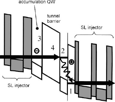
Figure 1. Band diagram of the structure under bias.
Here, n2(c) is the electron concentration in the electron quantum well 2, n1(h) is the hole concentration in the hole quantum well 1, N2D = 2kTme*/π![]() 2 and P2D = kTmh*2/π
2 and P2D = kTmh*2/π![]() 2 are effective 2D densities of states in the conduction and valence subbands, G0 is the saturation gain, and α is the optical loss.3 The concentration in the electron accumulation layer 3 can be estimated in a steady state regime by n3(c) = J
2 are effective 2D densities of states in the conduction and valence subbands, G0 is the saturation gain, and α is the optical loss.3 The concentration in the electron accumulation layer 3 can be estimated in a steady state regime by n3(c) = J![]() tun/q, where
tun/q, where ![]() tun is the tunneling time and q is the electron charge. Using the charge neutrality condition, n1(h) = n3(c) + n2(c), the electron concentration in the active quantum well is related to the injection current density J by the equation:
tun is the tunneling time and q is the electron charge. Using the charge neutrality condition, n1(h) = n3(c) + n2(c), the electron concentration in the active quantum well is related to the injection current density J by the equation:
It is essential to note that while the generation condition (1) clamps the gain, it no longer pins either of the two concentrations n1(h) and n2(c), which remain current-dependent, as seen explicitly from Eq. (2). As the concentration in the electron accumulation layer n3(c) increases with the current, so does the hole concentration n1(h); both the overall charge neutrality and the modal gain pinning are satisfied without preventing the increase of the electric field in the active type-II heterojunction region. The latter, in turn, affects the laser wavelength tuning above threshold.
3. Tunable structure
The tunable ICL structure was grown by MBE on p-doped GaSb substrate. The laser core contained a cascade of 14 periods. Each period included a digitally graded InAs/AlSb injector with accumulation QW and InAs/Ga0.8In0.2Sb type II optically active double quantum well heterostructure, separated from each other by a 4 nm AlSb tunneling barrier. The widths of the InAs and Ga0.8In0.2Sb layers were 2.1 nm and 3.1 nm, respectively. The Ga0.8In0.2Sb layer was followed by p-doped 5.8 nm GaSb QW that served as a hole reservoir. The active area was sandwiched between InAs/AlSb superlattice cladding layers. The devices were fabricated as deep-etched mesas and soldered, epilayer side up, to Au-coated copper mounts. The mesas were 35 μm wide with 0.5-mm-long cavity. Both facets were left uncoated. The mounts were attached to the cold finger of a liquid N2 or Helitran cryostat. The emission was collected with reflection optics and analyzed with an FTIR spectrometer. We compared the tuning characteristics of this structure with those of a regular 18-cascade ICL.4 The latter had an active region with type II W-like quantum wells and contained no special tunnel barriers for charge accumulation.
The current–voltage dependence of the structure is shown in Fig. 2. The experimental turn-on voltage is ~5.2 V and agrees well with the calculated value 4.9 V for an ideal 14-period cascade structure. Calculation shows that a voltage drop of 0.35 V per each injector region provides for injector level alignment. For 56 nm injectors this corresponds to the turn-on internal electric field of ~65 kV/cm.

Figure 2. Current-voltage dependence of the tunable cascade laser.
As the bias current reaches ~650 mA, the voltage jumps from ~8.5 V to ~14.5 V. There is no such a jump in the regular IC laser. This effect indicates switching into another conducting state and is indicative of the negative differential resistance instability associated with the resonant tunneling between layers 3 and 2. The switching may be accompanied by charge build-up in the accumulation quantum well. The switching is reversible and the bias current can be increased further after the voltage jump until the electrical breakdown of the dielectric separating the upper metal contact from the substrate occurs. A possible explanation of this behavior is that at higher bias current the charge accumulation and subsequent voltage drop leads to the energy alignment of the accumulation level and the second subband of the InAs/GaInSb laser quantum well. According to calculations, this subband is ~0.5 eV higher than the upper lasing level. The width of the tunnel barrier 4 in our design was chosen as 4 nm to ensure the alignment of the accumulation level 3 and upper lasing level 2 at turn-on voltage (see Fig. 1). As the charge builds up in the accumulation well, this alignment breaks due to the voltage drop across the barrier. This does not necessarily mean immediate disruption of the carrier injection into the upper lasing level. Effective injection can be maintained within a finite range of the energy mismatch. This range is determined by the width of the injector miniband, formed at turn-on voltage, as well as inelastic tunneling processes.5 As the energy mismatch increases further, the net tunneling rate decreases in spite of the increasing carrier density build-up in the accumulation quantum well. Enforcing the bias current at these conditions may provide a positive feedback for carrier accumulation and, as a result, uncontrollable increase of the voltage drop until higher energy states in the type II quantum well are aligned with the accumulation level. Assuming that these states belong to the second subband in the InAs/GaInSb double quantum well, we can estimate the total voltage jump as ~7 V for a 14 cascade structure. This agrees well with the observed voltage jump of ~6V.
4. Optical characteristics
The electroluminescence (EL) spectrum at low current is shown in the inset of Fig. 3. The emission energy quantum of 0.34 eV agrees with the calculated value of 0.32 eV. The EL spectral maximum energy increases linearly with the bias voltage. Since this dependence was measured in the subthreshold pumping region, the linear shift should be attributed to the Stark effect that results from charge accumulation in the type II quantum wells of the laser active area. A similar effect has been observed in a regular interband cascade laser (see Fig. 3), though there the effect was weaker due to the smaller electron-hole dipole in active W-quantum wells.
The optical gain spectra measured with the Hakki-Paoli technique are shown in Fig. 4. The modulation of the gain spectra is a manifestation of “leaky” modes.6 This effect also manifests itself in the modulation of the amplified spontaneous emission (ASE) spectra and mode grouping in the lasing spectra. The observed threshold current density is 91 A/cm2 at 80 K. The lasers demonstrate cw operation up to 120 K and pulsed operation up to 200 K (pulse duration = 400 ns, duty cycle = 2.4%). The external quantum efficiency is ~250% (at 80 K). The internal loss is ~10 cm-1 (Fig. 4).

Figure 3. Dependence of the electroluminescence (EL) energy quantum on the bias voltage for a regular IC laser (triangles) and tunable IC laser (circles). Inset shows the EL spectrum at low bias current.
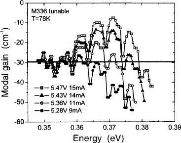
Figure 4. Modal gain spectra of the tunable laser at different bias currents.
5. Laser tunability
Amplified spontaneous emission and lasing spectra of both the tunable and the regular IC lasers are shown in Figure 5. In the regular laser, in spite of the ASE blue shift, the laser line spectral position is stable up to high bias currents (~220 times JTH). This is as expected from the pinning of concentration and, hence, of electric field in the active area quantum wells.
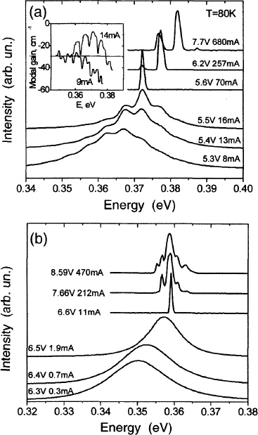
Figure 5. ASE and laser spectra of the tunable IC laser (a) and regular IC laser (b) at different bias currents. The inset in the panel (a) shows the modal gain spectrum of the tunable IC laser.
The lasing spectrum of the tunable laser (see Fig. 5(a), three upper curves) clearly demonstrates a blue shift. The periodic modulation of the ASE spectrum in the tunable laser is consistent with the observed strong modulation of the modal gain spectrum with the same period (see Fig. 4 and Fig. 5(a), inset). The spectral positions of the gain modulation maxima and minima are determined by the substrate thickness, as well as by the effective refractive indices of the active area, cladding layers, and substrate. The dependence of the modulation peak positions on the bias current is weaker than the Stark shift of the gain spectrum. As the bias current increases, the material gain curve shifts with respect to the modulation extremes and consequently, the modal gain maximum shows a discrete blue shift with the increments equal to the leaky mode modulation period. This behavior takes place at pumping levels far above the laser threshold. The lasing spectrum of the tunable laser demonstrates a blue shift with increasing bias current. The rate of thiq shift with respect to the bias current (and voltage) is slower than the rate of ASE tuning in the subthreshold region (approximately 5 meV/V vs. 30 meV/V). This indicates an abrupt change in the tuning mechanism as the bias current exceeds the laser threshold. In the subthreshold regime, the wavelength shift is determined primarily by the carrier accumulation in the optically active quantum wells and is related to the corresponding increase of the internal electric field in the type–II heterojunction.
After the laser threshold has been reached, the wavelength tuning becomes determined by the charge buildup in accumulation quantum well 3, which, in turn, depends on the electron tunneling rate through the barrier 4. Figure 6 demonstrates the laser spectrum shift recorded throughout the whole range of the injection current (1–42 threshold values) without noticeable saturation. The maximum value of the laser emission tuning range is 15 meV or 120 nm.

Figure 6. Lasing spectra of the tunable IC laser vs. injection current.
6. Modulation response characteristics
One of the principal advantages of the presented tuning scheme in comparison with temperature tuning is the possibility of fast wavelength modulation. To show the potential of the Stark tuning for high-speed applications, we measured the frequency response of the laser tuning. To do this, we combined the above-threshold dc bias component with ac bias component. The frequency of the ac component was varied in the range 0.01–2 GHz. While the bias modulation period is larger than the tuning response time of the laser, the laser spectrum shape is changing simultaneously with the bias. Since the spectrometer response time is larger than the bias modulation period over the whole modulation frequency range, the measured spectrum is the result of time averaging over all spectral shapes corresponding to the bias values within the modulation amplitude. As the bias modulation period becomes smaller than the laser tuning response time, the laser wavelength is not affected anymore by the bias modulation and the measured spectrum corresponds to dc component of the bias. By monitoring the change of the laser spectrum shape with the bias modulation frequency, we can estimate the tuning modulation bandwidth.
For the measurements of the frequency dependence of the wavelength tuning we used the 0.5 mm long laser with the mesa width of 8 μm and threshold current of 6 mA at 80 K. The differential resistance of the laser at the given dc bias is 6.9 Ω. A high frequency 47 Ω resistor was connected in series with the laser for the cable impedance matching. The dc bias current was 31 mA; the ac modulation amplitude was ~25 mA. For the 31 mA bias, the laser spectrum consists of a single line (further referred to as line 1). As the bias current increases to ~40 mA, another line (line 2) corresponding to the next “leaky mode maximum” appears due to the gain curve shift. The presence of line 2 in the time-averaged spectrum means that the tuning response time is shorter that the laser modulation period. At higher frequencies line 2 disappears and the spectrum returns to that without modulation (Fig. 7). The relative amplitude of the second line as a fbnction of frequency in Fig. 7 provides a rough estimation for the modulation bandwidth. The sharp decrease of the line 2 intensity takes place at ~1.6 GHz. The vanishing of the line 2 means that the peak bias current decreased from 56 mA to ~40 mA so the modulation amplitude decreased by a factor of ~2.5.
The bandwidth for the Stark wavelength modulation can be estimated as v ~(2πRC)-1, where C is the capacitance of the device and R is the series resistance of the laser. The capacitance is the sum of the parasitic capacitance of the laser package CP and internal capacitance of the laser structure CL. To estimate CL we consider the active areas in each period as plate capacitors connected in series by the conducting injectors. The electron and hole accumulation quantum wells represent the capacitor plates. The 8 × 500 μm plates are separated by the distance of ~80 Å. Taking the relative dielectric constant ε ~ 12, we obtain CL ~ 4 pF for the 14 cascade laser. At the series resistance of R ~ 6.9 Ω, the tuning bandwidth is ~6 GHz. In our case the cutoff is most probably determined by CP, which is ~20 pF. This corresponds to the bandwidth of ~1.2 GHz, in a good agreement with the experimental results.

Figure 7. Lasing spectra at different modulation frequencies (a); frequency dependence of the intensity of line 2 (b).
7. Conclusions
The concept of outside carrier accumulation has been applied to a type-II ICL design to take full advantage of the strong first-order Stark effect in a cascade structure. Our design of the Stark-effect tunable ICL includes an additional electron accumulation layer located outside the optically active type-II quantum well heterostructure. This eliminates the pinning of the electron-hole concentration to the threshold value and enables ultra-wide Stark shift of the optical gain spectrum. We experimentally demonstrate an electrically tunable ICL operating in the mid-IR spectral range with tuning range of 120 nm (starting from the initial lasing wavelength ⌊ ~ 3.33 ⌠m), or 120 cm-1. We also demonstrate wavelength modulation at frequencies up to 1.6 GHz. The ICL tuning performance can be further improved by suppressing the gain spectrum modulation due to the substrate leaky modes.
Acknowledgements
This work was supported by ARO grant DAAD 190310259.
References
- J. Faist, F. Capasso, C. Sirtori, D. L. Sivco, A. L. Hutchinson, and A. Y. Cho, “Laser action by tuning the oscillator strength,” Nature 387, 782 (1997).
- N. Le Thomas, N. T. Pelekanos, Z. Hatzopoulos, E. Aperathitis, and R. Hamelin, “Tunable diode lasers by Stark effect”, Appl. Phys. Lett. 83, 1304 (2003).
- V. B. Gorfinkel and S. Luryi, “Fundamental limits of linearity for CATV lasers”, J. Lightwave Technol. 13, 252 (1995).
- J. L. Bradshaw, N. P. Breznay, J. D. Bruno, et al., “Recent progress in the development of type II interband cascade lasers”, Physica E 20, 479 (2004).
- M. V. Kisin, S. Suchalkin, and G. Belenky, “Stark effect tunable QCL”, 8th Intern. Conf. Intersubband Transitions Quantum Wells ITQW-2005, North Falmouth, MA (September, 2006).
- D. Westerfeld, S. Suchalkin, M. V. Kisin, G. Belenky, J. Bruno, and R. Tober, “Experimental study of optical gain and loss in 3.4–3.6 μm interband cascade lasers”, IEE Proc. Optoelectron. 150, 293 (2003).