
Will the Insulated Gate Transistor Concept Survive Next Decade?
Dept. of Microtechnology and Nanoscience
Chalmers University of Technology, SE-412 96 Göteborg, Sweden
1. Introduction
The increasing influence of electronics on human life in the past couple of decades has promoted the MOS transistor to a device of similar significance for cultural change as, for example, the rotating electric motor and the combustion engine. A key property of the MOSFET, which has made this ranking possible, is its potential for fast and steady improvement. In the early 1970’s, when the current-voltage characteristics of the device reasonably well could be described by the one-dimensional Ihantola-Moll model,1 the gate channel was long enough that the electrostatic influence from source and drain contacts could be neglected or considered as a slight perturbation at higher drain voltages. The downscaling process, which has been going on since then, is presently at a stage where the electric field distribution between source and drain has become too complicated for simple analytical expressions in characterizing the device. Bulk CMOS technology has reached a point where further development includes a considerable “squeezing” of parameter values by small geometrical changes and by the introduction of novel materials, combined with the acceptance of numerous tradeoffs in the design process.
Many of these problems in the scaling of bulk MOSFETs have a straight-forward solution in silicon-on-insulator (SOI) technology. Especially when using fully depleted materials, double-gate or fin-FET devices are very attractive for solving the electric field problems mentioned above due to their excellent control of the field distribution in the channel.
For bulk CMOS devices, solutions seem to exist to satisfy the requirements of the 45 nm node, with physical gate lengths between 18 and 25 nm depending on the application.2 Beyond this milestone, however, common wisdom among specialists points in the direction of SOI technology for use in the 32 and 22 nm nodes, which are planned to be developed by 2013 and 2016, respectively.3,4 The title of this chapter, therefore, could be reformulated more specifically: “Will it be possible within a decade to reach the 22 nm node with currently used MOSFET concepts?” A couple of the most important problems in this context will be discussed below.
2. The downscaling problem of bulk CMOS
For the classical MOS transistor, the channel region meets the source and drain via the depletion regions occurring between the two different doping types constituting the three building blocks of source, drain and bulk, as shown in Fig 1. As long as the gate length is much larger than the depleted distances, the influence of the field distribution from source and drain on the threshold voltage is negligible. This makes the electric vector field from the gate point perpendicular to the channel. However, when decreasing the gate length of bulk CMOS transistors, a pronounced mixing with the fields from source and drain complicates the field distribution under the gate and lowers the threshold voltage. Also, current leakage may occur between source and drain due to the shrinking distance between the depletion edges surrounding the two contacts. This has been a recurring problem, labelled the “short channel effect”, during the entire history of MOSFET downscaling.5 For bulk CMOS technology, it has forced designers to invent new geometries for the doping profiles of the source and drain. Also, in order to decrease the source and drain depletion regions, the doping concentration under the gate has been continuously increased in the process of shortening the gate. This move, however, lowers the capacitive coupling between gate and channel, which is detrimental for the switching behaviour of the transistor.
When the transistor is switched on and off by changing the gate voltage, it is desirable that as much as possible of the voltage change be transferred to the semiconductor. This means that the capacitance of the gate insulator must be large compared to the series-connected capacitance of the semiconductor region under the gate. The gate capacitance can be increased by decreasing the thickness of the gate insulator. With present SiO2 and SiON dielectrics such adjustments are approaching the limits set by unacceptable gate leakage due to tunneling. This has motivated a chase for novel dielectric materials with high dielectric constants (“high-κ”), able to maintain the capacitive coupling for thicker insulator layers and thus decrease tunneling currents.6 The numerical calculations for MOS capacitors in Fig. 2 correlate the gate voltage and oxide voltage for different doping concentrations and κ-values, respectively. For a channel doping concentration between 1018 and l019 cm-3, which will be required for a possible bulk CMOS technology at the 22 nm node, it is seen that a κ-value higher than 15 is needed for an insulator thickness of 20 Å. The effective bending of the energy bands in the semiconductor for a given change in gate voltage is necessary in order to obtain a reasonable value of the “subthreshold swing”. This is the change in gate voltage needed to reduce the drain current by one order of magnitude, which is an important parameter determining the on/off behaviour of the transistor.
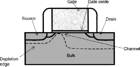
Figure 1. Schematic cross-section of a bulk MOSFET. The dashed curve schematically indicates the depletion edge for a high drain voltage.
From this reasoning, the scaling problem for bulk CMOS can be described as a balance between high doping levels and gate capacitive coupling. In order to improve the field distribution under the gate, higher doping is necessary. which leads to a need for increased gate coupling. This in turn requires a thinner gate insulator, which eliminates SiO2, used so far in MOSFET history, as a dielectric material because of unacceptable gate leakage current.7
Another possibility for improving the electric field distribution would be to create a doping distribution under the gate, a “super-halo”, that would compensate for the influence from the source and drain depletion regions.8 Such distributions have been suggested by simulation studies and seem possible to obtain by using advanced ion implantation techniques. However, the complexity of such a solution must be compared to a possible changeover to SOI technology, as described below. In both cases, a high-κ gate dielectric will probably be necessary in order to reach the 22 nm node.
In the historical process of improving the field distribution under the gate to avoid short channel effects, the depths of source and drain diffusions have been decreased. This gives rise to an increasing series resistance and encroaches on the achievable values of the on-current and switching capability. In recent years, novel source/drain solutions have been investigated by using Schottky contacts instead of the traditional pn junctions.9 Increased series resistance is not only a problem for bulk CMOS; it appears similarly in SOI technology.
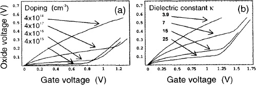
Figure 2. Voltage across the oxide as a function of gate voltage for an MOS structure vs. varying semiconductor doping concentrations (a) and vs. dielectric constant κ of the gate insulator (b).
3. High-κ dielectrics and bulk CMOS technology
From the processing point of view, one of the most important advantages of silicon technology has been the existence of silicon dioxide, used as a masking and insulating material in the production of integrated circuits. This is especially true for the use of this material as a gate insulator of MOSFETs. The requirements on a replacement material, therefore, are very stringent. Not only the physical properties – interface and bulk charges, scattering of charge carriers in the channel, and energy band offsets compared to silicon – but also the chemistry that provides thermal stability during the processing sequence must be controlled with high precision. The fundamental current leakage is determined by tunneling that, in turn, depends on the thickness and the band offset barriers for electrons and holes between the conduction and valence bands of the silicon and the dielectric. Consequently, if the dielectric constant of the material is not high enough to allow for a small enough thickness in combination with high enough offset values, a chosen material cannot be used even if all other properties are promising.
In order to compare the thickness requirement of different gate dielectrics, the concept of “equivalent oxide thickness” (EOT) is used. This quantity expresses the thickness of silicon dioxide, with dielectric constant κSiO2, that is needed to give the same capacitance as an alternative high-κ insulator with a dielectric constant κH and thickness tH: EOT = tH(κSiO2/κH). For the 22 nm node and low standby power (LSTP) technology, the ITRS roadmap forecasts a physical gate length LG = 13 nm and an EOT of 5–6 Å for the gate insulator of bulk CMOS devices.10 The problem of finding a suitable high-κ material has inspired much research and development activity at laboratories around the world.6,7
The gate leakage current requirement given by the ITRS roadmap10 is expressed in terms of current per gate length. For a transistor, gate leakage includes leakage not only to the channel, but also to the source and drain due to gate overlap. Corresponding values expressed as a current density have been estimated and for LSTP in the 22 nm node, a leakage current of 10−2 A/cm2 has been considered as reasonable.11 Using this value and EOT = 0.5 nm as stated above, it is possible to calculate a limit line for the combination of dielectric constant κH and offset value ΔEC that will meet the gate leakage requirement. In a recent paper this was done for different oxides, considered as candidates for future CMOS dielectrics, in the κH and ΔEC parameter space.12 The starting point of this investigation was the finding that La2O3 fulfils the requirements mentioned above.13 Using this material as a reference, the limit line for the 22 nm node was estimated for direct and Fowler-Nordheim tunneling under the EOT = 0.5 nm condition and the result is depicted in Fig. 3. From this graph, only a few dielectrics are of interest for 22 nm LSTP devices. The data in Fig. 3 only take into account the conduction band energy offset values ΔEC. From the bandgap values of the different oxides and of silicon, the corresponding offset values for the valence bands were also estimated. This left only La2O3 and LaAlO3 as clearly interesting dielectrics from the fundamental requirement of tunneling current leakage. Taking into consideration that the estimates giving rise to the limit lines in Fig. 3 are relatively rough and that available experimental data may suffer from varying inaccuracies, some other materials like Pr2O3 and Gd2O3 close to the boundaries may serve as additional candidates. Even so, it should be emphasized that Fig. 3 only represents the basic condition of tunneling leakage. Other properties, like reduced mobility due to carrier scattering at the oxide-silicon interface, oxide bulk charges influencing threshold voltage variations, and thermal stability6,7 are obstacles on the road to technically acceptable high-κ oxides.

Figure 3. Offset barrier heights between conduction bands for different oxides and silicon plotted as a function of dielectric constant κH. The two curves represent estimated borders for the ITRS low stand-by power (LSTP) requirements at the 22 nm node: solid curve is for Fowler-Nordheim tunneling, dashed curve for direct tunneling. Dots represent experimental data (ΔEC) taken from literature; triangles are data from empirical relations (ΔECH) for physical trends (from Ref. 12).
4. Fully-depleted multiple-gate SOI technology
Silicon-on-insulator technology inherently improves the complicated electric field distribution under the gate.3 Transistors fabricated by using SOI as a starting material are made in a thin silicon film on top of a silicon dioxide layer that, in turn, rests on a silicon wafer.14 This allows for a better field control, especially for a “fully depleted” geometry in which the silicon layer thin enough that the depletion region from the gate reaches the buried oxide on the wafer underneath. Also, a number of ideas have been put forward for increasing the gate control by using multiple gate structures, including double-gate, triple-gate and “gate-all-around” geometries, where the names correspond to the number of directions from which a gate is applied to a thin slice of Si or a Si wire.15 Controlling the channel electric field in a thin slice or wire from opposite planes held at the same potential, drives the potential along the channel extension towards a constant value. From a fabrication point of view, the double-gate structure seems to be the most likely to enter production over the next decade, especially when designed as a standing slice to build the so-called fin-FET illustrated in Fig. 4.15 This is believed by many to be the least complicated method to make a fully-depleted double-gate MOS transistor on SOI (FD-DGSOI) and appears as the most promising candidate for future production if bulk CMOS reaches its limits.4
Even if the thin silicon layer between the two gates of a FD-DGSOI transistor provides better electric field control along to the channel, a competition with the lateral fields from the depletion regions of source and drain exists also in this structure.16 This originates from the relations between, on the one hand, oxide properties like dielectric constant κ and thickness tox, and, on the other hand, the thickness of the silicon film, tSi. For a shorter gate length LG, a thinner silicon layer will be needed. A “natural length” λ sets the length scale from which the smallest possible dimensions can be estimated. Expressions for λ values valid for multiple-gate geometries have been derived by a number of authors.15,17 For the central part of a FD-DGSOI intrinsic Si transistor channel at zero gate voltage and zero flatband voltage, the electric potential Φ(x) along the channel coordinate x, is described by:15,17
where

Figure 4. Double gate SOI transistor shaped as a fin-FET.
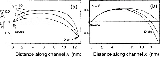
Figure 5. Conduction band variation along the intrinsic channel of a double-gate SOI transistor with LG = 13 nm gate length for a drain voltage of 0.7 V with three different values of γ = LG/λ (a); and for γ = 5 with three different drain voltages VD = 0, 0.4 and 0.7 V (b).
Using the boundary conditions Φ(x=0) = 0, Φ(x=LG) = 0.7 V, we find the standard solution of Eq. (1) as a combination of sinh terms. Further, expressing the silicon conduction band edge EC(x) = −qΦ(x), we find the plot shown in Fig. 5(a). As long as the conduction band edge in this graph has a flat region, one may expect that the change in gate voltage needed to increase the drain current will be close to the ideal value (kBT/q)ln 10 ≈ 60 mV/decade at room temperature. We notice in Fig. 5(a) that this criterion is fulfilled when the ratio γ ≡ LG/λ = 10, but this is no longer the case when γ approaches 3.
A second important property for a short channel MOSFET is “drain-induced barrier lowering” (DIBL), which is the decrease in maximum potential along the channel due to an increased drain voltage as seen by a charge carrier entering the channel from source. Figure 5(b) shows the conduction band edge for γ = 5 and for VD= 0, 0.4 and 0.7 V. The calculated DIBL is about 50 mV, which may be considered as acceptable. These ideas can now be used to estimate the necessary thickness of the SOI silicon film in order to fulfil the 22 nm LSTP requirements.
Looking into experimental literature data, one finds that the EOT values for La2O3, HfO2 and SiO2 needed to limit the leakage current to 10−2 A/cm2 at 1 V across the insulator is 0.6, 1.2 and 2.1 nm respectively.6,12 Taking the dielectric constants for these three dielectrics optimistically as 28, 22 and 3.9, respectively, we get the corresponding physical oxide thicknesses of 4.3, 6.5, and 2.1 nm. Plugging these tox values into Eq. (2), we can calculate tSi as a function of γ for fully-depleted double-gate SOI transistors at the 22 nm LSTP node with a physical gate length LG = 13 nm. The result, shown in Fig. 6, indicates that extremely thin silicon films are needed. Taking, in accordance with the discussion above, γ = 5 as a lower limit, we find maximum silicon film thicknesses for La2O3, HfO2 and SiO2 to about 8, 4 and 2–3 nm, respectively. For a gate-all-around geometry,15 including a silicon wire with square section, the factor of 2 in the denominator of Eq. (2) increases to 4. This doubles the corresponding maximum tSi values in Fig. 6 to 16, 8 and ~5 nm. For this calculation, we should remember that the κ values for La2O3 and HfO2 were optimistically set very high, at 28 and 22, respectively. Even if these values are valid for the pure oxides, the effective values for oxides deposited on silicon offen are lower, due to the appearance of a thin SiOx, interlayer between the high-κ oxide and the silicon surface.7 Silicon films with thicknesses in the range discussed here will certainly have increased charge carrier scattering, not only due to an increased influence by the two adjacent silicon/oxide interfaces but also due to defects18 and, for very thin layers, due to scattering by confined acoustic phonons. In the latter case, theoretical treatment predicts a steep decrease in electron mobility due to combined surface and phonon scattering for thicknesses below about 6 nm.19 This is an additional problem, specific to SOI technology.
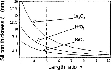
Figure 6. Silicon film thickness vs. γ = LG/λ for double-gate fully-depleted SOI transistors with LG = 13 nm. The vertical dashed line at γ = 5 marks the maximum possible Si thickness tSi to be used with three different gate insulator materials for 22 nm LSTP. For a gate-all-around geometry, the tSi values are doubled.
From these considerations, it seems that SiO2 as a gate insulator will not be suitable for double-gate devices, although it may still work for gate-all-around geometries. For double-gate structures, a dielectric with the properties of La2O3 seems necessary. An interesting observation is that HfO2 might be possible to use for the gate-all-around case if silicon wire dimensions of about 8 nm can be prepared.
5. Conclusions
For a long time, the complicated electric fields occurring under the MOSFET gate have been a key obstacle to downscaling. In order to reach the 22 nm node, new materials and novel geometries are being studied, which pose a number of challenging development problems in the next decade. For bulk devices, it may not be enough to find a high-κ dielectric with sufficient capacitive coupling between gate and semiconductor. To control the potential distribution between source and drain, doping the semiconductor volume for example in a super-halo pattern as suggested in Ref. 9 also appears essential. This requires a precise ion implantation process step, which complicates the process and thus increases production cost.
Multiple-gate SOI structures have long been proposed as superior from this point of view. The estimates presented in this chapter, however, indicate that the same issue of finding a suitable high-κ dielectric exists as for bulk technology. Furthermore, specific new SOI problems crop up due to the need for extremely thin silicon films. This conclusion agrees with investigations carried out by others using similar methods.15
More advanced simulations, in Ref. 3 and 4, have pointed out the possibility of making FD-DGSOI transistors for the 22 nm LSTP node by using silicon dioxide as a gate insulator material. However, in both cases tox was chosen thinner (1.0 and 1.5 nm, respectively) than can satisfy the LSTP requirements set by this node. Furthermore, similar to the present results, the simulations in Ref. 3 lead to a silicon film thickness of 3 nm for a DG MOSFET with 13 nm gate length, again in the risk zone for low intrinsic mobi1ity.19 In Ref. 4, a subthreshold slope close to ideal was found by simulation for a 13 nm device with a silicon film thickness as high as 10 nm. Looking at the material parameters used in this simulation, one finds a natural length λ = 4 nm, resulting in γ = LG/λ ~ 3, which would be expected to give a high DIBL. For the 22 nm node, therefore, SOI technology does not seem to offer a clear advantage compared with that of bulk CMOS.
The results above suggest that changing from bulk CMOS to SOI technology, the gate dielectric problem will mainly be the same while the problem of electric field distribution in the bulk is supplanted by the problem of increased charge carrier scattering in the channel. A convenient but superficial conclusion would be that traditional silicon technology will never reach the 22 nm node within the next ten years, but will instead be replaced by new methods based on for example carbon nanotubes or molecular structures.20 Considering the fact that transistor functionality of 5 nm bulk devices has already been demonstrated,21 even if most technical device requirements have not been fulfilled, it is obvious that silicon technology has a far better point of departure from the present stage than any other. In the history of products based on the MOS transistor, starting in the 1970’s, a decade is a long period of time. The present analysis emphasizes that the drawn-out competition between bulk and SOI technologies will continue, which increases the probability that the MOS transistor concepts of today will survive the next decade.
- H. K. J. Ihantola and J. L. Moll, “Design theory of a surface field-effect transistor,” Solid State Electronics 7, 423 (1964).
- T. Sugii, “High performance bulk CMOS technology for the 65/45 nm node,” Solid State Electronics 50, 2 (2006).
- J. G. Fossum, L. -Q. Wang, J. -W. Yang, S. -H. Kim and V. P. Trivedi, “Pragmatic design of nanoscale multi-gate CMOS,” Tech. Digest IEDM (2003), p. 613.
- L. Risch, “Pushing CMOS beyond the roadmap,” Solid State Electronics 50, 527 (2006)
- H. Iwai and S. Ohmi, “Silicon integrated circuit technology from past to future,” Microelectronics Reliability 42, 465 (2002).
- J. Robertson, “High dielectric constant oxides,” Eur. Phys. J. Appl. Phys. 28, 265 (2004).
- H. Wong and H. Iwai, “On the scaling issues and high-κ replacement of ultrathin gate dielectrics for nanoscale MOS transistors,” Microelectronics Eng. 83, 1867 (2006).
- Y. Taur, C. H. Wann and D. J. Frank, “25 nm CMOS design considerations,” Tech. Digest IEDM (1998), p. 789.
- M. Zhang, J. Knoch, Q. T. Zhao, St. Lenk, U. Breuer, and S. Mantl, “Impact of dopant segregation on fully depleted Schottky-barrier SOI-MOSFETs,” Solid State Electronics 50, 594 (2006).
- ITRS Roadmap, 2004 edition, see http://public.itrs.net
- T. Kauerauf, B. Govoreanu, R. Degraeve, G. Groeseneken, and H. Maes, “Scaling CMOS: Finding the gate stack with the lowest leakage current,” Solid State Electronics 49, 695 (2005).
- O. Engström, B. Raeissi, S. Hall, et al., “Navigation aids in the search for future high-κ dielectrics: Physical and electrical trends,” Proc. 7th Eur. Workshop Ultimate Integr. Silicon (ULIS), Grenoble (2006), submitted to Solid State Electronics.
- H. Iwai, S. Ohmi, S. Akama, et al., “Advanced gate dielectric materials for sub-100 nm CMOS,” Tech. Digest IEDM(2002), p. 625.
- G. K. Celler and S. Cristoloveanu, “Frontiers of silicon-on-insulator,” J. Appl. Phys. 93, 4956 (2003).
- J. -P. Colinge, “Multiple gate SOI-MOSFETs,” Solid State Electronics 48, 897 (2004).
- L. Chang and C. Hu, “MOSFET scaling into the 10 nm regime,” Superlatt. Microstruct. 28, 351 (2000).
- R. -H. Yan, A. Ourmazd, and K. F. Lee, “Scaling Si MOSFET: From bulk to SOI to bulk,” IEEE Trans. Electron Dev. 39, 1704 (1992).
- T. Ernst, D. Munteanu, S. Cristoloveanu, et al., “Investigation of SOI MOSFETs with ultimate thickness,” Microelectronics Eng. 48, 339 (1999).
- L. Donetti, F. Gamiz, J. B. Roldán and A. Godoy, “Acoustic phonon confmement in silicon nanolayers: Effect on electron mobility,” J. Appl. Phys. 100, 013701 (2006).
- B. Yu and M. Meyyappan, “Nanotechnology: Role in emerging nano-electronics,” Solid State Electronics 50, 536 (2006).
- H. Wakabayashi, S. Yamagami, N. Ikezawa, et al., “Sub-10-nm planar-bulk-CMOS devices using lateral junction control,” Tech. Digest IEDM (2003), pp. 989–991; H. Wakabayashi, T. Ezaki, M. Hane, et al., “Transport properties of sub-10-nm planar-bulk-CMOS devices,” Tech. Digest IEDM (2004), pp. 429–432.