
The Future of Single- to Multi-Band Detector Technologies
NASA Langley Research Center, Hampton, VA 23681, U.S.A.
Rensselaer Polytechnic Institute, Troy, NY 12180, U.S.A.
Jet Propulsion Laboratory, Pasadena, CA 91109, U.S.A.
Old Dominion University, Norfolk, VA 23529, U.S.A.
NASA Langley Research Center, Hampton, VA 23681, U.S.A.
1. Introduction
Using classical optical components such as filters, prisms, and gratings to separate the desired wavelengths before they reach the detectors results in complex optical systems composed of heavy components. A simpler approach might rely on a single optical system and a detector that responds separately to each wavelength band. Therefore, the development and fabrication of reliable detector arrays that respond to multiple wavelength regions has been a continuous endeavor. In this chapter, we will review the state-of-the-art single and multicolor detector technologies over a wide spectral range, for use in space-based and airborne remote sensing applications. Our discussion will be focused on current and most recently developed focal plane arrays (FPAs), in addition to emphasizing future development in UV-to-far infrared (IR) multicolor FPA detectors for next generation space-based instruments to measure water vapor and greenhouse gases.
Multi-band detector technology is progressing towards a number of exciting applications, such as remote sensing and imaging, military, and medical imaging. Development of this technology in the UV-to-far infrared region is critical and remains one of the important building blocks for the successful development of active and passive remote sensing. Such novel detectors will make instruments more efficient while reducing complexity and associated electronics and weight.
A multi-band detector consists of a stacked arrangement of different materials in which the shorter wavelength detector is placed top of the longer wavelength detector. The top detector material absorbs only the shorter wavelength radiation and transmits the longer wavelength radiation to the bottom detector. This arrangement is preferable to using lenses, prisms and gratings to separate the individual wavelength before it reaches the detectors.
Mercury cadmium telluride (HgCdTe) and quantum well infrared photodetector (QWIP) technology is expanding from single-color to multicolor detectors. Multicolor detector arrays based on QWIPs have recently been demonstrated.1-3 Development of multi-band arrays will continue4-5 and two-band detectors have been demonstrated based on HgCdTe FPAs.6-10 A joint effort among NASA Langley, JPL, and RPI is developing a multicolor FPA with three-dimensional (3D) structure to provide high-resolution spectroscopy for imaging Fourier-transform interferometers. An increasing interest in multicolor imaging technology is materializing in the UV-to-far IR with the goal of producing large and 3D FPAs.
At present, the availability of multicolor detectors is limited to the 3–15 μm spectral range and no multicolor detector technology has been reported spanning the entire UV-to-far IR spectrum.11,12 The progress in multicolor detector development is driven by the need to detect water vapor and greenhouse gases over a broad wavelength range. This technology will be very valuable to the NASA Earth and Space Science Enterprises and Planetary Exploration Program, allowing critical measurements at improved accuracy with greatly reduced system complexity, weight, and cost. A simpler system would result by utilizing a single optical system and a detector that responds separately to each wavelength band as shown in Fig. 1. The multicolor detector approach is likely to prove useful for several other terrestrial and planetary remote sensing applications.
To achieve the wavelengths either less than 1 μm or greater than 15 μm, one can extend the operating wavelengths by using Si microbolometers and shorten the operating wavelengths by using phosphor coating on Si material.12 However, these approaches face significant technical difficulties. Quaternary layers of GaInAsSb with wavelength longer than 2.5 μm have been grown by metal-organic chemical vapor deposition (MOCVD) with good optical and electrical properties. These layers are lattice-matched to GaSb or InAs substrates with cutoff wavelengths for absorption tailored from 1.7 to 3.5 μm. Epitaxial growth on a lattice-matched substrate is crucial to reducing unwanted defects that could lead to higher noise in the detector. There are at present few materials with varying band gaps that cover the ultraviolet to far IR wavelength band with lattice-matched conditions.
Therefore, a multi-band detector array, sensitive in broadband range with different bands covering the 0.4 μm-to-far IR wavelength range is urgently needed.11,12 To achieve this, we anticipate making use of Si, GaSb, InAs, III-V semiconductor ternary and quaternary alloy-based materials, and of vertically integrated p-i-n heterostructure diodes grown by metal-organic vapor phase epitaxy (MOVPE) with wafer bonding used when necessary. Adding up to 4–5 materials expands the flexibility of the semiconductor material system so that photo-excitation band gaps and lattice parameters can be adjusted independently, allowing us to find a lattice-matched substrate on which to grow these multicolor detector stacks monolithically, or lattice-mismatched detector stacks using wafer bonding technology.
2. Multicolor single element detector structures
The integration of silicon technology with the antimonide-based material system allows for the simultaneous detection of multiple wavelengths in the visible and the IR. The materials of interest – GaSb, AlSb and InAs – are closely lattice-matched, but have widely different bandgaps: GaSb has a bandgap of 0.72 eV, AlSb has an indirect band gap of 1.63 eV, and InAs has a bandgap of 0.356 eV. The lattice constants of these materials are 6.0959Å (GaSb), 6.136Å (AlSb), and 6.0583Å (InAs). There is no perfect lattice match, and hence we can expect a high density of dislocations when one material is grown on the other. However, one can grow ternary and quaternary layers lattice-matched to one of the binaries, and the band gap of the quaternary layers can be tuned to any desired wavelength, still maintaining the lattice-matched condition. This allows great flexibility in device design, but the material growth becomes more complicated. Still, recent advances in MOVPE growth technique can allow reproducible growth of such quaternary layers. Growth of high quality quaternary layers was demonstrated very recently for use in thermophotovoltaic systems.13,14
The multi-wavelength device structure in the UV-to-IR band is shown schematically in Fig. 1. An n-type GaSb substrate is chosen on which a p-on-n InAs device structure is grown, followed by an n-on-p second IR detector in a quaternary layer of InGaAsSb. The band gap of the quaternary layer can be changed from 0.29 eV to 0.35 eV or from 0.7 eV to 0.5 eV (wavelength cut-off from 4.3 to 3.5 μm or from 1.7 to 2.5 μm), while still maintaining the lattice match with the substrate.
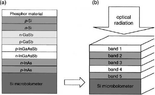
Figure 1. Schematic of multi-layer bias selectable multi-wavelength IR detector: (a) single element layered structures, and (b) 3D focal plane array detector structures.12
One important point to remember in the above structure is the band alignment. The InAs/GaInAsSb heterostructure has a type-II band alignment. In the above configuration, i.e., n-p(InAs)–p-n(GaInAsSb) configuration, the minority carrier electrons in p-GaInAsSb will not be collected by the lower bandgap junction. However, the electrons from the lower bandgap p-type layer can be collected by the common junction, and hence there will be a small amount of crosstalk. Independently biasing the two junctions will alleviate this problem, and in addition, the p-type lower bandgap material thickness should be kept to a minimum to reduce this cross talk further.
We propose to use wafer-bonding approach to overcome the lattice mismatch problem present in ternary layers. This allows us to optimize the detectors for each region of operation and achieve high quantum efficiency. The proposed multi-color detector is based on the integration of Si microbolometer with the Si and the III-V compound-based IR detectors to cover the wavelengths of interest. The IR detector structures used are grown on a GaSb substrate using MOVPE. The composite single detector layered structures are shown in Fig. 1(a).
Figure 1(b) shows the 3D detector sketch with input radiation from the optical system impinging the detector stack. Light of the appropriate wavelengths of interest is absorbed in the first detector in this “sandwich”, while longer wavelengths are passed into the second detector, then the third, etc. The desired absorption wavelengths in each detector can be tailored for each atmospheric or geophysical sounding application. making for a very efficient instrument, as necessary spectral lines or spectral bands are processed.
3. State-of-the-art multicolor focal plane array detector technologies
Many different device structures, such as HgCdTe, GaAs/AIGaAs quantum well photodetectors, strained layer InAs/GaInSb superlattices (SLSs), Schottky barriers on Si, SiGe heterojunctions, pyroelectric detectors, silicon bolometers, and high temperature superconductors are used for the detection of UV-to-far IR radiation. But the bulk single-crystal semiconductor remains the material of choice for efficient detection of electromagnetic radiation in the UV - long wavelength ranges.11
At present, HgCdTe photodiodes and quantum well infrared photoconductors (QWlPs) present multicolor capability in the MWIR–LWIR wavelength range. HgCdTe is based on II-VI and QWlP is based on the well-developed III-V material systems, which have some advantages and disadvantages. HgCdTe FPAs have higher operating temperature, higher quantum efficiency, but lower yield and higher cost. On the other hand, QWIPs are easier to fabricate with high operability, good uniformity, high yield, and lower cost, but have lower quantum efficiency and lower operating temperature. In this section, we discuss the state-of-the-art multicolor detector based on II-VI (HgCdTe), III-V (quantum well) materials, and also future prospects of single-crystal material systems.11
![]() II-VI (HgCdTe) material systems
II-VI (HgCdTe) material systems
There is considerable interest in multispectral HgCdTe detectors employing liquid phase epitaxy (LPE), molecular beam epitaxy (MBE) and metal-organic chemical vapor deposition (MOCVD) for the growth of a variety of devices by research groups at BAE Systems, Hughes Research Laboratory, Rockwell Scientific Company, LETI LIR, SOFRADIR, Raytheon Vision Systems, and AIG AEG INFRAROT.15-26 Devices for the sequential and simultaneous detection of two closely spaced subbands in the MWIR and LWIR ranges have been demonstrated.
An early example of two-color detector is the one described in references,20,21 where an n-p-n three-layer structure in HgCdTe was epitaxially grown on CdTe substrates as shown in Fig. 2. The detector array is illuminated from the backside through the substrate, since CdTe has a bandgap much higher than the wavelengths of interest. The wavelength of interest can be selected by selecting the appropriate bias. This bias-selectable two-color detector affords perfect spatial collocation of the two detectors, but it has inherent drawback of not allowing temporal simultaneity of detection. Either one or the other photodiode is functioning depending on the bias polarity applied across the back-to-back pair. Reine and co-workers15 demonstrated a two-color detector with a four-layer P-N-n-p structure was grown epitaxially on CdTe substrate (the capitalized doping designations refer to the higher bandgap material, i.e. the P-N junction refers to the higher bandgap HgCdTe, whereas the second n-p junction refers to lower bandgap HgCdTe). The signal enters through the substrate and the signal processing electronics is In-bonded to the top surface. This allows independent simultaneous detection of two colors. Two color detection in the 3–5 μm and 8–12 μm ranges was demonstrated, with the layers were grown by MOVPE. The cross-section of the independently accessed back-to-back photodiode dual-band detector is shown in Fig. 3. There are three ohmic contacts in this structure, one to the p-LW layer, one to the n-LW and N-MW layers, and one to the P-MW layer (not shown). The common terminal is the contact to the n-LW and N-MW layer. The p-type regions of all the MW photodiodes in the dual band array are electrically connected and are accessed at the edge of the array through a common array ground contact.
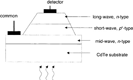
Figure 2. Schematic cross-section of triple-layer bias-selectable dual-wavelength HgCdTe IR detector.20
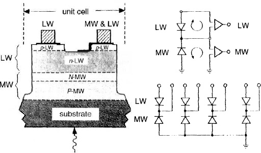
Figure 3. Schematic diagram of dual-band detectors in HgCdTe (from Ref. 6).
The above two-color detectors are possible in HgCdTe since the bandgap of HgCdTe can be continuously varied from 0 to 1.4 eV without any changes in the lattice constant. Hence, it is possible to grow high quality materials with minimum defects on CdTe substrates. Since CdTe has higher bandgap, backside illumination is possible without extra processing steps.
A 64x64 MW/LW dual-band MOCVD HgCdTe array has been demonstrated in Ref. 6 and also discussed in Ref. 22. A unit cell size of 75×75 μm2 of these arrays was hybridized to a dual-band silicon multiplexer readout chip. This allowed the MW and LW photocurrents to be integrated simultaneously and independently. The average cut-off wavelengths of the MW and LW were in the 4.27−4.35 μm and 10.1−10.5 μm ranges at T = 77K, respectively. High average quantum efficiencies of 79% and 67%, high median detectivities of 4.8×1011 cm·√Hz/W and 7.1×1010 cm·√Hz/W, and low median noise equivalent differential temperatures (NEDTs) of 20 mK and 7.5 mK were demonstrated for MW and LW infrared dual-band detector at Tscene = 295 K and f/2.9. Tissot at CEA/LETI27 reported a high performance MWIR two-color detector by superposition of HgCdTe layers with different composition. This two-color detector structure allows simultaneous detection of 3 μm cutoff wavelength for band 1 and 5 μm cutoff wavelength for band 2 radiation in the same pixel. The average resistance R0A values of 107 Ω·cm2 for the band 1 and 4×10⁵ Ω·cm2 for the band 2 diodes at T = 77 K were reported, as well as quantum efficiencies of 75% for band 2 and 50% for band 1 without anti-reflection (AR) coating. The crosstalk between band 1 and 2 was measured to be 2%. Tennant and co-workers19 obtained two-color FPAs with background-limited detectivity performance for band 1 (MWIR: 3–5 μm) devices at T > 130 K and band 2 (LWIR: 8–10 μm) devices at T ~ 80 K. An FPA of 128×128 pixels was fabricated from these devices with 40 μm pixel pitch, with low NEDTs of 9.3 mK for band 1 and 13.3 mK for band 2 – values similar to good quality single-color FPAs. Finally, this group demonstrated 79% of broadband quantum efficiency for band 1 with only a 4% variation over the pixels and 75% for band 2 with a 2% variation over the pixels without AR coating. The authors speculated that the larger variation in band 1 was due to the effect of crosstalk on pixels adjacent to a defective pixel.
Recently, Raytheon Vision Systems developed two-color detectors with MWIR and LWIR cut-off wavelengths of 5.5 μm and 10.5 μm with quantum efficiency >70% for both MW and LW performance at 78 K.9,10 Large 1280×720 MWIR/LWIR FPAs with 20 μm unit cells and 99% pixel operability have been demonstrated, with high-quality simultaneous imaging of the spectral bands achieved by mating the FPA to a readout integrated circuit. Smith and co-workers9,10 have demonstrated large-format megapixel 2048×2948 FPAs with 20 μm unit cells and 2560×512 FPAs with 25 μm unit-cell by using double layer heterojunction HgCdTe growth on Si substrates in the short wavelength infrared (SWIR) and MWIR spectral ranges.
![]() III-V compound material systems
III-V compound material systems
Quantum well infrared photodetectors based on III-V compound materials have been extensively investigated for high-background applications by using large area highly uniform FPAs. This technology holds considerable promise for the fabrication of multicolor FPAs.28-33 Among the different types of QWIPs, GaAs/AlGaAs multiple quantum well detectors are the most mature.34-36 Sundaram and co-workers at BAE Systems demonstrated three separate two-color FPAs with MW/MW (4.0/4.7 μm), MW/LW (5.1/8.5 μm), and LW/LW (8.3/11.2 μm) simultaneous detection.30,37 Typical operating temperature for these QWIP detectors is in the T = 40–100 K range. Peak responsivities of both blue and red QWIPs (LW/LW) are around 320 and 480 mA/W at T = 40 K at an operating bias of −2.0 V; 35 and ~95 mA/W for the blue and red QWIPS (LW/MW) at an operating bias −2.0 V; and ~12 and ~27 mA/W for the blue and red QWIPs (MW/MW) at an operating bias −2.0 V. This group has demonstrated high operability (>99%) and reasonably high peak responsivity in both colors in several different color combinations (MW/MW, MW/LW, LW/LW FPAs). Large format single-color 640×480 pixel QWIP FPAs with 22 μm squares on 24 μm centers, giving a fill factor of 84%, were fabricated by BAE Systems for U.S. Army Research Laboratory (ARL). Goldberg and co-worker38,39 at ARL also demonstrated the potential of dual-band MWIR/LWIR imaging (developed by BAE Systems) for tactical environments by the application of a color image-fusion technique. Recently, Goldberg and co-workers31 presented results of a large-format megapixel 1024×1024 QWIP FPA, which was produced by QWIP Technologies, Inc. This device was tested at the ARL and results obtained including conversion efficiency close to 10%, the spectral response peak at 8.55 μm, and a dark current level low enough to allow background-limited infrared performance (BLIP) at 76 K.
Gunapala and co-workers28 have demonstrated LWIR and very LWIR (8–9 and 14–15 μm) two-color imaging camera based on a 640×486 dual-band QWIP FPAs. This dual-band QWIP device can be processed into simultaneously readable dual-band FPAs with triple contacts to access the CMOS readout multiplexer40 or interlace readable dual-band FPA (i.e., odd rows for one color and the even rows for the other color). The first approach requires a special dual-band readout multiplexer that contains two readout cells per detector unit cell, whereas the second approach needs only a single-color readout multiplexer. The advantages of this scheme are that it provides simultaneous data readout and allows the use of currently available single-color CMOS readout multiplexers. However, the disadvantage is that it does not provide a full fill factor for both wavelength bands. The device structure, shown in Fig. 4,22,28 consists of a 30 period stack (500 Å AlGaAs barrier and a 60 Å GaAs well) of VLWIR structure and a second 18 period stack (500 Å AlGaAs barrier and a 40 Å GaAs well) of LWIR structure, separated by a heavily-doped 0.5 μm thick intermediate GaAs contact layer. The VLWIR QWIP structure has been designed to have a bound-to-quasibound intersubband absorption peak at 14.5 μm, whereas the LWIR QWIP structure has been designed to have a bound-to-continuum intersubband absorption peak at 8.5 μm, since photocurrent and dark current of the LWIR device structure is relatively small compared to the VLWIR portion of the device structure. The performance of dual-band FPAs has been tested at a background temperature of 300 K, with f/2 cold stop, and at 30 Hz frame rate and are discussed in Ref. 30. The mean values of quantum efficiency at operating T = 40 K and −2V bias are 12.9% and 8.9% in LW and VLW spectral range, respectively. The estimated NEDTs of LWIR and VLWIR detectors at 40 K are 36 and 44 mK, respectively. Recently, Gunapala and co-worker32,33 demonstrated MWIR and LWIR 1024×1024 pixel QWIP FPAs with excellent imaging performance. The MWIR and LWIR prototype cameras with similar optics have shown BLIP performance at operating T = 90 K and 70 K respectively, at 300 K background.
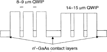
Figure 4. Conduction band energy diagram of the long-wavelength two-color infrared detector. The long-wavelength (8–9 μm) sensitive multiquantum well stack utilizes the bound-to-continuum intersubband absorption. The very long-wavelength (14–15 μm) stack utilizes the bound-to-quasibound intersubband absorption.28

Figure 5. JPL completed a four-color 640×512 imaging focal plane array (3–15 μm) for the hyperspectral QWIP imaging system.1
A joint effort between Goddard Space Flight Center, Jet Propulsion Laboratory, and ARL demonstrated a four-band, hyperspectral 640×512 QWIP array for the NASA Earth Science mission.1,41 Recently, Bandara and co-workers2,3 have reported remarkable progress in realizing large-format multi-band and broadband FPAs. These QWIP FPAs have been developed for an imaging interferometer based on the InGaAs/GaAs/AIGaAs material system. The spectral range is from 3 to 15.4 μm. This FPA consists of four independently readable IR bands: (1) 3–5 μm, (2) 8.5–10 μm, (3) 10–12 μm, and (4) 14–15.4 μm. Each band occupies a 640×128 pixel area within the single imaging array. Figure 5 illustrates the conceptual design and spectral response of the four-band multiquantum well QWIP.1
Most recently, NASA Langley Research Center with partnerships at RPI and JPL proposed to develop the technical capability to reliably fabricate detector arrays that respond to multiple wavelength regions.11,12 We plan to use epitaxial growth followed by wafer bonding to overcome the lattice mismatch problem. This will allow us to optimize the detectors for each region of operation to achieve high quantum efficiency. The proposed multicolor detector will be based on the integration of silicon detectors with the antimonide-based IR detectors to cover the wavelengths of interest. The IR detector structures will be grown on GaSb or InAs substrates by MOVPE and these detector structures will be transferred to the silicon substrates using wafer bonding technology. The composite single-element detector structure is shown in Fig. 1.
4. Conclusions
Multicolor detector technology is rapidly advancing towards a number of exciting applications, such as remote sensing and imaging, military, and medical imaging. HgCdTe and QWIP technology is expanding from single-band to multi-band detectors and, recently, QWIPs have been integrated into multi-band detector arrays. Development of multi-band arrays will continue and three-band detectors will be soon demonstrated based on HgCdTe FPAs. A joint effort between NASA Langley, RPI, and JPL is currently working on a multi-band FPA with 3D structure to provide high-resolution spectroscopic imaging for military, medical, hyperspectral and Fourier-transform interferometers. An increasing interest in multi-band imaging technology is materializing in the UV-to-far IR with the feasibility of focal planes founded on large and three-dimensional arrays.
References
- S. V. Bandara, S. D. Gunapala, J. K. Liu, et al., “Four-band quantum well infrared photodetector array,” Infrared Phys. Technol. 44, 369 (2003).
- S. V. Bandara, S. Gunapala, C. Hill, et al., “Multi-band infrared detectors based on III-V materials,” Proc. SPIE 5543, 1 (2004).
- S. V. Bandara, S. D. Gunapala, J. K. Liu, et al., “Multi-band and broad-band infrared detectors based on III-V materials for spectral imaging instruments,” Infrared Phys. Technol. 47, 15 (2005).
- L. Becker, “Multicolor LWIR focal plane array technology for space and ground based applications,” Proc. SPIE 5564, 1 (2004).
- A. K. Sood, J. E. Egerton, Y. R. Puri, et al., “Design and development of multicolor MWIR/LWIR and LWIR/VLWIR detector arrays,” J. Electron. Mater. 34, 909 (2006).
- M. B. Reine, A. Hairston, P. O’Dette, et al., “Simultaneous MW/LW dual-band MOCVD HgCdTe 64×64 FPAs,” Proc. SPIE 3379, 200 (1998).
- E. Smith, L. Pham, G. Venzor, et al., “Two-color HgCdTe infrared staring focal plane arrays,” Proc. SPIE 5209, 1 (2003).
- J. Giess, M. A. Glover, N. T. Gordon, et al., “Dual-waveband infrared focal plane arrays using MCT grown by MOVPE on Si substrate,” Proc. SPIE 5783, 316 (2005).
- E. P. G. Smith, E. A. Patten, P. M. Goetz, et al., “Fabrication and characterization of two-color mid-wavelength/long-wavelength HgCdTe infrared detectors,” J. Electron. Mater. 35, 1145 (2006).
- E. P. G. Smith, R. E. Bornfreund, I. Kasai, et al., “Status of two-color and large format HgCdTe FPA technology at Raytheon Vision Systems,” Proc. SPIE 6127, 61271F-1(2006).
- M. N. Abedin, T. F. Refaat, J. M. Zawodny, et al., “Multicolor focal plane array detector: A review,” Proc. SPIE 5152, 279 (2003).
- M. N. Abedin, T. F. Refaat, Y. Xiao, and I. Bhat, “Characterization of dual-band infrared detectors for application to remote sensing,” Proc. SPIE 5883, 588307-1 (2005).
- C. Hitchcock, R. Gutmann, J. Borrego, I. Bhat, and G. Charache, “Antimonide based devices for thermophotovoltaic applications,” IEEE Trans. Electron Dev. 46, 2154 (1999).
- C. A. Wang, H. K. Choi, and S. L. Ransom, “High-quantum-efficiency 0.5 eV GaInAsSb/GaSb thermophotovoltaic devices,” Appl. Phys. Lett. 75, 1305 (1999).
- M. B. Reine, P. W. Norton, R. Starr, et al., “Independently accessed back-to-back HgCdTe photodiodes: A new dual-band infrared detector,” J. Electron. Mater. 24, 669 (1995).
- R. D. Rajavel, P. D. Brewer, D. M. Jamba, et al., “Status of HgCdTe-MBE technology for producing dual-band infrared detectors,” J. Crystal Growth 214/215, 1100 (2000).
- S. M. Johnson, J. L. Johnson, W. J. Hamilton, et al., “HgCdZnTe quaternary materials for lattice matched two-color detectors,” J. Electron. Mater. 29, 680 (2000).
- W. E. Tennant, M. Thomas, L. J. Kozlowski, et al., “A novel simultaneous unipolar multispectral integrated technology approach for HgCdTe IR detectors and focal plane arrays,” J. Electron. Mater. 30, 590 (2001).
- P. Ferret, J. P. Zanatta, R. Hamelin, S. Cremer, A. Million, M. Wolny, and G. Destefanis, “Status of the MBE technology at LETI LIR for the manufacturing of HgCdTe focal plane arrays,” J. Electron. Mater. 29, 641 (2000).
- K. Kosai, “Status and application of HgCdTe device modeling,” J. Electron. Mater. 24, 635 (1995).
- E. R. Blazejewski, J. M. Arias, G. M. Williams, W. McLevige, M. Zandian, and J. Pasko, “Bias-switchable dual-band HgCdTe infrared photodetector,” J. Vac. Sci. Technol. B 10, 1626 (1992).
- A. Rogalski, “Infrared detectors: An overview,” Infrared Phys. Technol. 43, 187 (2002).
- J. Baylet, P. Ballet, P. Castelein, et al., “TV/4 dual-band HgCdTe infrared focal plane arrays with a 25-micron pitch and spatial coherence,” J. Electron. Mater. 35, 1153 (2006).
- P. Tribolet and G. Destefanis, “Third generation and multi-color IRFPA development: A unique approach based on DEFIR,” Proc. SPIE 5783, 350 (2005).
- W. A. Radford, E. A. Patten, D. F. King, et al., “Third generation FPA development status at Raytheon Vision Systems,” Proc. SPIE 5783, 331 (2005).
- R. Breiter, W. Cabanski, K.-H. Mauk, W. Rode, J. Ziegler, H. Schneider, and M. Walther, “Multicolor and dual-band IR camera for missile warning and auto-matic target recognition,” Proc. SPIE 4718, 280 (2002).
- J. L. Tissot, “Advanced IR detector technology development at CEA/LETI,” Infrared Phys. Technol. 43, 223 (2002).
- S. D. Gunapala, S. V. Bandara, A. Singh, et al., “8–9 and 14–15-micron two-color 640×486 quantum well infrared photodetector (QWIP) focal plane array camera,” Proc. SPIE 3698, 687 (1999).
- P. Bois, E. Costard, X. Marcadet, and E. Herniou, “Development of quantum well infrared photodetectors in France,” Infrared Phys. Technol. 42, 291 (2001).
- M. Sundaram, S. C. Wang, M. F. Taylor, et al., “Two-color quantum well infrared photodetector focal plane arrays,” Infrared Phys. Technol. 42, 301 (2001).
- A. Goldberg, K. K. Choi, E. Cho, and B. McQuiston, “Laboratory and field performance of megapixel QWIP focal plane arrays,” Infrared Phys. Technol. 47, 91 (2005).
- S. D. Gunapala, S. V. Bandara, J. K. Liu, et al., “Development of mid-wavelength and long-wavelength megapixel portable QWIP imaging cameras,” Infrared Phys. Technol. 47, 67(2005).
- S. D. Gunapala, S. V. Bandara, J. K. Liu, et al., “1024×1024 pixel MWIR and LWIR QWIP focal plane arrays and 320×256 MWIR:LWIR pixel collocated simultaneous dualband QWIP focal plane arrays,” Proc. SPIE 5783, 789 (2005).
- B. F. Levine, “Quantum well infrared photodetectors,” J. Appl. Phys. 74, RI (1993)
- Y. Zhang, D. S. Jiang, J. B. Xia, L. Q. Cui, C. Y. Song, Z. Q. Zhou, and W. K. Ge, “A voltage-controlled tunable two-color infrared photodetector using GaAs/AIAs/GaAIAs and GaAs/GaAIAs stacked multiquantum wells,” Appl. Phys. Lett. 68, 2114 (1996).
- A. Rogalski, “Assessment of HgCdTe photodiodes and quantum well infrared photodetectors for long wavelength focal plane arrays,” Infrared Phys. Technol. 40, 279 (1999).
- M. Sundaram and S. C. Wang, “2-color QWIP FPAs,” Proc. SPIE 4028, 311 (2000).
- A. Goldberg, T. Fischer, S. Kennerly, W. Beck, V. Ramirez, and K. Garner, “Laboratory and field imaging test results on single-color and dual-band QWIP focal plane arrays,” Infrared Phys. Technol. 42, 309 (2001).
- A. C. Goldberg, S. W. Kennerly, J. W. Little, et al., “Comparison of HgCdTe and QWIP dual-band focal plane arrays,” Proc. SPIE 4369, 532 (2001).
- S. D. Gunapala, S. V. Bandara, A. Singh, et al., “Quantum well infrared photo-detectors for low background applications,” Proc. SPIE 3379, 225 (1998).
- M. Jhabvala, “Application of GaAs quantum well infrared photoconductors at the NASA/Goddard Space Flight Center,” Infrared Phys. Technol. 42, 363 (2001).