
Fermi Liquid Behavior of GaAs Quantum Wires
School of Physics and Astronomy, Tel Aviv University, Tel Aviv 69978, Israel
Ecole Polytechnique Federale de Lausanne (EPFL)
CH-1015 Lausanne, Switzerland
Dept. of Condensed Matter Physics
The Weizmann Institute of Science, Rehovot 76100, Israel
1. Introduction
The electrical conductance through noninteracting clean quantum wires containing a number of one-dimensional subbands is quantized in the universal units 2e2/h.1,2 As the number of the subbands is changed, the conductance varies in a step-like manner (with the plateaus at integer values of the universal unit), as was observed in narrow constrictions in 2D electron gas (2DEG) system.3,4 Typically, the size of the constrictions is comparable to the Fermi length λF, and is much shorter than the mean free path in the 2DEG. For such short and clean narrow wires, the electron-electron interactions described by the so-called Luttinger liquid (LL) model5 do not affect the value of the conductance, namely it is temperature and length independent, as indeed was shown experimentally.3,4 In the presence of disorder suppression of the conductance is expected at low temperatures in sufficiently long quantum wires (QWRs) containing at least a few electrons. A number of theoretical papers6-9 predicted a negative correction to the conductance temperature dependence G(T), which obeys a Tg-1 power law, where g < 1 is an interaction parameter. Eventually, at T = 0, the above theories predict a vanishing conductance. However, these theories all use a perturbation treatment of the disorder and are thus limited to the cases of relatively small disorder. No theoretical treatment beyond perturbation theory has been suggested so far.
The validity of the implications arising from the LL theory has been recently demonstrated in a number of experiments.10, 11 The most clear-cut proof of the theoretical predictions were shown in the tunneling experiments performed in T-shaped cleaved-edged overgrown GaAs quantum wires10 and in carbon nanotubes.11 Earlier non-tunneling experiments, in which suppression of conductance occurs in the linear response regime, did not unambiguously confirm the validity of the theory, and the value of the g parameter could not be deduced from the experimental data.12–14 Several complications are encountered in such experiments. For sufficiently disordered wires, where the correction to the conductance G(T) is expected to be large, the value of the conductance at the plateau is not well defined due to the specific realization of the disordered potential in the wire, as was the case for the long wires of Tarucha et al.12 Moreover, in the intermediate regime, namely, for the disorder level for which the plateau could be well defined but the corrections to G(T) are already significant for a relatively narrow temperature range, the parameter g cannot be extracted by applying perturbation theory. The attempt to extract g from such samples by applying the theory in the limit of weak disorder results in reduced values of g, as we believe was the case in Ref. 14. If, however, the disorder is very weak so that the plateaus are well defined at all temperatures,12,13 the variation of its value vs. temperature is so weak that the g parameter cannot be reliably determined. Therefore, if one wishes to compare G(T) to the theory, a wire possessing just the right amount of disorder is needed in order to avoid the above difficulties. On one hand, the disorder should be weak enough to give well defined plateaus, while on the other hand, the overall weak variation of G(T) should be observed over an extended temperature range so that the perturbation theory could be applied.
In this chapter, we present an experimental study of the conductance in single mode GaAs QWRs grown on a V-groove substrate. The variation of the conductance was measured over a wide temperature range. Our results are consistent with the theories8,9 based on the LL model for weakly disordered wires, allowing us to deduce the value of g = 0.66, as expected for interacting electrons in GaAs and as was observed experimentally in tunneling experiments.10 We show results coming from QWRs displaying varying amounts of disorder, thus enabling us to elucidate the importance of the degree of disorder in fitting to perturbation theory and to show its limits.
2. Sample preparation and the experimental setup
The QWRs studied in this chapter were produced by self-ordered growth of GaAs/AlGaAs heterostructures, using low pressure (20 mbar) metalorganic vapor phase epitaxy (MOVPE) on undoped (001) GaAs substrates with a few isolated V-grooves oriented in the [01![]() ] direction, fabricated by electron-beam and UV lithography, followed by wet chemical etching.15 The heterostructure consisted of a 230 nm GaAs buffer layer, followed by a 1 μm thick Al0.27Ga0.73As layer. The carriers are supplied to the quantum well from 20 nm Si-doped (≈1×1018 cm-3) Al0.27Ga0.73As layers on both sides of the GaAs quantum well layer, spaced by 80 and 60 nm, respectively, in the growth order. The quoted thicknesses are “nominal”, as calibrated on a planar (100) sample. Figure l(a) shows a cross-sectional TEM image of the QWR region of a typical sample used in our experiments. We observe that the thickness of the quantum well varies along the direction perpendicular to the plane, thus strengthening the confinement. In this way, the QWR is formed at the bottom of the V-groove. For the transport measurements, multiple contact samples were fabricated using standard photolithography techniques with a mesa etched along the QWR and with Au/Ge/Ni ohmic contacts, as shown in Fig. 1(b). Additionally, narrow (0.5 μm) Ti/Au Schottky gates were formed using electron beam lithography in order to isolate the QWR and control the number of 1D subbands in it.
] direction, fabricated by electron-beam and UV lithography, followed by wet chemical etching.15 The heterostructure consisted of a 230 nm GaAs buffer layer, followed by a 1 μm thick Al0.27Ga0.73As layer. The carriers are supplied to the quantum well from 20 nm Si-doped (≈1×1018 cm-3) Al0.27Ga0.73As layers on both sides of the GaAs quantum well layer, spaced by 80 and 60 nm, respectively, in the growth order. The quoted thicknesses are “nominal”, as calibrated on a planar (100) sample. Figure l(a) shows a cross-sectional TEM image of the QWR region of a typical sample used in our experiments. We observe that the thickness of the quantum well varies along the direction perpendicular to the plane, thus strengthening the confinement. In this way, the QWR is formed at the bottom of the V-groove. For the transport measurements, multiple contact samples were fabricated using standard photolithography techniques with a mesa etched along the QWR and with Au/Ge/Ni ohmic contacts, as shown in Fig. 1(b). Additionally, narrow (0.5 μm) Ti/Au Schottky gates were formed using electron beam lithography in order to isolate the QWR and control the number of 1D subbands in it.
The conductance of the wire was measured using a four-terminal ac method and lock-in amplifier detection (schematically shown in Fig. 1(b)). If the 2DEG is not depleted in the sidewalls, the electronic transport in our system is carried by both the electrons in the 2D sidewalls and in the 1D quantum wire in parallel. By applying negative voltage to the Schottky gate deposited on top of the mesa, one can fully deplete the 2DEG in the sidewalls and thus isolate a section in which there are electrons only in the 1D wire.16 Over a certain range of the negative gate voltage, a single populated 1D channel is realized. It would be natural to think that the length of the 1D region is determined by the width of the gate. However, as was demonstrated in our previous experiments,17 the electrons remain in their one-dimensional state over a transition length Δ on both sides of the gate – see Fig. 1(b). This transition length arises from the poor coupling between the 1D states and the 2DEG that acts as an electron reservoir and is found to be as large as Δ = 2 μm. From the above discussion it is reasonable to conclude that the effective length of the 1D wire (although not accurately defined) markedly exceeds the actual width of the gate (0.5 μm).
3. Experimental results
Figure 2 shows the variation of the conductance with gate voltage VG, in the range where electrons populate only a single 1D subband, at temperatures between 100 mK and 4.2 K. The electronic temperature of GaAs 2DEG does not deviate from the bath temperature for T > 100 mK, as shown in our previous studies.18 The data were taken at stabilized temperatures of the bath while the VG was swept through the entire range. A series resistance of 180 Ω, measured at VG = 0, has been subtracted from all curves. At T = 4.2 K, the conductance plateau is smooth with G = 0.94(2e2/h), indicating that only weak disorder is present in our samples. At lower temperatures, some small undulations of the conductance values appear on the plateau, but its average value is well defined with the standard deviation being much less than the average value (see error bars in Figs. 3 and 4). A similar phenomenon, namely the appearance of such structures at lower temperatures and their disappearance at higher temperatures, was also recently observed in clean cleaved-edged overgrown wires.19 The variation of the plateau value (approximately 20%) through the wide temperature range (1.5 decades), allows us to make a meaningful comparison of the data to the theories derived in the appropriate limit of weak disorder. Figure 3 shows the measured variation of conductance versus temperature.

Figure 1. (a) Cross-sectional TEM image of the QWR region, on which the charge distribution due to the doping is schematically shown. (b) Top and perspective schematic views of the device’s geometry. The QWR is present at the bottom of the V-groove aligned with the mesa structure.
Early theories, particularly those of Kane and Fisher6 (and of Ogata and Fukuyama7), proposed that for relatively small barriers (weak disorder, which is assumed to result in relatively small corrections), the conductance of a sufficiently long, single-mode 1D spin-full Luttinger liquid system decreases with temperature in the manner
Here, g < 1 is a dimensionless parameter, which is a measure of the strength of the interactions. For repulsive interactions, g obtains roughly from the expression g2 = [1 + (U/2EF)]-l, where U is the Coulomb interaction energy between neighboring electrons. The parameter T0 in Eq. (1) describes the strength of the backscattering (disorder) in the wire; at T ~ T0, the corrections to G(T) become of order (2e2/h). Both theories predict a correction of g(2e2/h) even for ballistic wires at relatively high temperatures. These imply that for sufficiently long wires, one cannot observe values close to 2e2/h in GaAs, since the value of g is expected to be ~0.7 in such wires, as was already pointed out by Tarucha et al.12

Figure 2. Conductance vs. gate voltage VG for 0.5 μm gate width at various temperatures, after subtraction of series resistance.
This contradiction was also addressed in detail in several theoretical papers.8,9,20-22 According to the theory of Maslov,9 the interaction parameter g of the wire determines the exponent of the temperature variation, whereas the pre-factor g in Eq. (1) should be set to one (for non-interacting reservoirs). Figure 3 shows the curve calculated from this modified equation (dashed line).
A different but numerically equivalent result was derived by Oreg and Finkel’stein.9 They also demonstrated that for an infinite clean wire, the conductance keeps the universal value 2e2/h per mode, even in the presence of interactions. According to their theory, because of the electric field renormalization by the interactions, the results given by Kane and Fisher5 of Eq. (1) are modified in the following way:
As can be easily verified, the leading term in the temperature variation of the conductance of Eq. (2) leads to the same results given by Maslov.8 As one can see from Fig. 3, an excellent fit is obtained for both theories,8,9 and we obtain g = 0.64±0.05, as is expected for electrons in GaAs wires. Indeed, this value is consistent with the experiments in Ref. 10, showing g values between 0.66 and 0.82. Moreover, using the Fermi energy EF ≈ 1.5±0.5 meV (half of level spacing between 1D subbands estimated in our previous experiments16) we calculate the corresponding electron densities at the middle of the plateau, obtaining n1D = 3.2±0.5×105 cm-1. Substituting the above value for n1D into U = (e2/ε)n1D we obtain U = 3.85±0.60 meV which yields the values of g = 0.66±0.04, consistent with our fit to the LL model.

Figure 3. Conductance values of the first plateau vs. temperature in the wire of Fig. 2 (points with error bars). Both theoretical expressions are plotted for the same parameters, e.g. g = 0.64 and T0 = 0.7 mK of Eq. (2).
Disorder in V-groove QWRs stems mainly from interface roughness brought about by lithography imperfections on the patterned substrate and peculiar faceting taking place during MOVPE on a nonplanar surface.23 The disorder results in potential fluctuations along the axis of the wire, and manifests itself in localization of excitons and other charge carriers as evidenced in optical spectroscopy studies of these wires.24 Optical and structural studies indicate the formation of localizing potential wells along the wires with size in the range of several tens of nm.25 The specific features of the disorder in the QWRs studied here, in terms of depth and size of the localization potential, are expected to vary from sample to sample. In fact, the degree of disorder is represented in our analysis of the temperature dependence of the conductance by the parameter T0. Repeating the analysis of Fig. 3 for several samples, we observed similar values of g in all the wires characterized by a small amount of disorder (T0 < 2 mK), namely g = 0.66. However, other wires with stronger disorder (T0 > 2 mK), showed lower values of g, around g = 0.5. Figure 4 summarizes the values of g vs. T0, obtained for our different wires.
The values of the total change in ΔG/G were calculated for each wire in the 0.1–4.2 K temperature range and are also shown in Fig. 4. Note that there is a complete correspondence between the two indicators for the strength of the disorder, T0 and ΔG/G.
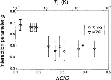
Figure 4. Interaction parameter g vs. disorder parameter T0 and the values of ΔG/G (in the temperature range 0.1–4.2 K). The star represents an estimate for the strength of the disorder for the results reported in Ref. 14. The wrong values of g ≈ 0.5 (at high disorder) are established by using the perturbation formula in a region where it is inapplicable.
The transition between g = 0.66 and g = 0.5 at T0 ≈ 2 mK occurs for ΔG/G ≈ 23%. We believe that above T0 ≈ 2 mK the disorder in the wires is strong enough so that the description by perturbation theory is no longer valid. Trying to fit such data with perturbation-theory equations gives inevitably lower (and wrong) values of g. For such wires, one should use other theories, appropriate to stronger disorder due to many impurities,25 or stronger backscattering26 in the system. The results of conductance measurements in GaAs wires reported recently by Rother et al.14 also correspond to highly disordered samples, and also give g = 0.5. Indeed, analyzing their data, we estimate the value of T0 ≈ 15 mK (marked by a star in Fig. 4) and the change in the conductance ΔG/G ≈ 10% over a small temperature range (1–3 K). These values are even larger than corresponding values for our most disordered sample in the same temperature range.
It is highly unlikely that the observed temperature dependence could be attributed to the contact resistance between the 2DEG and the 1D subbands outside the gated region for the reasons outlined below:
i) if the contact resistance is treated quantum mechanically,13 as a change of the transmission from the 2DEG to the 1D subbands in the ungated region, we would expect that ΔG/G would be similar for any number of 1D channels under the gate. However, we observe that ΔG1/G1 of the first plateau is much smaller than ΔG2/G2 of the second plateau over the same temperature range. This is consistent with the expected result of the Luttinger model where the scattering occurs in the gated region, since the effect of the Coulomb interaction on the transmission depends on the number of 1D subbands. Indeed, from an analysis of higher steps in the conduction depletion curve, used in a smaller temperature range (0.1–0.6 K, where the plateaus are better resolved), we deduce the values g = 0.55 and g = 0.47 for the second and the third plateaus, respectively, which agrees with the theoretical values of 0.54 and 0.47.9
ii) if the decrease of the conductance is considered as an additional contact resistance added in series to the wire (i.e. treated classically), than the values of the transmission for each channel at low T at the second plateau would increase with lowering temperature and eventually exceed unity for each channel. Therefore, we conclude that the observed decrease of the conductance is due to the interactions in the LL model.
4. Conclusions
In conclusion, we have measured the temperature dependence of the electrical conductance in single mode quantum wires. We find that our data is consistent with theoretical calculations8,9 based on the LL model, in the limit of weak disorder in the system. We showed that the use of the perturbative result (namely G′ ![]() Tg-1) in order to estimate g, is valid only for wires produced with a moderate amount of disorder (T0 < 1 mK).
Tg-1) in order to estimate g, is valid only for wires produced with a moderate amount of disorder (T0 < 1 mK).
Acknowledgments
We thank Dganit Meidan for constructive discussions of our results. This research was partially supported by the Israel Science Foundation, founded by the Israeli academy Sciences and Humanities Centers of Excellence Program and by ISF grant 845/04.
References
- R. Landauer, “Spatial variation of currents and fields due to localized scatterers in metallic conduction,” IBM J. Res. Develop. 32, 306 (1988).
- C. W. J. Beenakker and H. van Houten, Quantum Transport in Semiconductor Nanostructures, Vol. 44 in: H. Ehrenreich and D. Turnbull, eds., Solid State Physics series, New York: Academic Press, 1991.
- B. J. van Wees, H. van Houten, C. W. J. Beenakker, et al., “Quantized conductance of point contacts in a two-dimensional electron gas,” Phys. Rev. Lett. 60, 848 (1988).
- D. A. Wharam, T. J. Thornton, R. Newbury, et al., “One-dimensional transport and the quantisation of the ballistic resistance,” J. Phys. C 21, L209 (1988).
- S. Tomonaga, “Remarks on Bloch’s method of sound waves applied to many-fermion problems,” Prog. Theor. Phys. 5, 544 (1950).
- C. L. Kane and M. P. A. Fisher, “Transmission through barriers and resonant tunneling in an interacting one-dimensional electron gas,” Phys. Rev. B 46, 15233 (1992).
- M. Ogata and H. Fukuyama, “Collapse of quantized conductance in a dirty Tomonaga-Luttinger liquid,” Phys. Rev. Lett. 73, 468 (1994).
- D. L. Maslov, “Transport through dirty Luttinger liquids connected to reservoirs,” Phys. Rev. B 52, R14368 (1995).
- Y. Oreg and A. M. Finkel’stein, “dc transport in quantum wires,” Phys. Rev. B 54, R14265 (1996).
- O. M. Auslaender, A. Yacoby, R. de Picciotto, K. W. Baldwin, L. N. Pfeiffer, and K.W. West, “Experimental evidence for resonant tunneling in a Luttinger liquid,” Phys. Rev. Lett. 84, 1764 (2000).
- M. Bockrath, D. H. Cobden, J. Lu, et al., “Luttinger-liquid behavior in carbon nanotubes,” Nature 397, 598 (1999).
- C. Tarucha, T. Honda, and T. Saku, “Reduction of quantized conductance at low temperatures observed in 2 to 10 μm-long quantum wires,” Solid State Commun. 94, 413 (1995).
- A. Yacoby, H. L. Stormer, N. S. Wingreen, L. N. Pfeiffer, K. W. Baldwin, and K. W. West, “Nonuniversal conductance quantization in quantum wires,” Phys. Rev. Lett. 77, 4612 (1996).
- M. Rother, W. Wegscheider, M. Bichler, and G. Abstreiter, “Evidence of Luttinger liquid behavior in GaAs/AlGaAs quantum wires,” Physica E 6, 551 (2000).
- F. Gustafsson, F. Reinhardt, G. Biasiol, and E. Kapon, “Low-pressure organometallic chemical vapor deposition of quantum wires on V-grooved substrates,” Appl. Phys. Lett. 67, 3673 (1995).
- D. Kaufman, Y. Berk, B. Dwir, A. Rudra, A. Palevski, and E. Kapon, “Conductance quantization in V-groove quantum wires,” Phys. Rev. B 59, R10433 (1999).
- D. Kaufman, B. Dwir, A. Rudra, I. Utke, A. Palevski, and E. Kapon, “Direct evidence for quantum contact resistance effects in V-groove quantum wires,” Physica E 7, 756 (2000).
- M. Eshkol, E. Eisenberg, M. Karpovski, and A. Palevski, “Dephasing time in a two-dimensional electron Fermi liquid,” Phys. Rev. B 73, 115318 (2006).
- R. de Picciotto, L. N. Pfeiffer, K. W. Baldwin, and K. W. West, “Nonlinear response of a clean one-dimensional wire,” Phys. Rev. Lett. 92, 036805 (2004).
- D. L. Maslov, and M. Stone, “Landauer conductance of Luttinger liquids with leads,” Phys. Rev. B 52, R5539 (1995).
- I. Safi and H. J. Schulz, “Transport in an inhomogeneous interacting one-dimensional system,” Phys. Rev. B 52, R17040 (1995).
- Y. Oreg and A. M. Finkel’stein, “Interedge interaction in the quantum Hall effect,” Phys. Rev. Lett. 74, 3668 (1995).
- F. Lelarge, T. Otterburg, D. Y. Oberli, A. Rudra, and E. Kapon, “Origin of disorder in self-ordered GaAs/AlGaAs quantum wires grown by OMVPE on V-grooved substrate,” J. Crystal Growth 221, 551 (2000).
- F. Vouilloz, D. Y. Oberli, F. Lelarge, B. Dwir, and E. Kapon, “Observation of many-body effects in the excitonic spectra of semiconductor quantum wires,” Solid State Commun. 108, 945 (1998).
- D. Y. Oberli, M.-A. Dupertuis, F. Reinhardt, and E. Kapon, “Effect of disorder on the temperature dependence of radiative lifetimes in V-groove quantum wires,” Phys. Rev. B 59, 2910 (1999); T. Otterburg, D. Y. Oberli, M.-A. Dupertuis, et al., “Enhancement of the binding energy of charged excitons in disordered quantum wires,” Phys. Rev. B 71, 033301 (2005).
- I. V. Gornyi, A. D. Mirlin, and D. G. Polyakov, “Dephasing and weak localization in disordered Luttinger liquid,” Phys. Rev. Lett. 95, 046404 (2005).
- P. Fendley, A. W. W. Ludwig, and H. Saleur, “Exact nonequilibrium transport through point contacts in quantum wires and fractional quantum Hall devices,” Phys. Rev. B 52, 8934 (1995).