
A New Class of Semiconductors Using Quantum Confinement of Silicon in a Dielectric Matrix
ARC Photovoltaics Centre of Excellence
University of New South Wales, Sydney 2052, Australia
1. Introduction
For photovoltaic use, control of the semiconductor bandgap is important for high energy conversion efficiency designs, such as those based on tandem stacks of cells responding to different spectral ranges. Traditionally, such bandgap control has been obtained using alloys of III-V semiconductors or by Si/Ge alloys in the case of amorphous material. This chapter explores the use of quantum confinement to produce high bandgap material within the crystalline silicon materials system. The optical and transport properties of a new form of synthesized material involving silicon quantum dots in a dielectric matrix of silicon oxide, nitride or carbide are described. These materials may have applications in areas other than photovoltaics where low mobility is tolerable.
The photovoltaics industry is currently booming, with annual sales growing at over 40%/year. This growth is expected to continue into the next decade.1 Most solar sells are based on silicon wafers similar to those used in microelectronics. In 2006, a turning point was reached where the volume of silicon used in photovoltaics exceeded that used in microelectronics for the first time. Traditional polysilicon suppliers are now rapidly increasing capacity to meet the rapidly increasing demand.1 With over 2 gigawatts of new capacity expected to be installed in 2006, new annual capacity additions of photovoltaics will exceed those of nuclear plants within the next year or two.
However, to wean the world from coal as a way of meeting spiralling power demand, photovoltaic costs have to decrease significantly. A transition from wafers to a stable, durable thin-film technology would improve prospects for such a large cost reduction. Incorporating high efficiency features into these thin films, e.g. by using tandem stacks of cells, has the potential to further reduce costs.2
In the tandem cell design, cells of different bandgaps are stacked on top of one another, with the highest bandgap cell uppermost (see Fig. 1). High-energy photons are absorbed in this cell, with the remainder passing through to the next highest bandgap cell, and so on. In this way, photons automatically are converted by the cell with the most appropriate bandgap. The cells are generally connected in series, requiring careful bandgap selection to ensure current matching.

Figure 1. Tandem cell concept.
This concept has been well exploited in the group III-V materials system. Here, alloying is utilized for the required bandgap control. The highest performance devices to date are based on a GaInP/GaInAs/Ge 3-cell tandem stack. Alloying has also been used in the amorphous silicon system, with 3-cell stacks of a-Si/a-SiGe/a-SiGe cells commercially available. Another commercial combination is a 2-cell stack based on a-Si (1.7 eV bandgap) and microcrystalline Si (1.1eV).
The III-V tandem cells are used in spacecraft due to their favorable power to weight ratio. They are, however, too expensive for terrestrial use unless used in concentrating photovoltaic systems. The amorphous silicon variants suffer from low efficiency and poor stability, due to the unravelling of the hydrogen passivation in these materials.
A promising new thin-film solar call material is crystalline silicon.3 The low optical absorption in silicon can be offset by optical designs that scatter incoming light into as many as possible of the available optical modes. Such “light-trapping” allows good performance from silicon films only 1–1.5 μm thick.4
To use such a cell in a tandem stack most effectively, some method is required for achieving high-bandgap material in a compatible materials system without compromising the inherent advantages of silicon (abundance, non-toxicity, stability, durability). The approach being explored in this work is to use quantum confinement in silicon to increase its effective bandgap to produce all-silicon superlattice cells as indicated in Fig. 2.

Figure 2. All silicon tandem cell structure using quantum superlattices as the uppermost cells to increase silicon’s effective bandgap. The rectangular boxes between the cells represent the conduction to valence band connections between cells (normally implemented using tunnelling or highly defective junctions).
2. Proof of concept
Our initial work involved studies of confinement in high quality silicon quantum wells to ensure that quantum confinement in silicon posed no special problems. Starting with high quality ELTRAN silicon-on-insulator (SOI) wafers,1 the original 52 nm thick silicon layer was carefully oxidized as in Fig. 3 (almost completely through) to produce thin silicon layers in the 1–2 nm thickness range enshrouded by high-quality silicon dioxide.6 Oxidation conditions and subsequent treatments benefited from our group’s experience in producing record-performance silicon solar cells7 as well as exceptionally high photoluminescence efficiency (10% external quantum efficiency) from bulk silicon wafers.8

Figure 3. Silicon quantum well formed by oxidizing a 52 nm thick silicon layer on a SOI wafer at two difference magnifications.
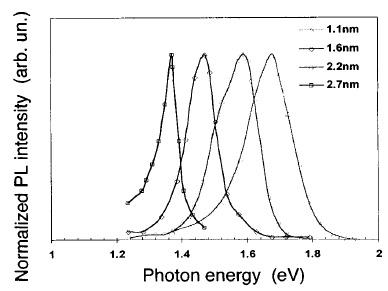
Figure 4. Photoluminescence (PL) from silicon quantum wells as a function of well thickness.
Low-temperature photoluminescence results from such silicon quantum wells are shown in Fig. 4. In accordance with simple confinement theory, the peak emission energy shifted upwards as the thickness of the final layer decreased, to values as high as 1.7 eV for layers of about 1 nm thickness.6 There was no evidence of oxide-mediated transitions that featured prominently in earlier work. The observed broadening could be well described by assuming a contribution to the signal from regions one atomic layer thicker and thinner than that primarily responsible for the observed response. Not shown in Fig. 4 is the increase in intensity by a factor of 30 as the dot size decreased from 2.7 nm to 1.1 nm, due to the strengthening of optical processes by confinement, as also expected.
3. Experimental approach
Our initial superlattice work involved deposition of alternate layers of dielectric followed by layers of amorphous silicon. These were furnace crystallized with laser treatment explored as a way of improving crystallographic quality. However, a slight modification to this approach suggested by Zacharias et al.9 which results in silicon quantum dots, has been the focus of subsequent work (Fig. 5).
As shown in Fig. 5, the deposition of each dielectric layer is followed by the deposition of a silicon-rich layer of the same dielectric, rather than pure silicon. On heating, silicon precipitates out of the silicon-rich layer in the form of silicon quantum dots, in what appears to be a 2D growth process, provided the layers are less than about 5 nm thick. This approach provides a way of controlling both the diameter of the dots and one of their spatial coordinates, as shown in Fig. 6.
Photoluminescence from such material shows the same general features as from quantum wells, with peak emission energy increasing from 1.3 eV to 1.7 eV as dot diameter decreased from 5 nm to 2 nm. Again, emission intensity strengthens as dot size decreases, offset by a counteracting tendency for the smallest dots.
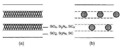
Figure 5. Method of forming silicon quantum dots in a dielectric matrix.9

Figure 6. (a) Si quantum dots in a SiO2 matrix formed using the approach of Fig. 5; (b) high-resolution image of a dot within material deposited onto a Si substrate.
4. Requirements for tandem cells
The key requirement for use in tandem cells is bandgap control, for which evidence is provided by the photoluminescence results. A bonus is the increased optical strength due to quantum confinement, reducing the required thickness of the quantum dot cells. Additionally, reasonable carrier transport properties are required, as represented by mobility-lifetime products greater than 10−9 cm2/V. Mechanisms to encourage directional transport within the cells are also required as provided by a pn junction in conventional cells. Control of the work function of the quantum dot material by doping or some other mechanism is therefore required. Finally, some mechanism of providing transport between the conduction and valence bands of adjacent cells is also required (Fig. 2). Tunnel junctions are generally used in good quality III-V cells to achieve this interconnection, while heavily doped junctions in amorphous material are sufficiently defective that they provide this connection via shunting. Progress towards demonstrating these requirements is described in the following sections.
5. Mobility and conductivity
Our group’s initial investigation of issues relevant to mobility assumed the quantum dots were uniform in size and were positioned on a regular cubic lattice. With some analytical simplification including an effective mass approximation, analytical solutions were derived similar to those for atomic lattices.10 By assuming a scattering time for electrons ten times smaller than the bulk silicon, idealized “Bloch” mobilities could be calculated as in Fig. 7.

Figure 7. Calculated Bloch mobilities for electrons in a cubic lattice of cubic silicon quantum dots (2 nm edges) as a function of lattice spacing for different silicon-based matrices.
These results suggested it might be difficult to obtain targeted mobilities above 1cm2/V.s using an oxide matrix, but that this might be easier with nitride and carbide matrices. However, it was relatively straightforward to extend the previous analysis to include random variations in both dot position away from the regular lattice and in dot size. It was found that the calculated mobility was not particularly sensitive to departures from the idealised spacing, with random variations up to about 30% tolerable without significant impact. However, the calculated mobility was extremely sensitive to dot size. Variations of less than 1% in diameter caused a significant decrease in mobility.
Essentially, for such low-mobility superlattices, 1% diameter variation pushed the energy of the confined state within extreme-sized dots outside the range of energies corresponding to the miniband in the idealized material (Fig. 2).
Since such tight control of dot size is not feasible experimentally, this suggests that Bloch transport will not be an important mechanism in our experimental material. Phonon-assisted hopping transport may be a more likely transport process. Experimental conductivity versus inverse temperature for nominally undoped quantum dots in oxide and nitride matrices are shown in Fig. 8. These confirm the expectation that transport will be easier in the nitride matrix, although these nitride results are preliminary.
6. Doping
The situation regarding doping of silicon quantum dots is unclear. Experimental work of Fujii and co-workers11 shows clear evidence for increasing free carrier concentration as phosphorus doping of the dots is increased, while theoretical work suggests that confinement increases dopant ionization energy to levels where ionization is unlikely at room temperature.12 For example, Fig. 9 shows calculated dopant ionization energies for the materials system of current interest calculated using the expressions derived by Lannoo et al.13

Figure 8. Lateral conductivity of silicon quantum dot material in oxide and nitride matrices vs. inverse temperature (nitride results are preliminary); corresponding activation energies are also shown.
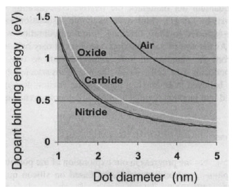
Figure 9. Calculated dopant ionization energy for a substitutional dopant centrally located in a silicon quantum dot embedded in the matrices indicated.
Embedding the dots in a high dielectric constant matrix tends to reduce the dopant ionization energy, although values are still too highly for significant ionization to be expected at room temperature. A high density of dots will increase the effective dielectric constant further, tending to further reduce this energy.
Our group is using ab-initio calculations to explore the properties of both conventional substitutional dopants as well as other strategies aimed at achieving the work function control provided by dopants in bulk material.
7. Excitons
The excitonic binding energy increases due to confinement in a similar way as the dopant binding energy.9 In a bulk semiconductor, even under non-equilibrium conditions, there is a natural dynamic equilibrium concentration of excitons nxde given by:14,l5
where np is the electron hole product and n* is a material constant depending on the electron, hole and excitonic densities of states and the excitonic binding energy Ebx (kBT is the thermal energy). The actual excitonic concentration, nx will deviate from this value to an extent determined by the association and disassociation rates that can be characterized by a binding lifetime ![]() B:
B:
For bulk silicon, ![]() B is in the picosecond range,12 and the excitonic concentration approaches its dynamic equilibrium value. Although excitons are present in reasonable densities in these materials even at room temperature, their equilibration with free carrier concentrations means they go largely unnoticed.
B is in the picosecond range,12 and the excitonic concentration approaches its dynamic equilibrium value. Although excitons are present in reasonable densities in these materials even at room temperature, their equilibration with free carrier concentrations means they go largely unnoticed.
In these quantum dot materials, the relative concentration of excitons will increase as given by Eq. (1). Moreover, excitonic association and disassociation rates might be expected to slow, resulting in non-equilibration with the electron-hole product. As the size of quantum dots decreases, it may be possible to observe a transition from the situation in bulk semiconductors to one more similar to organic semiconductor solar cells. There, the rate of disassociation of excitons into free carriers is believed to be so slow that specific exciton disassociation features are incorporated into junction regions to allow full photocurrent capture.
8. Conclusions
This chapter describes the progress in our exploration of the potential of a new type of quasi-amorphous semiconductor material based on silicon quantum dots in a dielectric matrix. The immediate motivation for this work is the potential for bandgap control that would allow the implementation of low-cost tandem solar cell structures based entirely on silicon.
Control of dot diameter and spacing has been demonstrated, as has bandgap control, as demonstrated by photoluminescence spectra. Current work is directed at demonstrating the required levels of carrier transport, as well as at understanding doping and the consequence of increased excitonic binding energy upon device design.
Our material could be useful for other semiconductor device applications where high carrier mobility is not required.
Acknowledgments
This work is supported by the Australian Research Council (ARC) under its Research Centres of Excellence Program and by Stanford University under the Global Climate and Energy Project (GECEP). The author gratefully acknowledges the contribution of other members of the ARC Photovoltaics Centre of Excellence, particularly G. Conibeer, D. König, E. C. Cho, D. Song, Y. Cho, T. Fangsuwannarak, Y. Huang, G. Scardera, E. Pink, S. Huang, W. C. Jiang, T. Trupke, R. Corkish, and T. Puzzer.
References
- M. Rogol, P. Choi, J. Conkling, A. Fotopolous, K. Peltzman, and S. Roberts, “Solar annual 2006: The gun has gone off,” Photon Consulting, July 2006.
- M.A. Green, Third Generation Photovoltaics, Berlin: Springer, 2003.
- M. A. Green, P. A. Basore, N. Chang, et al., “Crystalline silicon on glass (CSG) thin-film solar cell modules,” Solar Energy 77, 857 (2004).
- P. A. Basore, “CSG-2: Expanding the production of a new polycrystalline silicon PV technology,” 21st Eur. Photovoltaic Solar Energy Conf., Dresden, (2006).
- K. Yamagatu and T. Yonehara, “Bonding, splitting and thinning by porous Si in ELTRAN® SOI-epi waferTM,” MRS Spring Symp., San Francisco (2001).
- E.-C. Cho, P. Reece, M. A. Green, J. Xia, R. Corkish, and M. Gal, “Clear quantum confined luminescence from crystalline silicon/SiO2 single quantum wells,” Appl. Phys. Lett. 84, 2286 (2004).
- M. A. Green, J. Zhao, A. Wang, P. J. Reece, and M. Gal, “Efficient silicon light emitting diodes,” Nature 412, 805 (2001).
- T. Trupke, J. Zhao, A. Wang, R. Corkish, and M. A. Green, “Very efficient light emission from bulk crystalline silicon,” Appl. Phys. Lett. 82, 2996 (2003).
- M. Zacharias, J. Heitmann, R. Scholz, U. Kahler, M. Schmidt, and J. Blaesing, “Size-controlled highly luminescent silicon nanocrystals: A Si/SiO2 superlattice approach,” Appl. Phys. Lett. 80, 661 (2002).
- C.-W. Jiang and M. A. Green, “Silicon quantum dot superlattices: Modelling of energy bands, densities of states and mobilities for silicon tandem solar cell applications,” J. Appl. Phys. 99, 114902 (2006).
- M. Fujii, Y. Yamaguchi, Y. Takase, K. Ninomiya, and S. Hayashi, “Photoluminescence from impurity co-doped and compensated Si nanocrystals,” Appl. Phys. Lett. 87, 211919 (2005).
- Z. Zhou, M. L. Steigenwald, R. A. Friesner, L. Brus, and M. S. Hybertsen, “Structural and chemical trends in doped silicon nanocrystals: First-principles calculations,” Phys. Rev. B 71, 245308 (2005).
- M. Lannoo, C. Delerue and G. Allan, “Screening in semiconductor nanocrystallites and its consequences for porous silicon,” Phys. Rev. Lett. 74, 3415 (1995).
- M. A. Green, Silicon Solar Cells: Advanced Principles and Practice, Sydney, Australia: University of New South Wales, 1995.
- R. Corkish, D. S.-P. Chan, and M. A. Green, “Excitons in silicon diodes and solar cells – A three particle theory,” J. Appl. Phys. 79, 195 (1996).