
Formation of Three-Dimensional SiGe Quantum Dot Crystals
Laboratory for Micro- and Nanotechnology
Paul Scherrer Institute, Villigen, Switzerland
Inst. für Halbleiter und Festkörperphysik
Johannes Kepler University Linz, A-4040 Linz, Austria
1. Introduction
Silicon based quantum dot materials are gaining attention due their potential for ultimate CMOS devices1 or for beyond-CMOS device architectures.2-4 Germanium dots incorporated in Si are particularly promising because their fabrication can take advantage of the well-developed Si technology. The long spin coherence times in Si5-7 represent another advantage of this material system, opening possible routes towards spintronics and quantum computation. The embedding of individually addressable Ge quantum dots into Si device technology might be crucial to open new paths for the fabrication of high speed electronics. Self-assembled Ge dots, which nucleate randomly on the surface and have typically a rather broad distribution in their sizes, have been studied intensively. Across a large window in deposition temperature a bimodal distribution of Ge islands is found, with small Ge huts coexisting with large Ge dome clusters.8 However, many proposed devices, like the dot-FET9 or dot arrays for qubit information technology,2-4 require a uniform size distribution. Moreover, the addressing of individual dots will require the positioning of dots on predefined spots. In most approaches, a combination of pre-patterned substrates and self-assembled deposition was employed to achieve lateral ordering.10,11 In the Si/Ge material system, patterns written by e-beam lithography and two-dimensional (2D) patterns fabricated by optical interference lithography have been used to achieve ordering of dome clusters.12,13 Using CVD processes, Ge dots have also been selectively grown in oxide patterns.14,15 However, these Ge islands were rather large and intermixed strongly with Si due to growth temperatures exceeding 600 °C.
In this chapter we present the lateral and 3D ordering of small Ge hut clusters on pre-patterned Si (100) surfaces. The pre-pattern was fabricated by X-ray interference lithography (XIL) using a dedicated beam line at the Swiss Light Source (SLS). XIL offers precise control over the periodicity of the pattern as well as patterns with periodicities in the sub-50 nm regime. The capability to expose an area of 2×2 mm with a single shot, makes this technology a powerful alternative to e-beam lithography to fabricate structures in nanotechnology.
2. Fabrication and discussion
The process to fabricate ordered 2D and 3D arrays of Ge quantum dots starts with the formation of the pre-pattern on the (100) Si substrate. Silicon substrates were coated with PMMA resist and transferred into the vacuum chamber of the XIL beam line at the SLS.16 Typically, areas of 0.7×0.7 mm were patterned in a single exposure. Multiple-beam diffraction was employed to achieve the exposure of 2D patterns. The gratings used for multiple-beam diffraction were fabricated using e-beam lithography from Si substrates coated with a SiNx and a Cr film. After transferring the gratings into the Cr film, the Si underneath was removed, leaving the Cr gratings on free-standing SiNx membranes. In our experiments, XIL was used to write patterns of either 90×100 nm or 250×250 nm into the PMMA resist. The pattern was transferred into the Si substrate by reactive ion etching (RIE). The depth of the pattern was restricted to 8–20 nm. After removal of the PMMA resist and cleaning of the patterned Si substrates, they were transferred into the solid source Si/Ge molecular beam epitaxy (MBE) system. The substrates were heated to 550 °C to remove the hydrogen from the surface and subsequently a 50 nm Si buffer layer was deposited at low temperatures. Note, that no high temperature anneal for in-situ cleaning of the Si substrate before the MBE process was employed. This requires special care during the wet chemical cleaning process to avoid build-up of contamination on the substrate. For 2D arrays of quantum dots, a single Ge island layer was deposited next; whereas for 3D quantum dot crystals, a multiple layer sequence of Ge dot layers and 10 nm Si spacer layers was grown.
The structures were analyzed using atomic force microscopy (AFM), transmission electron microscopy (TEM) and x-ray diffractometry. Figure 1 shows AFM images at different stages of the deposition process. In Fig. 1(a), a 2D hole array has been generated with a periodicity of 90×100 nm in the Si substrate using XIL exposure and subsequent RIE to transfer the pattern into the substrate. An exposure dose of 55 mJ measured at the location of the diffractive mask was used to expose the PMMA resist during XIL. After developing the resist, the checkerboard-like pattern consists of square holes with a depth of 8 nm and a periodicity of 90×100 nm in the x-y plane. The depressions appear dark in the AFM images of Fig. 1(a), (b), (d) and (e). The size of the holes is such, that they are still separated from each other, i.e. barely touching each other at their corners. Figure 1(b) shows this grating after the deposition of a 50 nm buffer layer. The holes shrunk in size and depth during the deposition of the buffer layer. The diameter is around 20 nm and the depth is about 4 nm. The Si surface around the holes is smooth. Figure 1(c), shows the final topography of the sample measured by AFM after the deposition of 7 monolayers of Ge. This thickness is above the critical thickness for Ge film deposition on Si, thus Ge islands have formed. The dots appear bright in the image of Fig. 1(c). A very regular array of Ge dots is formed with a density of 1.1×1010 cm-2. The dots nucleate at the hole sites prepared by XIL and subsequent RIE. No islands are found on Si surfaces surrounding the holes. An island has nucleated in every hole, with no missing islands found within the inspected area. The islands have an almost square base and they are (105) faceted from bottom to the top, thus they belong into the category of Ge hut clusters.8 Note that no elongated hut clusters with strongly rectangular bases have formed.
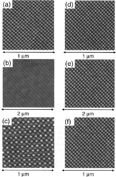
Figure 1. Formation of ordered arrays of Ge quantum dots described by AFM surface scans: (a) pre-patterned Si; (b) after the deposition of a 20 nm Si buffer, (c) ordered array of Ge quantum dots; (e)-(f) same experiment but using a higher exposure dose leading to twice the dot density.
Figures 1(d–f) show the same sequence for a sample that had been exposed with a higher dose during XIL, namely 75 mJ (measured at the mask). The higher dose leads to larger holes in the resist after the PMMA development. Again RIE was used to transfer the pattern into the Si substrate. Figure 1(d) shows that in this case the holes are touching each other. As a result, the substrate actually contains of an array of small Si pillars with a square base, which are bright in the AFM image of Fig. 1(d). The overgrowth of this pattern with a 50 nm thick Si buffer layer leads to the formation of a cross grating on the Si surface. In other words, the substrates has a periodic array of holes, however, these holes are linked to each other by grooves. Due to these grooves, the slight asymmetry of the 90×100 nm pattern in the x-y plane can be clearly seen in the AFM image of Fig. 1(e). The groves are aligned along the <110> directions of the Si (100) substrate. This pattern has also been overgrown by 7 monolayers of Ge using MBE. Again, a regular array of dots is formed, as shown in the AFM image of Fig. 1(f). Surprisingly, the islands do not nucleate in the holes, which are the deepest suppressions in the substrate, but within the grooves connecting the holes. Consequently, the dots have twice the density compared to those nucleating on the pattern shown in Fig. 1(a).
The dots have an elongated shape induced by the grooves. Notably, this is not the shape of elongated hut clusters,17 which have a rectangular base along <001> directions. Here the grooves are along the <110> directions and accordingly the dots are stretched into this direction, leading to a rhombus-shaped base of the islands. Some islands appear to be formed from two adjacent nuclei. Most likely the sidewalls of the groves aligned along the <110> directions are (111) facets, since those are the slowest growing planes in Si. The fact that the islands nucleate in the grooves may indicate that corners of two adjacent (111) facets are preferred nucleation sites for Ge islands.
In order to fabricate 3D quantum dot crystals, the pre-patterned substrates have been overgrown by sequences of Ge and Si layers. Here, we used the process to fabricate the template Si substrate and the first island layer as described in Fig. 1 (a-c). Figure 2 shows a cross-sectional TEM image (Z-contrast) of such a sample with 10 periods. The first period consisted of the 50 nm Si buffer layer and the first Ge dot layer (7 monolayers of Ge), whereas the subsequently grown nine periods contain 10 nm Si layers and 5 monolayer-thick Ge layers. The TEM micrograph clearly shows that the first Ge layer leads to the nucleation of Ge islands within the holes of the substrate. Thus this fust Ge islands have an increased aspect ratio compared to conventional (105) faceted Ge huts. After the deposition of the first 10 nm Si spacer, the surface of the sample appears flat: the topography due to the pre-patterning and the island nucleation has vanished. However, the Ge islands are relaxed towards their apex, inducing tensile strain into the part of the Si layer covering the dot. Accordingly, the 10 nm Si spacer contains an undulating strain field reflecting the periodicity of the underlying Ge island layer. The next layer of Ge is affected by this strain field and Ge islands nucleate in those areas of the Si spacer layers that are under tensile strain, since the in-plane lattice constant is larger in these areas and hence better matched to the Ge lattice constant. This effect of vertical stacking of self-assembled Ge islands is well understood.18 Here we make use of this effect to build up the 3D quantum dot crystal, since the lateral orderillg of the Ge dots in the first dot layer will be transferred in the subsequently grown Ge layers by this self assembly.
The TEM micrograph in Fig. 2 nicely shows the stacking of the Ge islands. Neither Z-contrast nor conventional TEM micrographs reveal interface contamination or defects of the crystalline structure. In particular, the interface between the pre-patterned substrate and the first buffer layer is not visible.
The structural properties were investigated by x-ray diffractometry to gauge the crystalline perfection of the quantum dot crystal. Reciprocal space maps were recorded with a Seifert XRD 3003. The primary beam was prepared using a Göbel mirror. a single Ge (220) channel cut crystal, and a 1 mm slit. On the secondary side, a position sensitive detector (PSD) was used. Two maps in the [110] azimuth were recorded, the symmetrical (004) and the asymmetrical (224), as shown in Fig. 3.

Figure 2. Z-contrast TEM image a ten-period 3D quantum dot crystal with a lateral periodicity of 90×100 nm and a vertical periodicity of 11 nm.
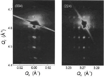
Figure 3. Reciprocal space maps of the Si/Ge quantum dot crystal taken at the symmetrical (004 – left) and the asymmetrical (224 – right) reflex.
From these maps, the lateral and vertical periods are obtained as 90.7 and 11.4 nm, respectively. By rotating the sample by 90° to change the azimuth, the second lateral periodicity of 100.2 nm is found. This is in good agreement with the nominal values. From the (224) map, one can see that the envelope of the satellites is shifted to small Qx values, which is an indication of elastic relaxation in the Ge islands. Detailed analysis of this data, to gather insight into the Ge concentration of the islands, will be a subject of future study.
From the AFM and TEM data it can be found that the dots in the 3D dot crystal have a diameter of 20±5 nm, thus Ge dots exhibit a remarkably narrow size distribution and close to perfect ordering.
Figure 4 shows photoluminescence (PL) spectra obtained from structures containing a single Ge layer, two Ge dot layers and finally ten dot layers forming a 3D dot crystal. The single Ge layers of 3, 5.4 and 7 monolayer thicknesses were capped with 100 nm of Si, the double layer had a 10 nm cap layer and the crystal was uncapped, thus the topmost dot layer is exposed to air and most likely does not contribute to the PL spectrum. In order to interpret the PL spectra correctly, one has to consider that the radiative transitions in this Si/Ge system are indirect in both real and reciprocal space. Thus the complexity of the confinement situation for electrons and holes in these structures has to be considered. Isosurfaces of the wavefunctions around a SiGe quantum dot have been calculated by the nextnano3 simulation package.19 This simulation package provides quantitative information on quantized bound state energies for arbitrarily shaped 3D nanostructures, using a single-band k·p Hamiltonian. Elasticity theory is used to globally minimize the strain and local strain fields are incorporated into the band structure using deformation potential theory. Using the calculated energy levels and their dependence on the Ge concentration in the QD, the Ge content of the QDs can be estimated. Assuming a Si0.5Ge0.5 (Si0.3Ge0.7) dot and a QD shape as observed for the first QD layer (see Fig. 2), a calculated Δz1–HH transition energy of 770 (580) meV and a Δxy-HH1, transition energy of 810 (650) meV are obtained. Depending on the strain fields and on the composition gradients within the islands and considering the fact that at the large excitation densities used in these PL experiments several electron states around the QDs are likely to be occupied, a rather broad PL, signal can be expected. This is true despite the narrow size distribution of the dots because many electron-hole transitions are optically allowed and the electrons are confined at different potential minima surrounding the dot having slightly different energies.
Furthermore, the stacking of Ge dots in the double layer and in the ten-period crystal will enhance the strain field between the dots and consequently increase the confinement energy for electrons.20 In a stack of dots this strain field is strongest in the centre of the stack and gets weaker towards the bottom and top Ge dot layers. This change in the strain field in stacked dots leads to different confining potentials for the electrons20,21 and, in turn, to a broadening of the PL line of stacked Ge dots. Thus, even if the Ge dots were all perfectly identical, a broadened PL line would be expected. These considerations should be kept in mind when interpreting the PL data shown in Fig. 4. All spectra are obtained from the pre-patterned areas of the sample. The dominant sharp line in the spectra at 1090 meV is the phonon-assisted replica of the Si substrate (Si-TO). The spectrum at the bottom of Fig. 4 is obtained for a three monolayer Ge layer embedded in Si, below the critical thickness for island formation, which is confirmed by the PL data showing a double peak below the Si-TO line typical for Ge wetting layer luminescence (marked WL in Fig. 4).21 The deep broad peak (labelled D) around 730 meV is assigned to defects in the Si substrate. since this peak is observed for the as-received Si substrates. It is present in all single layer dot samples as well as in the double layer structure. It is not present in the quantum dot crystal, which has been deposited on a different Si substrate of higher quality. Increasing the Ge layer thickness to 5.4 monolayers leads to island formation. In the PL spectrum, the wetting layer PL is shifted to lower energies due to the increased thickness and a new peak appears between the wetting layer PL and the defect band. As indicated in Fig. 4, this peak is assigned to the Ge dots. The wetting layer PL is shifted to a lower energy compared to literature data,21 which might be attributed to Ge agglomeration in the areas between the dots. A further increase of the Ge layer thickness to 7 monolayers shifts the wetting layer PL only slightly and the dot PL to lower energies (784 meV), overlapping with the substrate defect band at 730 meV. Thus, experimentally, for a seven-monolayer single dot layer, the QD PL peak is observed around 784 meV. This value is very close to the calculated Δxy−HH1 transition energy for a Si0.5Ge0.5 QD. Thus, from this comparison, a Ge concentration close to 50% is estimated. In a next step a second island layer (5 monolayers of Ge) has been added, separated by an 8 nm wide spacer layer from the first island layer (7 monolayers of Ge). The PL spectrum of the sample does not show resolved wetting layer luminescence, consistent with literature data,21 where this effect has been explained by tunnel processes between closely spaced island layers. The PL line at 815 meV is attributed to the Ge hut clusters in the upper Ge layer. The peak is asymmetric with a tail towards lower energies, due to the overlap with the bigger Ge dots in the lower layer and the substrate defect line. Finally, the top spectrum in Fig. 4 shows the PL data of the ten-period Ge quantum dot crystal. The spectrum reveals a strong line centered at 746 meV. The shift in energy is explained by the increased confinement energy for electrons in stacked dots,20 as well as by the vertical coupling of the dots shifting the quantized hole energy level. The inset in Fig. 4 shows the high-temperature PL of a ten-period Ge dot crystal. The luminescence of the Ge dots in persists up to room temperature, indicating a low defect density in the samples.
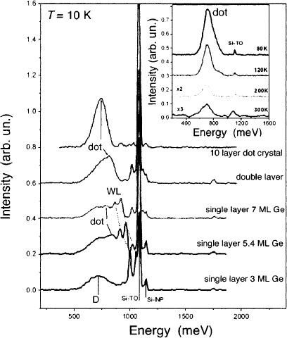
Figure 4. Comparison of low temperature (T = 10 K) photoluminescence of Si/Ge quantum dot crystals containing 1, 2 and 10 periods of dots. The inset shows high temperature photoluminescence (T = 80–300K) of a three-dimensional Ge quantum dot crystal.
3. Conclusions
We have successfully fabricated 2D and 3D Si/Ge quantum dot crystals consisting of closely packed Ge islands. X-ray interference lithography (XIL) was employed to write arrays of 2D periods into PMMA resist and transfer the patterns into Si (100) substrates, which were used as templates for the deposition of ordered arrays of islands. Changing the x-ray exposure conditions and thereby the shape of the template makes it possible to control the shape and density of the Ge islands. Using the method of templated self-organization in combination with vertical stacking of Ge islands, 3D dot crystals were formed. Atomic force microscopy, x-ray diffraction and TEM analysis reveal the high perfection of those dot crystals. Photoluminescence measurements indicate a low defect density in the quantum dot structures.
Our results on the fabrication and properties of 2D and 3D Ge quantum dot crystals may open new routes towards the realization of nanoelectronic and spintronic devices as well as for quantum computing.
References
- O. G. Schmidt, A. Rastelli, G. S. Kar, et al., “Novel nanostructure architectures,” Physica E 25, 280 (2004).
- D. Loss and D. P. DiVincenzo, “Quantum computation with quantum dots,” Phys. Rev A 57, 120 (1998).
- B. E. Kane, “A silicon-based nuclear spin computer,” Nature 393, 133 (1998).
- M. Friesen, P. Rugheimer, D. E. Savage, et al., “Practical design and simulation of silicon-based quantum-dot qubits,” Phys. Rev. B 67, 121301 (2003).
- G. Feher and E. A. Gere, “Electron spin resonance experiments on donors in silicon. II. Electron spin relaxation effects,” Phys. Rev. 114, 1245 (1959).
- C. Tahan, M. Friesen, and R. Joynt, “Decoherence of electron spin qubits in Si-based quantum computers,” Phys. Rev. B 66, 035314 (2002).
- J. P. Gordon and K. D. Bowers, “Microwave spin echoes from donor electrons in silicon,” Phys. Rev. Lett. 1, 368 (1958).
- A. Rastelli and H. von Känel, “Surface evolution of faceted islands,” Surf Sci. 515, L493 (2002).
- O. G. Schmidt and K. Eberl, “Self-assembled Ge/Si dots for faster field-effect transistors,” IEEE Trans. Electron Dev. 48, 1175 (2001).
- E. S. Kim, N. Usami, and Y. Shiraki, “Control of Ge dots in dimension and position by selective epitaxial growth and their optical properties,” Appl. Phys. Lett. 72, 1617 (1998).
- D. S. L. Mui, D. Leonard, L. A. Coldren, and P. M. Petroff, “Surface migration induced self-aligned InAs islands grown by molecular beam epitaxy,” Appl. Phys. Lett. 66, 1620 (1995).
- O. G. Schmidt, N. Y. Jin-Phillipp, C. Lange, et al., “Long-range ordered lines of self-assembled Ge islands on a flat Si (001) surface,” Appl. Phys. Lett. 77, 4139 (2000)
- Z. Zhong, A. Halilovic, T. Fromherz, F. Schäffler, and G. Bauer, “Two-dimensional periodic positioning of self-assembled Ge islands on prepatterned Si(001) substrates,” Appl. Phys. Lett. 82, 4779 (2003).
- T. I. Kamins and R. S. Williams, “Lithographic positioning of self-assembled Ge islands on Si(001),” Appl. Phys. Lett. 71, 1201 (1997).
- L. Vescan and T. Stoica, “Luminescence of laterally ordered Ge islands along <100> directions,” J. Appl. Phys. 91, 10119 (2002).
- H. H. Solak, C. David, J. Gobrecht, et al., “Sub-50 nm period patterns with EUV interference lithography,” Microelectronic Eng. 67, 56 (2003).
- Y.-W. Mo, D. E. Savage, B. S. Swartzentruber, and M. G. Lagally, “Kinetic pathway in Stranski-Krastanov growth of Ge on Si(001),” Phys. Rev. Lett. 65 1020 (1990).
- F. Liu, A. H. Li, and M. G. Lagally, “Self-assembly of two-dimensional islands via strain-mediated coarsening,” Phys. Rev. Lett. 87, 126103 (2001).
- J. A. Majewski, S. Birner, A. Trellakis, M. Sabathil, and P. Vogl, “Advances in the theory of electronic structure of semiconductors,” Phys. stat. sol. C 1, 2003 (2004).
- O. G. Schmidt, K. Eberl, and Y. Rau, “Strain and band-edge alignment in single and multiple layers of self-assembled Ge/Si and GeSi/Si islands,” Phys. Rev. B 62, 16715 (2000).
- O.G. Schmidt and K. Eberl, “Multiple layers of self-assembled Ge/Si islands: Photoluminescence, strain fields, material interdiffusion and island formation,” Phys. Rev. B 61, 13721 (2000).