
Robust Metallic Interconnects for Flexible
Electronics and Bioelectronics
Division of Engineering, Brown University, Providence, RI 02912, U.S.A.
1. Introduction
Integrated interconnects for electronic applications have traditionally been restricted to planar rigid substrates that place negligible mechanical constraints on their performance. However, the continued interest in flexible electronic applications and convergence of biomedical implants with conventional electronics, necessitates the development of robust flexible interconnect schemes. Flexible electronics will encompass many applications, such as wearable electronics, large-area sensor arrays, bendable and conformal solar cell arrays, flexible displays, as well as flexible (and possibly stretchable) implantable biosensors.
In the case of next generation flexible displays, flexible interconnects are seen as one of the key enabling technologies that will bring the concept of rollable and bendable screens to fruition. Flexible display applications, which broadly include bendable, conformable and rollable displays,1 will require flexible substrates, electronic components, optical layers as well as robust circuitry for functionality and reliable performance. Figure 1 shows a concept flexible display that allows for full rollability, similar to a conventional newspaper.

Figure 1. A concept flexible display device that can be rolled out to show an image and rolled back into a tube to be stowed away.
Flexible display devices will make it possible to roll out a screen for viewing images and roll it back into small form factors, delivering images larger than the area of the display itself. Flexible display applications have been demonstrated with liquid crystals,2 electrophoretic inks,3 organic light emitting diodes,4 microelectro-mechanical systems, and hollow fiber elements.5 Regardless of the display technology incorporated into the device, an underlying commonality for this wide array of technologies is an interconnect scheme that maintains the electrical integrity of the interconnect material when the devices are bent, rolled, or flexed.6
Some possible candidates for flexible interconnect materials include conducting polymers, printed carbon pastes, carbon nanotube dispersions, and thin metal films. Although all the aforementioned candidates have their merits and demerits, thin metal film interconnects appear most suitable for flexible display circuitry because of their inherently high conductivity. The conductivity of conducting organic materials is still orders of magnitudes less than metals, whereas other technologies, like carbon nanotube dispersions, may prove difficult to integrate into existing electronic fabrication processes. Compared to all the other materials, thin metal films demonstrate excellent electro-mechanical performance, even when subjected to mechanical strain.7,8,9
Flexible interconnects are also crucial for biomedical application that require interconnectivity between implantable microchips, various sensors and electronic devices. At a minimum, the flexible electrodes are required to have low electrical resistance, provide mechanical flexibility with no appreciable change in conductivity and, in cases that involve implantation into biological materials, be nontoxic and biocompatible. Interconnects for these hybrid electro-biological systems should also be smooth, robust, lightweight and properly insulated.10
In this chapter, we describe a robust metallization scheme ideal for electrodes and interconnects suitable for flexible display applications11,12 and possibly for bioelectronic applications as well. The metallization scheme consists of a multilayered structure of thin granular metal films deposited on a flexible substrate. The multilayered stack includes a granular discontinuous ductile indium layer that shows minimal resistance changes even when subjected to large mechanical strains and repeated low-strain fatigue loading. To fully demonstrate the potential of the interconnect scheme, we fabricated a simple flexible prototype display by incorporating patterned electrodes made by a standard photolithographic process.
2. Flexible interconnect materials and processing
Thin-metal film interconnects, containing chromium, indium and gold, were deposited onto dog bone-shaped polyethylene terephthalate (PET) and highly formable film (HFF) substrates, carefully prepared to minimize edge defects which could potentially lead to a localization of the applied strain and lead to a premature rupture in the films. Figure 2 shows a photograph of the testing system and a scanning electron micrograph (SEM) of a Cr/In film. The HFF substrates exhibit thermal properties similar to conventional PET, however, they can be stretched much more easily and their formability can be improved by heating. Such HFF substrates are particularly suitable for conformal display application, because they are engineered for bending and embossing (even 90° corners), which may not be achievable with standard PET. For both substrates, two types of films were fabricated: films deposited on the entire surface of a dog-bone shaped substrates and films patterned as thin lines using a shadow mask in the gauge length of the dog-bone shaped substrate, as shown in Fig. 2(a). The samples were loaded in a Minimat Miniature Tensile tester system, which can provide uniaxial tensile loading. The multilayered metal interconnects deposited on the polymer substrates consisted of a 5 nm chromium (Cr) adhesion layer, followed by a 50 nm granular indium (In) film and in some cases an additional 10 nm thick gold layer to increase conductivity and encapsulate the indium layer. All the metal films were deposited by electron-beam evaporation at room temperature at a deposition rate of ~0.1 nm/sec. The indium islands cover 75% of the total film area, with average diameter of 500 nm, as shown in Figure 2(b). The electro-mechanical performance of different multilayer structures based on thin films of chromium, indium and gold deposited on PET and HFF substrates was investigated.
3. Uniaxial tensile strain test and results
The electro-mechanical performance of thin-metal films patterned as interconnects on polymer substrates was evaluated by monitoring the electrical resistance as a uniaxial tensile force was applied to both ends of the film. Figure 3 shows an illustration of the thin-metal-coated polymer film before and after a uniaxial tensile strain was applied. As depicted in the illustration, cracks were observed to form and propagate in the stiffer underlying chromium adhesion layer. The presence of In islands bridging the cracks, evident in the SEM micrographs of Fig. 4, maintains the electrical integrity of the metal line. The top Au layer can be used to further improve the electrical conductivity of the film.
Figure 2. (a) Photograph of a Cr/In (5/50 nm) interconnect sample loaded in tensile strain. (b) SEM micrograph showing the granular indium layer deposited on a Cr-coated PET substrate.
Although the electrical resistance of the interconnects was observed to increase with increasing strain, there was no abrupt change or loss of electrical integrity over a wide range of strain values for all samples tested. Interconnects fabricated on PET substrates were observed to deform uniformly over the entire gauge-length of the dog bone-shaped sample, and remained conducting until the PET substrate itself ruptured at strain ε = 38%. In the HFF samples, on the other hand, the deformation was concentrated in the mid-section of the gauge-length, thus causing a localization of the stress in the interconnect. Notwithstanding this peculiar deformation characteristic of the HFF substrate, the thin-metal film interconnects were observed to be electrically conductive even after applying a strain of >100% to the HFF sample. Figure 4 shows the stress-strain curves together with the normalized change in resistance ΔR/R0 ≡ (R−R0)/R0, for Cr/In/Au interconnects deposited on the two different substrates.11,12
The change in resistance of the interconnects deposited on a PET substrates, was observed to be <100% at an applied external strain of 38%. The resistance increase is a result of crack formation and geometry changes in the films. Cracks form perpendicular to the loading direction and increase in size and density with increasing applied strain for continuous films. The island structure of the indium layer however, deforms continuously through an elastic mechanism in which they extend across the cracks formed in the underlying chromium layer, as shown in the SEM insets of Fig. 4. The normalized change in resistance of the Cr/In/Au film showed a steady increase with no catastrophic failures for both substrates, although the recorded values were two orders of magnitude higher with the HFF substrate. The observed geometric deformation in the HFF substrate is dominated by a necking phenomenon, resulting in local strains of more than 300% and relatively bigger change of the resistance. It should be noted that the strains applied in Fig. 4 vastly exceed any anticipated deformation required of flexible interconnects.

Figure 3. Schematic illustration of thin granular film structure (a) before and (b) after a tensile force is applied at both ends of the sample.

Figure 4. Stress-strain curve with change in resistance for interconnects on a PET (top) and HFF (bottom) substrates; insets show SEM micrographs of the bridging mechanism after applied tensile strain.
4. Cyclic fatigue loading
Flexible electronic applications designed to undergo continuous flexing, rolling and bending during fabrication or while in use, must also be robust enough under repeated low-strain fatigue conditions. Samples of the indium island-containing films were tested on a custom-built fatigue tensile-tester for 10,000 bend cycles. In this test, the thin films deposited on both PET and HFF substrates were repeatedly rolled and unraveled around a half-inch diameter cylindrical mandrel (resulting in a strain ε ~ 2%). The fatigue test system as well as the results from this test is presented in Fig. 5.
The results clearly show that there is negligible change in the resistance of the interconnects due to fatigue loading. The very small apparent fluctuations in the measured resistance can be attributed to the resolution and inherent vibrations present in the test system.
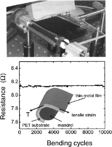
Figure 5. Photograph of cyclic fatigue testing apparatus (top) and the measured two-point resistance (bottom) of a Cr/In/Au film deposited on a PET substrate after 10,000 cycles showing less than a 0.01% change in electrical resistance.12
5. Prototype flexible display
We have fabricated a simple, proof-of-concept single-pixel flexible display on a 5×5 cm PET substrate. A 5/50/10 nm Cr/In/Au interdigitated electrode was fabricated by conventional lithography, e-beam metal evaporation, and lift-off, as shown in Fig. 6. A conventional polymer dispersed liquid crystal (PDLC) film deposited on top of the flexible electrode resulted in a fully functional and bendable display. The PDLC film was made on the patterned electrodes and using a polymer-induced phase separation to obtain micron-sized liquid crystals trapped within an extended polymer matrix. Figures 7(a) and (b) shows photographs of the flat device in both a power-on and power-off state, after being bent to ~1 cm radius of curvature for 100 times. In the “on” state (a), the film is transparent, showing the “BROWN” image printed on the back; while in the “off” state the film is opaque. Figure 7(c) shows the “on” state of the bent device bent to ~1 cm radius of curvature, again displaying the “BROWN” image. There is no fundamental obstacle to scaling this type of display to many pixels via lithographic interconnection of small PDLC pixels with our flexible metal lines.
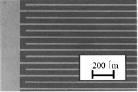
Figure 6. An optical micrograph of interdigitated electrodes fabricated on a PET substrate showing sharp features.
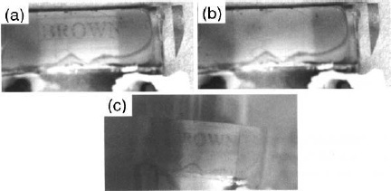
Figure 7. (a) Transparent “on” state of a flat device. (b) Opaque “off” state of a flat device. (c) Transparent “on” state of the device bent to ~1 cm radius of curvature.
7. Potential biomedical applications
Beside flexible display application, flexible interconnects hold promise for biomedical applications. Metal film interconnects have in recent years been incorporated into devices for interfacing with parts of the central or peripheral nervous system for neuronal disorders,10 have enabled electronic stimulation of retinal neurons,13 and have been integrated into various neural biohybrid interfaces.14
For instance, the flat interface nerve electrode (FINE) chip15 can functionally stimulate a selected peripheral nerve, while reshaping the nerve into a configuration of axons closer to the stimulating contacts by increasing the nerve surface area. During this process, an elastomer clip will deform both by opening to go over the fiber and by bending in a slight arc as it is closed to put pressure on the bundle. One challenge is to interconnect the various functional blocks and the electrodes on the elastomer clip. At the same time, the interconnect must withstand the complex body environment.
As an initial test, our Cr/In films were dipped into a physiological saline solution for a week. After that, the resistance was measured and the samples were observed under SEM, with no change found. After a week in saline, Cr/In (5/500 nm) films deposited on PET were tested with the Minimat tester system. The resistance slightly changed from 2 Ω/square to 3.4 Ω/square at ε = 35% strain, which is sufficient for most biomedical applications. Although these preliminary results are promising, further research is needed. Thus far, we have mainly focused our research on PET and HFF substrates suitable for displays, while for biomedical application elastomer (silicone) substrates are widely used. Compared to PET, elastomers have rather different mechanical properties, with a much smaller Young’s modulus and a much rougher surface, making film adhesion problematic. Further, the biocompatibility of In has not been fully investigated.
8. Conclusions
The inclusion of a granular layer of indium islands enhances the ultimate stretchability and reliability of thin-film interconnects and electrodes compatible with compliant display substrates. We have demonstrated the patternability of this robust and flexible electrode scheme on PET by using a standard photolithography process. Additionally, we have shown that there is no degradation in performance of the electrode or the display when repeatedly bent around a ~1 cm radius of curvature.
Our preliminary results have shown the compatibility of Cr/In films and physiological saline solution. The benefits of the stretchable interconnects present a great opportunity for bioelectronic applications that require patternable interconnect materials to connect electronic devices to biological materials.
Acknowledgements
The work at Brown University was supported by the MRSEC/NSF (DMR-0079964) and by NSF ECS-0223943 and NSF CCF-0403958. The authors acknowledge the use of the Microelectronics Central Facility at Brown, supported by the NSF MRSEC (DMR-0079964).
References
- G. P. Crawford, ed., Flexible Flat Panel Displays, New York: Wiley, 2005.
- B. S. Kim, M. Hong, Y. U. Lee, et al., “Developments of transmissive a-Si TFT-LCD using low temperature processes on plastic substrate,” Soc. Inform. Display Digest 35, 19 (2004).
- T. Whitesides, M. Walls, R. Paolini, et al., “Towards video-rate micro-encapsulated dual-particle electrophoretic displays,” Soc. Inform. Display Digest 35, 133 (2004).
- J. Innocenzo and E. I. Dupont, “Roll to roll PLED process development,” Soc. Inform. Display Digest 33, 884 (2002).
- M. Nakata, M. Sato, Y. Matsuo, S. Maeda, and S. Hayashi, “Hollow fibers containing various display elements: A novel structure for electronic paper,” J. Soc. Inform. Display 14, 729 (2006).
- S. J. Gorkhali, D. R. Cairns, and G. P. Crawford, “Reliability of transparent conducting substrates for rollable displays: A cyclic loading investigation,” J. Soc. Inform. Display 12, 45 (2004).
- T. Li, Z. Huang, Z. Suo, S. P. Lacour, and S. Wagner, “Stretchability of thin metal films on elastomer substrates”, Appl. Phys. Lett. 85, 3435 (2004).
- S. P. Lacour, J. Jones, S. Wagner, T. Li, and Z. Suo, “Stretchable interconnects for elastic electronic surfaces,” Proc. IEEE 93, 1459 (2005).
- D. S. Gray, J. Tien, and C. S. Chen, “High-conductivity elastomeric electronics,” Adv. Mater. 16, 393 (2004).
- T. Stieglitz, H. Beutel, M. Schuettler, and J.-U. Meyer, “Micromachined, polyimide-based devices for flexible neural interfaces”, Biomed. Microdev. 2, 283 (2000).
- D. P. Wang, F. Y. Biga, A. Zaslavsky, and G. P. Crawford, “Electrical resistance of island-containing thin metal interconnects on polymer substrates under high strain,” J. Appl. Phys. 98, 086107 (2005).
- D. P. Wang, F. Y. Biga, A. Zaslavsky, and G. P. Crawford, “Robust-stretchable interconnects for flexible display applications”, to appear in Soc. Inform. Display Digest 37 (2006).
- E. T. Kim, J. M. Seo, J. A. Zhou, H. Jung, and S. J. Kim, “A retinal implant technology based on flexible polymer electrode and optical/electrical stimulation,” IEEE Intern. Workshop BioCAS (2004), S1.8-12.
- T. Stieglitz, H. H. Ruf, M. Gross, M. Schuettler, and J.-U. Meyer, “A biohybrid system to interface peripheral nerves after traumatic lesions: Design of a high channel sieve electrode,” Biosensors Bioelectronics 17, 685 (2002).
- D. J. Tyler and D. M. Durand, “Functionally selective peripheral nerve stimulation with a flat interface nerve electrode,” IEEE Trans. Neural Syst. Rehab. Eng. 10, 294 (2002).