
Origin of 1/f Noise in MOS Devices: Concluding a Noisy Debate
Institut de Microélectronique, Electromagnétisme et Photonique (IMEP)
Minatec, 3 Parvis Louis Néel, BP257, 38016 Grenoble Cedex 1, France
1. Introduction
The importance of 1/f noise in semiconductors is well documented, enthusiastically explored, and definitely feared. There are two distinct camps in the 1/f world. For McWhorter’s partisans, there is no doubt that the noise originates from fluctuations in the carrier number.1 In MOS devices, for example, carrier trapping is related to the presence of slow traps in the gate oxide. Data on MOSFETs collected for years are rather convincing in this respect, except for Hooge and his disciples. For them, there is even less doubt that the 1/f noise in semiconductor devices proceeds from carrier mobility fluctuations Δμ.2
The aim of our paper is to show that the SOI four-gate transistor (G4-FET) is a competent referee for this rivalry. The G4-FET has four independent gates, which offer tremendous versatility of operation. In the G4-FET, the cross-sectional size and position of the conducting channel can be adjusted via the appropriate biasing of the four gates. This feature enables an in-situ comparison of the interface and the volume conduction properties.3 By comparing the bulk and the surface noise characteristics to the McWhorter and Hooge noise models, the domains of validity of these models can be determined. Also, the comparison of the noise amplitudes for the different conduction modes provides the optimal conditions for low-noise operation.
We describe the G4-FET structure, operation and different conduction modes (surface and volume) in Section 2. In Section 3, the typical noise spectra for surface and volume currents will be separately presented and explained. In Section 4, the intrinsic difference between the surface and the bulk noise will be confirmed by using the G4-FET as a depletion-mode MOSFET and by driving the front interface from depletion to accumulation. Section 5 consists of the quantitative and the qualitative comparison of the noise characteristics in surface and volume conduction modes.
2. Device structure and operation
The n-channel G4-FET (Fig. 1) has the same structure as that of a p-channel, inversion-mode, partially-depleted SOI MOSFET with two independent body contacts, one on each side of the channel. The current direction and the roles of the terminals are modified in the G4-FET. Drain current is comprised of majority carriers flowing in the perpendicular direction of the inversion-mode MOSFET usual current flow: from one body contact (G4-FET source) to the other (G4-FET drain). The source and drain of the regular MOSFET are used in the G4-FET as two extra gates (junction-gates, JG1 and JG2), which squeeze laterally the channel via the reverse-biased junctions as in a JFET. The role of the polysilicon top gate (G1) depends on the operation mode: it may induce accumulation at the front interface leading to surface conduction due to the extra majority carriers attracted to the front interface by VG1. Alternatively, VG1 may drive the front interface to depletion or inversion to enable bulk current. In this case, the conduction is ensured by the majority carriers whose maximum concentration is defined by the doping. The substrate emulates a fourth gate (G2): it is used to modulate the back surface potential and the location of the conducting channel.3
The G4-FET’s low-frequency noise is analyzed by distinguishing two different operation modes.4 In the first one, which we will call the “surface mode”, the G4-FET is driven by the front-gate voltage VGl, while the junction-gate voltage VJG = VJG1 = VJG2 (the junction gates are shorted to simplify the analysis), and the back-gate voltage VG2 are constant and fully deplete the body. The G4-FET is normally off (ID = 0 for VG1 = 0 V) and the drain current is dominated by the majority carriers accumulated at the front interface, as shown in Fig. 2(a). In the second mode of operation, the transistor is driven by the junction gate voltage VJG, while the front and back gates induce either depletion or inversion at the interfaces. In this mode of operation, which we will call the “volume mode”, the current flows through the bulk. far from the silicon/oxide interfaces – see Fig. 2(b). The static parameters (threshold voltage, subthreshold slope and transconductance) are defined with respect to the front-gate in surface mode and with respect to the junction-gates in volume mode.
Figure 1. The n-channel G4-FET structure.
Figure 2. Cross-sections describing the surface (a) and volume (b) conduction modes for an n-channel G4-FET. The drain current flow is perpendicular to the figures; n and ND designate respectively the electron and the doping concentrations.
3. Noise power spectral density (PSD) characteristics in surface and volume conduction modes
We use our n-channel G4-FETs, fabricated in a conventional 0.35 ⌈m partially-depleted SOI process, for low-frequency noise measurements. The transistors were 0.35 ⌈m wide and 3.4 ⌈m long, with 20 channels in parallel to achieve a relatively high drive current. Channel doping was in the 1017 cm−3 range. The silicon film, front-gate oxide and buried-oxide thicknesses were 150 nm, 8 nm and 400 nm, respectively. Drain-to-source voltage was 50 mV for all measurements. Static and noise characteristics of the devices were measured using the “Programmable Point Probe Noise Measuring System” (3PNMS).5 The noise floor of the system is 2.5×10⁻²⁷ A2/HZ.
![]() Surface conduction mode
Surface conduction mode
The measured static characteristics in surface mode operation are given in Fig. 3(a): the variation of the drain current and transconductance (defined as gm,G1 = ∂ID/∂VG1) as a function of the front-gate voltage is similar to that observed in inversion-mode MOS transistors. For VG1 = 0, the channel is fully depleted by the junction gates and the back gate (VJG = −2 V, VG2 = −9.5 V). For 0 < VG1 < VT,G1 = 0.7 V, the G4-FET operates in the subthreshold region. Here, VT,G1 is the threshold voltage in surface mode and is defined as the front-gate voltage providing flatband condition at the front interface. In strong accumulation (VG1 >> VT,G1), drain current is dominated by the electrons accumulated at the front interface.
The drain current noise power spectral density (PSD), S![]() , is presented for various front-gate voltages in Fig. 3(b). Above the threshold voltage, 1/f noise is systematically observed (uppermost spectrum). The similarity of spectra in strong accumulation with those of inversion-mode MOSFETs suggests that the origin of the noise is the same in both cases, i.e. dynamic electron trapping and release of electrons from oxide traps close to the interface.6,7 In the subthreshold operation, we observe either 1/f noise or Lorentzian spectra like those shown in Fig. 3(b) for VG1 = 0.5 and 0.6 V.
, is presented for various front-gate voltages in Fig. 3(b). Above the threshold voltage, 1/f noise is systematically observed (uppermost spectrum). The similarity of spectra in strong accumulation with those of inversion-mode MOSFETs suggests that the origin of the noise is the same in both cases, i.e. dynamic electron trapping and release of electrons from oxide traps close to the interface.6,7 In the subthreshold operation, we observe either 1/f noise or Lorentzian spectra like those shown in Fig. 3(b) for VG1 = 0.5 and 0.6 V.

Figure 3. Surface mode operation of the G4-FET (VJG = –2 V, VG2 = −9.5 V, VD = 50 mV): (a) measured drain current and transconductance as a function of the front-gate voltage; (b) measured power spectral density of the drain current noise for various front-gate voltage.4
![]() Volume conduction mode
Volume conduction mode
Drain current and transconductance (here defined as gm,JG = ∂ID/∂VJG) of the G4-FET operating in volume mode are shown in Fig. 4(a). The front-gate and back-gate voltages are such that both interfaces are depleted (VG1 = 0, VG2 = −9.5 V), rendering characteristics similar to those of JFETs. For VJG = −1.4 V, the channel is pinched-off. As VJG approaches zero, the depletion regions shrink in the lateral direction and the electron concentration increases in the middle of the channel, giving rise to an increase in both the current and the transconductance
The PSD of the drain current noise is presented in Fig. 4(b) for various junction-gate voltages. We again note the presence of Lorentzian noise for the subthreshold region and of 1/f noise above threshold (VJG > VT,JG = −0.7 V). Nevertheless, in the volume mode of operation above threshold, the frequency exponent a (in 1/fα) varies between 0.6 and 0.8. systematically lower than its value in the surface mode (α = 1). This indicates that the predominant fluctuation mechanism and/or noise source is not the same for these two modes. In the volume mode, we believe that the noise sources intrinsic to JFETs always exist and determine the minimum noise level as long as they are not masked by the surface noise mechanisms, i.e. carrier capture into and emission from the oxide traps. In JFETs, the low-frequency noise is attributed to (i) carrier trapping and detrapping by the centers within the depletion regions (giving rise to channel-section fluctuations) and/or within the channel (carrier number fluctuations) and (ii) to correlated mobility fluctuations.8
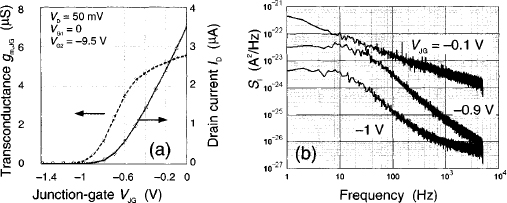
Figure 4. Volume mode operation of the G4-FET (VG1 = 0, VG2 = −9.5 V, VD = 50 mV): (a) measured drain current and transconductance as a function of the junction-gate voltage; (b) measured power spectral density of the drain current noise for various junction-gate voltages.4
4. Transition from volume noise to surface noise
The use of the G4-FET as a depletion-mode MOSFET enables the observation of the direct transition from volume to surface noise.9 We biased the G4-FET with a constant VJG and VG2, while sweeping VG1 to drive the front surface from depletion to strong accumulation. In Fig. 5 the resulting drain current noise power S![]() at 10 Hz is shown as a function of the drain current. Related current-voltage characteristics are plotted in the inset of Fig. 5 on a semilogarithmic scale.
at 10 Hz is shown as a function of the drain current. Related current-voltage characteristics are plotted in the inset of Fig. 5 on a semilogarithmic scale.
For VG1 = −2 V, transistor is in the off state because the depletion regions induced by the front, back and the junction-gates fully deplete the body. Until the flatband condition is reached, i.e., for −2 V < VG1 < 0.56 V or ID < 0.5 μA, the front-depletion region shrinks gradually and enables volume conduction, far from the front interface. In this region, the noise power follows the increase in current.
The striking aspect occurs around the onset of accumulation at the front surface (flatband condition), for ID = 0.5 μA: a very abrupt kink is observed in the noise amplitude. This kink is as large as one order of magnitude, due to the excess 1/f noise generated at the surface. The excess noise is explained by the dynamic capture/release of the carriers by the oxide traps located in the vicinity of the interface.3 The transition between the two modes of conduction (from volume to surface channel) which occurs at flatband voltage is clearly confirmed by the visible change in subthreshold slope (inset of Fig. 5) for the same current value.9

Figure 5. Drain current noise of the n-channel G4-FET. The kink corresponds to the onset of the front accumulation current that adds to the bulk component. Inset: related current-voltage characteristics.9
5. Bias dependence of the normalized current noise in surface and volume conduction modes
We studied the bias dependence of the G4-FET noise by monitoring the “total noise current” in a given frequency range ![]() , defined as:10,11
, defined as:10,11
Where Δf = fj+1 − fj is the bandwidth, fmin = f0 and fmax = fn are the minimum and maximum frequencies, respectively. As can be seen from Eq. (1), ![]() depends on the multiple noise PSD values measured between fmin and fmax, resulting in smoother variations of the noise power and more reproducible trends than an analysis based on a single frequency. Throughout the rest of this chapter we use Δf = 1 HZ, fmin = 1 HZ and fmax = 500 HZ for the total noise calculations.
depends on the multiple noise PSD values measured between fmin and fmax, resulting in smoother variations of the noise power and more reproducible trends than an analysis based on a single frequency. Throughout the rest of this chapter we use Δf = 1 HZ, fmin = 1 HZ and fmax = 500 HZ for the total noise calculations.
The variations of the “normalized total noise current”, ![]() , as a function of the drain current are often used for the noise spectroscopy. These characteristics make it possible to identify the noise sources starting from the experimental trends.13,14 In Fig. 6, we compare the normalized total noise current for the surface mode (top curve) and the volume mode with the front surface in depletion (middle curve) or in strong inversion (bottom curve).12 For all three cases in Fig. 6, the G4-FET operates in the subthreshold region for ID lower than 0.2−0.3 μA, and above threshold for a larger ID. This comparison unveils quantitative and qualitative features.
, as a function of the drain current are often used for the noise spectroscopy. These characteristics make it possible to identify the noise sources starting from the experimental trends.13,14 In Fig. 6, we compare the normalized total noise current for the surface mode (top curve) and the volume mode with the front surface in depletion (middle curve) or in strong inversion (bottom curve).12 For all three cases in Fig. 6, the G4-FET operates in the subthreshold region for ID lower than 0.2−0.3 μA, and above threshold for a larger ID. This comparison unveils quantitative and qualitative features.
![]() Noise reduction
Noise reduction
For a given drain current, ![]() is the highest in the surface mode, where the conducting channel is formed by electrons accumulated at the front interface. Here the current fluctuations are dominated by the intense exchange of majority carriers between the near-interface oxide traps and the channel. When the conducting channel is moved away from the surface towards the volume (volume mode, bottom two curves of Fig. 6), a substantial decrease in
is the highest in the surface mode, where the conducting channel is formed by electrons accumulated at the front interface. Here the current fluctuations are dominated by the intense exchange of majority carriers between the near-interface oxide traps and the channel. When the conducting channel is moved away from the surface towards the volume (volume mode, bottom two curves of Fig. 6), a substantial decrease in ![]() is observed due to the reduced amount of electron exchange between the conducting channel and the oxide traps. This is especially true when the front surface is in strong inversion: the exchange is almost completely suppressed because the top interface is “shielded” by the minority carriers (holes) and its effect on the bulk channel is minimized.15 This leads to a reduction of noise amplitude that may be larger than one decade compared to surface mode.
is observed due to the reduced amount of electron exchange between the conducting channel and the oxide traps. This is especially true when the front surface is in strong inversion: the exchange is almost completely suppressed because the top interface is “shielded” by the minority carriers (holes) and its effect on the bulk channel is minimized.15 This leads to a reduction of noise amplitude that may be larger than one decade compared to surface mode.
The low-noise feature of the volume conduction mode becomes more apparent when the noise is referred to the input.9,12 The total input-referred noise voltage, given by ![]() =
= ![]() , is a more significant parameter than
, is a more significant parameter than ![]() for the analog circuit design, since it takes into account the noise level and the gain of the transistor at the same time. In the volume conduction mode, the transconductance gm,JG is not degraded by the gate electric field, as is gm,G1 in the MOSFET mode above threshold – compare Fig. 4(a) and Fig. 3(a). This indicates a substantially lower
for the analog circuit design, since it takes into account the noise level and the gain of the transistor at the same time. In the volume conduction mode, the transconductance gm,JG is not degraded by the gate electric field, as is gm,G1 in the MOSFET mode above threshold – compare Fig. 4(a) and Fig. 3(a). This indicates a substantially lower ![]() in volume conduction mode, especially when the front interface is in inversion.9,12
in volume conduction mode, especially when the front interface is in inversion.9,12
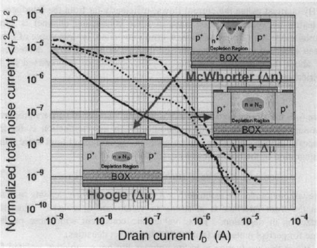
Figure 6. Normalized total noise current as a function of drain current in surface mode (dashed curve, VJG = −4 V), in volume mode with front surface in depletion (dotted curve, VG1 = 0) and in volume mode with front surface in strong inversion (solid curve, VG1 = −3 V). For all curves VG2 = 0, VD = 50 mV.12
In the surface mode, the ![]() vs. ID characteristic in Fig. 6 presents a plateau in the subthreshold region followed by a
vs. ID characteristic in Fig. 6 presents a plateau in the subthreshold region followed by a ![]() roll-off above threshold. Such a behavior is similar to that observed in inversion-mode MOSFETs and is consistent with the McWhorter’s carrier number fluctuation model.13,14
roll-off above threshold. Such a behavior is similar to that observed in inversion-mode MOSFETs and is consistent with the McWhorter’s carrier number fluctuation model.13,14
In MOSFETs, the noise power spectral density normalized to drain current is given by:
where SVG is the gate voltage spectral density, λox is an average tunneling length, W and L are the device width and length, Nt is the density of the slow oxide traps, and Cox, CD, qDit and Cinv are oxide, depletion, interface trap and inversion layer capacitances respectively. The factor η = 1 in weak inversion and 2 in strong inversion.16
By contrast, when the current flows sufficiently far from the interfaces and the interaction between the oxide traps and the conducting channel is suppressed (volume mode with front interface in strong inversion, bottom curve of Fig. 6), the plateau observed in surface conduction disappears and ![]() decreases as 1/ID over about three decades in current. This dependence is predicted by Hooge’s empirical relation:17
decreases as 1/ID over about three decades in current. This dependence is predicted by Hooge’s empirical relation:17
where ![]() H is the Hooge constant and N is the total number of carriers proportional to ID (assuming a bias-independent mobility when the conduction is far from the surfaces). Hooge’s equation can be adapted to normalized total noise current via an integration of the both sides of Eq. (3) from fmin to fmax:12
H is the Hooge constant and N is the total number of carriers proportional to ID (assuming a bias-independent mobility when the conduction is far from the surfaces). Hooge’s equation can be adapted to normalized total noise current via an integration of the both sides of Eq. (3) from fmin to fmax:12
In the volume mode, we estimate N = 4.5 ×10⁵ for ID = 6 μA, leading to ![]() H≅2×10⁻⁵ when the front interface is in strong inversion and
H≅2×10⁻⁵ when the front interface is in strong inversion and ![]() H ≅ 4×10⁻⁵ when the front interface is in depletion. These values are consistent with those predicted by Hooge for perfect materials (with negligible defect densities).17
H ≅ 4×10⁻⁵ when the front interface is in depletion. These values are consistent with those predicted by Hooge for perfect materials (with negligible defect densities).17
When the conduction is in the volume, but not completely isolated from the front-interface (JFET mode with the front interface depleted, middle curve of Fig. 6), the behavior of ![]() is a combination of trends implied by the McWhorter and Hooge models. This suggests a transition from the carrier number fluctuations to mobility fluctuations as the predominant noise mechanism when the conduction region is moved from the front surface to the volume of the G4-FET.12
is a combination of trends implied by the McWhorter and Hooge models. This suggests a transition from the carrier number fluctuations to mobility fluctuations as the predominant noise mechanism when the conduction region is moved from the front surface to the volume of the G4-FET.12
The difference between the top and bottom curves in Fig. 6 is the first experimental evidence of the paradigm shift between the two classical 1/f noise models. These models are not mutually exclusive because they can coexist in the same device. More studies are, however, necessary to fully confirm this conclusion because:
i) the type of G4-FET noise at low currents is not necessarily 1/f and it may present Lorentzian spectra as well (whereas the models developed by McWhorter and Hooge apply only to 1/f noise);
ii) the 1/ID noise variation seen for the volume conduction (volume mode with the front interface in strong inversion) that suggests agreement with Eq. (3) is no longer observed at relatively high currents (the slope deviates from 1/ID for ID > 2 μA and becomes the same as that of the surface current, as seen in Fig. 6, bottom curve). One possible explanation of this issue is the dominance of the noise generated by the back surface traps over the volume noise at high currents (note that in Fig. 6, VG2 = 0, making the back interface only slightly depleted).
Although further investigation is needed to appropriately model the characteristics presented above, there is no doubt concerning the intrinsic difference between the current dependence of the surface noise and the volume noise.12
6. Conclusion
The low-frequency noise characteristics of the G4-FET were investigated by distinguishing the surface and volume modes of operation. We observe 1/f noise in both surface and bulk conduction modes when the transistor is operated above threshold. The frequency exponent is higher at the surface than in the volume (1/f versus 1/f0.7). For a fixed drain current, the noise related to the volume of the transistor could be more than one decade lower than that generated at the surface. The G4-FET is a device where the intrinsic nature of the noise changes: the experimental results suggest a transition from McWhorter’s carrier number fluctuation model to Hooge’s mobility fluctuation model when the conducting channel is moved away from the front-interface towards the device center.
What about the conclusion of the noisy competition between the two camps? One set each.
References
- A. L. McWhorter, “1/f noise and germanium surface properties,” in: R. H. Kingston, ed., Semiconductor Surface Physics, Philadelphia: University of Pennsylvania Press, 1957, pp. 207–228.
- F. N. Hooge, “1/f noise is no surface effect,” Phys. Lett. A 29, 139 (1969).
- B. Dufrene, K. Akarvardar, S. Cristoloveanu, B. J. Blalock, P. Gentil, E. Kolawa, and M. M. Mojarradi, “Investigation of the four-gate action in G4-FETs,” IEEE Trans. Electron Dev. 51, 1931 (2004).
- K. Akarvardar, B. Dufrene, S. Cristoloveanu, J. A. Chroboczek, P. Gentil, B. J. Blalock, and M. M. Mojarradi, “Surface vs. bulk noise in SOI four-gate transistors,” Proc. IEEE Intern. SOI Conf. (2005), pp. 161–162.
- J. A. Chroboczek, “Automatic, wafer-level low frequency noise measurements for the interface slow trap density evaluation,” Proc. IEEE Intern. Conf. Microelectronics Test Structures (ICMTS) (2003), pp. 95–98.
- R. A. Wilcox, J. Chang, and C. R. Wiswanathan, “Low-temperature characterization of buried-channel NMOST,” IEEE Trans. Electron Dev. 36, 1440 (1989).
- J. Chang, C. R. Wiswanathan, and C. Anagnostopoulos, “Flicker noise measurements in enhancement mode and depletion mode NMOS transistors,” Proc. Intern. Symp. VLSI Technol. Syst. Applications (1989), pp. 217–221.
- S.-H. Ng and C. Surya, “A model for low-frequency excess noise in Si-JFETs at low bias,” Solid State Electronics 35, 1803 (1992).
- K. Akarvardar, S. Cristoloveanu, B. Dufrene, et al., “Evidence for reduction of noise and radiation effects in G4-FET depletion-all-around operation,” Proc. ESSDERC (2005), pp. 89–92.
- P. R. Gray and R. G. Meyer, Analysis and Design of Analog Integrated Circuits, 3rd ed., chapter 11, New York: Wiley, 1993.
- B. Razavi, RF Microelectronics, chapter 7, New York: Prentice-Hall, 1998.
- K. Akarvardar, B. Dufrene, S. Cristoloveanu, P. Gentil, B. J. Blalock, and M. M. Mojarradi, “Low-frequency noise in SOI four-gate transistors,” IEEE Trans. Electron Dev. 53, 829 (2006).
- J. Brini, “Low-frequency noise spectroscopy in MOS and bipolar devices,” Microelectronics Eng. 40, 167 (1998).
- G. Ghibaudo, O. Roux, Ch. Nguyen-Duc, F. Balestra, and J. Brini, “Improved analysis of the low frequency noise in field-effect MOS transistors,” Phys. Stat. Sol. 124, 571 (1991).
- T. Elewa, B. Boukriss, H. S. Haddara, A. Chovet, and S. Cristoloveanu, “Low-frequency noise in depletion mode SIMOX MOS transistors,” IEEE Truns. Electron Dev. 38, 323 (1991).
- S. Cristoloveanu and S. S. Li, Electrical Characterization of Silicon-On-Insulator Materials and Devices, chapter 9, Dordrecht: Kluwer Academic Publishers, 1995.
- F. N. Hooge, “1/f noise sources,” IEEE Trans. Electron Dev. 41, 1926 (1994).