1
History of MBE
Tom Foxon
Department of Physics and Astronomy, Nottingham University, Nottingham, NG7 2RD, UK
1.1 Introduction
John Orton and I have recently published a book entitled Molecular Beam Epitaxy – A Short History [1]. In that book we were not able to cover all aspects of this topic, so many significant contributions had to be omitted. In this short chapter, even more work of importance will be missing and what follows is my personal view of how molecular beam epitaxy (MBE) evolved. Before starting to describe how it occurred, we have of course to decide what we mean by MBE. As far as I can discover, the term was first used in the Proceedings of the Third International Symposium on GaAs and Related Compounds by Cho et al. [2] in order to distinguish MBE from the earlier growth methods, namely liquid phase epitaxy (LPE) and vapour phase epitaxy (VPE). So, what is MBE? One may consider it to be a refined form of vacuum evaporation, but it is clearly significantly different from simple evaporation in many ways. It usually involves multiple sources and deposition onto a heated substrate. It usually takes place in ultra‐high vacuum (UHV) equipment, in order to reduce the arrival rate of unwanted species. In general, collision‐free molecular beams are used to supply the required species to the substrate. It differs from many other growth methods in having many different in‐situ measurements (e.g. electron diffraction or mass spectrometry), which enables the process to be controlled at an atomic level. My personal view is that there are at least two MBE topics of equal importance, there is the study of the MBE process itself and the application of MBE to provide samples and devices of the highest possible quality. In my career I have been involved in both aspects for a variety of material systems and regard them as equally significant. In this chapter I will try to summarise what went into our book and will begin by discussing the development of the MBE process before turning to its application. Before starting on this task, I recommend to the reader two review articles published by three of the pioneers of MBE in 1974 [3] and 1975 [4], respectively. The first deals with epitaxy in general, whilst the second deals exclusively with MBE and gives a comprehensive account of the state of the art at that time (1975).
In what follows I will try to avoid too much overlap with the following chapters, so comments on devices, magnetic semiconductors and new materials will be very brief.
1.2 The MBE Process
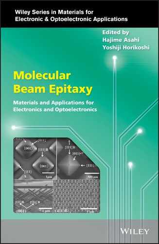
As far as I am aware, the first studies of growth, by what we now call MBE, were performed at Plessey Labs in Caswell by Bruce Joyce and co‐workers. They grew Si films from molecular beams of silane on a heated Si substrate under UHV conditions and the resulting samples were studied by Roger Booker at Cambridge University using transmission electron microscopy (TEM). This study was concerned with the nucleation process itself and very low growth rates were used in order to separate reactions on the surface from those in the gas phase, hence the need for collision‐free molecular beams. This work was published in a series of papers from 1966 onwards [5–7] and was summarised in a review article by Bruce Joyce in 1968 [8]. The equipment used for this study had many of the attributes of a modern MBE system (having collimated, collision‐free, molecular beams of silane impinging on a heated Si substrate) and took place under UHV conditions; the pressure during growth in the reaction chamber was ∼3 × 10⁻⁹ Torr. The growth rates were small compared to modern practise and no in‐situ characterisation was involved, but in all other respects this could be considered to be the first study of the MBE growth process. A result from this study is shown in Figure 1.1, where it is clear that Si grows epitaxially on the heated Si substrate by decomposition from the molecular beam of silane [8], in other words by MBE.
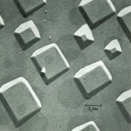
Figure 1.1 MBE deposition of Si from silane on a heated Si substrate under UHV conditions [8].
Following this initial work on Si, what followed was the use of MBE to grow compound semiconductors, mainly III–Vs and to a lesser extent II–VIs, motivated in part by the desire to produce semiconductor lasers. The initial work on lasers was carried out using LPE (for those interested in the development of solid‐state lasers, see the excellent book on the story of semiconductors [9]), but it soon became apparent that MBE could produce equivalent or better results. What followed was the development of MBE for many practical device applications, including lasers, transistors, and so on.
Shortly after the work at Plessey came the pioneering work at Bell Labs by John Arthur and co‐workers, who studied the interaction of molecular beams of gallium and arsenic on a heated GaAs substrate using in‐situ mass spectrometry [10]. This was followed by a study of the growth of GaAs, GaP and GaAsP by what he termed molecular beam deposition [11]. In his system the sources were surrounded by a liquid nitrogen‐cooled shroud and in‐situ mass spectrometry, Auger electron spectroscopy (AES) and low‐energy electron diffraction (LEED) were used for in‐situ analysis. The system also had provision for cleaning the substrate prior to growth using an argon ion gun. The mass spectrometer could be rotated to enable it to measure either the beams from the Knudsen cells or the species desorbing from the surface. From this study it became clear that for III–Vs the growth rate is controlled by the arrival rate of the group III species, providing there is an excess of the group V species. It also showed that the relative sticking coefficients for As and P are very different.
Shortly after Arthur's work at Bell Labs, Al Cho joined Morton B. Panish's group and embarked on his pioneering study of MBE. As everyone knows, he made outstanding contributions to both understanding the MBE process and its practical application for devices. His system had a reflection high‐energy electron diffraction (RHEED) system for surface analysis, an argon ion gun for surface cleaning, a cylindrical mirror analysis Auger system for surface composition and again the cells were mounted within a liquid nitrogen‐cooled shroud. The change from LEED to RHEED was crucial and enabled real‐time surface analysis, which has become the de‐facto standard in all modern MBE systems. I will discuss Al Cho's many contributions to the growth of structures for low‐dimensional structures and devices below, but here I wish to point out some of his critical contributions to understanding the MBE process. One of his most important contributions was to show, using RHEED, that for both the (111) [12] and (001) [13] surfaces a clear correlation exists between the surface structure we observe and both the III–V ratio and substrate temperature. The second paper [13] established the fact that under As‐rich conditions on the (001) surface we see a c(2 × 8) RHEED pattern, which becomes a c(8 × 2) pattern under Ga‐rich conditions; in between we also see other 6× patterns. This crucial observation enabled others to follow the process and establish the optimum III–V ratio and substrate temperature for growth. In 1971 he also published a paper showing how the RHEED pattern develops during growth from diffuse spots to streaks and at the same time the surface goes from rough to smooth [14]. This work was done long before atomic resolution of the surface by atomic force microscopy (AFM) became available and so the myth developed that streaky RHEED patterns correspond to atomically flat surfaces; this has become so ingrained in the literature that it is still stated as gospel today! Al Cho never said that and we know from first principles that RHEED streaks come from disorder on the surface and that an atomically smooth surface such as the Si(7 × 7) reconstruction will show sharp spots in the RHEED pattern [15].
In parallel with the work at Bell Labs, the IBM group also studied the growth of GaAs by MBE using RHEED. They showed how the various surface reconstructions related to the As2:Ga ratio and substrate temperature [16]. In that paper they make the statement that ‘The streaked RHEED pattern indicates smoothness on an atomic scale’, which is perhaps the origin of the myth surrounding RHEED streaks. This paper also mentions the use of a computer to control the MBE process, using data from the in‐situ mass spectrometer measurements.
Shortly after the pioneering work at Plessey, Bruce Joyce and Jim Neave moved to Mullards (later Philips) Research Laboratories at Redhill to work on the Si–SiO2 interface. I joined them in 1969 to do electron microscopy, but this proved impossible due to lack of equipment. At the same time there were difficulties with the VPE process and so collectively we set out to study the growth of GaAs by what became known as modulated beam mass spectrometry (MBMS) (see Figure 1.2). Our system was similar to that at Bell, but had the mass spectrometer mounted in a liquid nitrogen‐cooled cryopanel to improve the signal‐to‐noise ratio. We also used periodic modulation and Fourier transform techniques to extract the information, which included measurements of surface lifetime [17]. We first used this equipment to study the evaporation of GaAs under equilibrium and non‐equilibrium conditions as part of a PhD programme [18]. The results were essentially identical to those previously reported by John Arthur [19], which gave us confidence in our new approach. In a series of papers we then studied the growth of GaAs using As4 [20] and As2 [21], before studying alloys with mixed group III [22] and mixed group V species [23]. Again, this study confirmed earlier results from John Arthur, whilst adding additional information to the story. By that time MBE growth for devices was well established in several places and the emphasis switched to understanding MBE as opposed to VPE. A similar study for the growth of InP was also taking place at what was then the Royal Radar Establishment by Robin Farrow [24], who later made important contributions to understanding MBE of cadmium mercury telluride (CMT).
Figure 1.2 The system used at Mullards/Philips for modulated beam mass spectrometry measurements.
Probably one of the most important contributions to understanding the growth process in MBE was the discovery of oscillations in the RHEED pattern, which relate to the growth rate. This was first reported by Jeff Harris et al. [25], who saw this behaviour in Sn‐doped GaAs. Colin Wood states that he had previously observed such oscillations, but had not published this data [26]. As shown in Figure 1.3, it is now well established that the period of the oscillation corresponds to the deposition of a single monolayer of GaAs, as Harris and co‐workers proposed [25], but is now thought to arise from periodic changes in step density on the surface. Figure 1.4 shows a typical example of RHEED oscillations for AlAs and GaAs, and from such data it is possible to accurately predict the composition of AlGaAs alloys [27]. The origin of RHEED oscillations is generally now agreed to be associated with periodic changes in step density on the surface, as illustrated in Figure 1.5. This original picture in colour was drawn to explain this to the senior management at Philips and has been reproduced in many articles and books. The original is in my office.

Figure 1.3 Relation between the period of the oscillations and the growth rate in monolayers/second.
Source: This figure has been drawn using data taken from the original paper by Harris et al. [25].

Figure 1.4 Typical examples of RHEED oscillations for AlAs and GaAs courtesy of Dr Richard Campion. From such data it is possible to accurately measure the growth rates for both AlAs and GaAs and to predict the composition of AlGaAs alloys [27]. Note that the data is taken after any shutter transient has decayed (i.e. once the growth rate is constant with time).
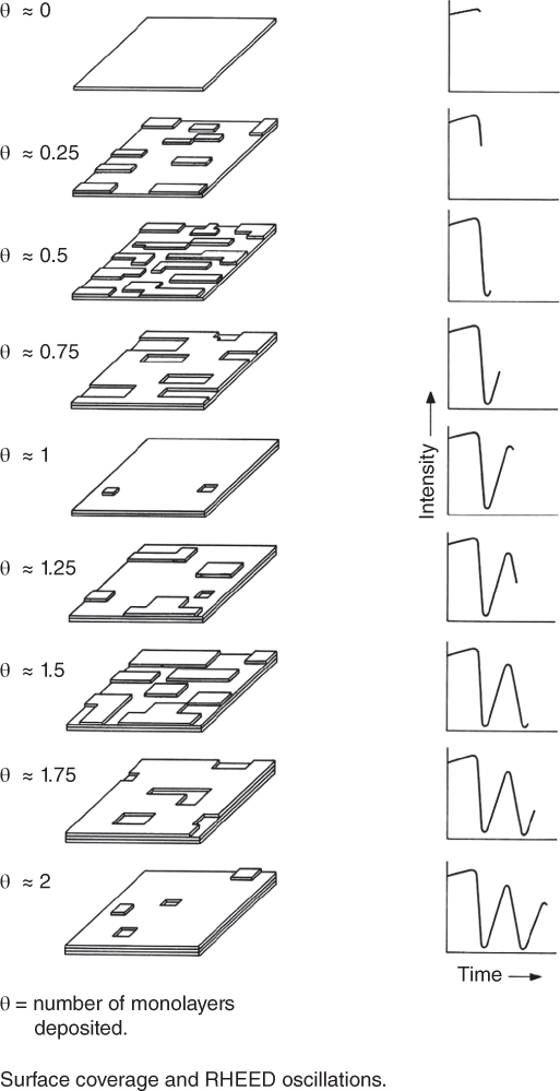
Figure 1.5 Model of film growth proposed by Joyce and co‐workers in 1986 starting from a flat surface. This model was used to explain RHEED oscillations to Philips managers who visited the lab. It has appeared in many articles, but the original remains in my office at Nottingham.
The growth of alloy films with mixed group III species is fairly straightforward, with the more volatile species determining the maximum growth temperature [22]. However, for alloys with mixed group V species the situation is more complex. The first studies by John Arthur and LePore [11] had shown that for GaAsP with equal beam intensities of As and P, approximately four times as much arsenic is incorporated compared to phosphorus. Our later MBMS studies confirmed the preferential incorporation of As over P [23]. Chang and co‐workers at IBM showed that for GaSbAs the incorporation of antimony is in preference to arsenic [28].
Thus, by the beginning of the 1980s most of the fundamental issues for the growth of III–V compounds and alloys had been resolved, but to make any reliable device, controlled n and p‐type doping is needed. Before discussing this, there is one final piece of the jigsaw which enabled the surface reconstruction to be related to the atomic structure of the surface. This came from the invention of scanning tunnelling microscopy (STM), which Mike Pashley and co‐workers used to study the GaAs(001)(2 × 4)–c(2 × 8) surface structure [29]. This showed that the 4× reconstruction is associated with missing dimers, which are aligned along the [−110] direction, thus giving rise to the 2× RHEED pattern observed [30]. Pashley later showed that this reconstruction can be predicted from an electron counting model, the missing dimers making the surface electrically neutral [31].
1.3 Controlled n and p Doping
In their 1975 review article [4], Cho and Arthur discussed doping by elements including Si, Ge, Sn, Mn, Te, Zn, C and Mg, each of which is a potential n or p‐type dopant.
For n‐type doping Sn gives the highest doping levels, but is subject to surface segregation [32], making sharp doping changes difficult. Si does not suffer from this problem and is generally a donor, except for growth on the (111)A, (211)A and (311)A surfaces [33], where p‐type conductivity is observed. Ge can also be used as either an n‐type or p‐type dopant, depending on the As:Ga ratio and temperature [34]. Of the three, Si is generally used for n‐type doping of III–Vs. Alternative approaches include the use of gas sources (e.g. SiH4 [35]), which avoids the use of a high‐temperature Si cell and again depends on growth parameters or the use of compound sources such as PbS, PbSe [36] or SnTe [37].
Historically, p‐doping proved more difficult to resolve; many of the traditional dopants (Zn, Cd, etc.) had very high vapour pressures and so were difficult to incorporate, others such as Mg had a very low sticking coefficient and diffused rapidly in GaAs. One solution to this problem was proposed by Naganuma and Takahashi [38], who used an ion source to improve the incorporation of Zn. Again, the solution came from Bell Labs with the proposal from Marc Ilegems to use Be as a p‐type dopant [39]. Later, C was used in metal‐organic MBE as a p‐type dopant by Weyers et al. [40] and later in MBE by Malik et al. [41], who used a heated graphite filament as the source of carbon.
In all the early work, changes in the doping level required adjusting either the dopant cell temperature or in some cases the substrate temperature, both rather slow processes. Wood et al. [42] introduced the idea of changing the doping level, by what they termed ‘atomic‐plane’ doping, and demonstrated this for GaAs, which led in turn to the concept of delta‐doping.
1.4 Modified Growth Procedures
To improve the properties of films grown by MBE, various modified procedures were used with a view in many cases to improving surface morphology and hence interface abruptness. It was clear from the early RHEED studies that on terminating growth, under the correct conditions, the RHEED intensity recovers. This method was used by Sakaki et al. [43] and Fukunaga et al. [44] to improve the quality of interfaces using growth interrupts.
A second application for RHEED came from the use of so‐called phase locked epitaxy. Again, two groups (Sano et al. [45] and Sakamoto et al. [46]) used RHEED to grow GaAs/AlAs superlattices with controlled thicknesses.
Briones et al. [47] modified this idea by interrupting only the group V species to provide the necessary enhanced migration for the group III species, again for growth at low substrate temperatures. They called this method nucleation‐enhanced molecular beam epitaxy (NEMBE) and compared the results with those obtained by migration‐enhanced epitaxy (MEE).
Another variant was introduced by Horikoshi et al. [48]. They found that if the group V flux is absent during the deposition of the group III species, it enhances diffusion, which gave rise to the term MEE. This method was especially relevant to growth at low substrate temperatures.
1.5 Gas‐Source MBE
The replacement of conventional solid sources by their gaseous equivalents began quite early with the work of Panish at Bell Labs, who used arsine and phosphine to grow GaAs and InP, respectively [49]. This was later extended to the growth of the quaternaries (Panish et al. [50]).
The first use of metal‐organics as a replacement was reported shortly after by Veuhoff et al. [51] in Germany and by Vodjani et al. [52] in France. In both cases, hydrides were also used for the group V species. The combination of metal‐organics with solid‐source arsenic came from Japan (Tokumitsu et al. [53]).
As noted above, the first use of gas sources for both species came from Veuhoff et al. [51], but major contributions to this came from later work at Bell Labs by Tsang [54]. In this work he used metal‐organics for both group III and group V sources, mainly to avoid the toxic hazards involved in the use of arsine and phosphine. He went on to apply this method to produce highly efficient double heterostructure lasers [55].
1.6 Low‐Dimensional Structures
A major contributor to the development of MBE came from the increasing interest in the physics and device possibilities associated with very thin films, where quantum effects become significant and tunnelling through barriers becomes possible, the so‐called low‐dimensional structures (LDS).
Prior to the development of MBE, growth of III–Vs by either VPE or LPE usually involved relatively thick layers of different composition. However, in 1970 at IBM Esaki and Tsu [56] proposed a new superlattice, which should show negative differential conductivity. This required very thin layers only a few monolayers thick. The existing growth methods did not seem suitable for this task and so they built the first computer‐controlled MBE system [57]. Using this system, they showed clear evidence for a composition profile of a periodic structure both by AES using ion beam sputter etching and by X‐ray interference showing satellite peaks [58].
This system showed clear evidence for negative resistance, thus confirming the theoretical predictions [16]. As an example, Figure 1.6 shows a typical superlattice grown by the present author at Philips Research Laboratories. The transmission electron micrograph was taken by my colleague Dr Jon Gowers. The IBM group also proposed resonant tunnelling through a double barrier structure [59] and again showed that this was in fact possible [60].

Figure 1.6 Example of a superlattice grown by MBE at Philips Research Laboratories UK as part of a programme on low‐threshold current lasers. The micrograph was taken by Dr Jon Gowers.
In 1974 Dohler spent some time at IBM where he worked with Esaki and became aware of the capability of MBE. On his return to Stuggart he worked with Ploog and together they developed the concept of a doping superlattice consisting of alternating layers of n and p‐type material with regions of intrinsic material in between, the so‐called n–i–p–i structure [61]. Even though the original idea was proposed by Dohler in 1972 [62], it took some time before the MBE technique became mature enough to realise practical devices; in particular, the development of p‐type doping by Be at Bell Labs [39] enabled the Stuggart group to realise such structures in practise.
An even greater stimulus to the development of MBE came from the development of quantum well (QW) structures. Again, Bell Labs were at the forefront of this development when, in 1974, Dingle et al. [63] discussed quantisation in thin AlGaAs/GaAs structures. One year later, Dingle produced an excellent review article discussing quantum confinement in ultra‐thin semiconductor structures [64], after which there was an explosion of work worldwide on such structures. In this type I QW structure the electrons and holes are both contained in the GaAs well, with a strong overlap of the electron and hole wave functions. However, it is possible to engineer a type II QW in which the electron confinement is in one material but the holes are confined to the barrier, thus increasing the radiative lifetime. This was first demonstrated by Dawson et al. [65], again at Bell Labs, during his year there on secondment. Finally, the ability to be able to programme and control the flux accurately in MBE enabled Miller et al. [66] to demonstrate the linear dependence of the confined states in a parabolic quantum well for the first time.
Two theoretical predictions from the University of Tokyo were to stimulate even more research into novel LDS. In the first paper, Sakaki [67] proposed that in a one‐dimensional structure there should be enhanced mobility due to suppression of scattering; he later proposed a reduced temperature dependence for the threshold current of QW lasers [68]. Both further stimulated research by MBE of LDS and low‐dimensional devices, including quantum wires and quantum dots.
Several novel approaches to achieving such structures included growth on high‐index 311 surfaces by Notzel et al. [69] at Stuggart and the cleaved‐edge overgrowth method developed by Pfeiffer et al. [70] at Bell Labs. Somewhat later, the first growth of nanowires by MBE was reported by Lee et al. [71] from Dongguk University in Korea. The more conventional approach of using gold nanoparticles was used by Ohlsson et al. [72] at Lund University, who used chemical beam epitaxy (CBE) for their samples.
The first demonstration of defect‐free quantum dots came from the work of Eaglesham and Cerullo [73] at Bell Labs, who showed by TEM defect‐free islands of Ge on Si grown by MBE. Later that same year, Guha et al. [74] at the University of California showed that defect‐free InAs islands could also be grown by MBE. In both cases the strain between the substrate and the layer is critical in transforming growth from two‐dimensional to three‐dimensional, resulting in quantum dot formation. There followed an intense discussion of the precise mechanism involved, which is described in some detail in the later review article by Joyce and Vvedensky [75].
Another major contributor to the success of MBE came from the discovery of modulation‐doped heterojunctions, where electron mobilities are enhanced by spatially separating the conducting channel from the dopants. This was first observed by Dingle et al. [76] at Bell Labs in an AlGaAs/GaAs multi‐quantum‐well structure and later in single heterojunction samples. The discovery of the two‐dimensional electron gas (2DEG) was followed by a demonstration of the two‐dimensional hole gas (2DHG) by Stormer and Tsang [77]. Following on from this initial work at Bell Labs there ensued an international race to improve the mobility, with the lead going from Japan to Europe and back to the USA. Some of the highest 2DEG mobilities were also obtained in Israel. The gradual improvements came from the introduction of the undoped spacer layer between the dopant and the 2DEG/2DHG and from a gradual improvement in both the source materials, the use of pre‐layers (including superlattices) and improvements to the MBE systems with extensive baking and improved pumping. While the original 2DHG was demonstrated in (001)‐oriented AlGaAs using Be as the dopant [77], using 311A‐oriented sample Si can act as an acceptor, thus improving the mobility [78].
Again this was partly driven by the discovery of the quantum Hall effect, which was first observed in silicon by Von Klitzing et al. [79] in 1980, who proposed a new resistance standard based on this discovery. In a search for the so‐called Wigner crystal, Tsui et al. [80] then discovered the fractional quantum Hall effect (FQHE) with a filling factor of one‐third.
Another driving force for the further improvement in mobility came from studies of ballistic transport in LDS, leading eventually to the observation of the quantised conductance of a quantum point contact [81,82].
In summary, the quest for new discoveries in LDS led to the development of MBE and to gradual improvements in the quality of the samples. Many of these new effects were first observed in samples grown by MBE.
1.7 III–V Nitrides, Phosphides, Antimonides and Bismides and Other Materials
Almost all of what is discussed above refers to III–As structures and there is no doubt that they were the most studied materials in the early history of MBE. However, other III–Vs, II–VIs, IV–VIs and SiGe were investigated to a smaller extent and more recently graphene and other two‐dimensional (2D) systems have been in vogue. It is clearly impossible to mention in this brief history all aspects of each and indeed, as noted in Section 1.1, other chapters in this book will cover much of this material in more detail. Accordingly, I will only mention the early papers in each case and hope this will be sufficient to encourage those interested to look in more detail at each topic.
1.7.1 III‐Nitrides
The interest in nitrides clearly came from the fact that they cover a very wide range of band gaps, from 0.7 eV for InN to 6.2 eV for AlN, thus covering all of the visible spectrum and into the deep ultraviolet and near infrared. The major stumbling blocks were lack of suitable lattice matched substrates and difficulty with p‐type doping. Nevertheless, there was considerable interest in nitrides from the MBE community, starting with the pioneering work in Japan of Yoshida et al. [83] in 1975 using a simple evaporation method. Later they developed what they termed reactive molecular beam epitaxy, which they used to study GaN/AlN heterostructures [84]. In this more sophisticated process, nitrogen was decomposed on the hot substrate from ammonia (NH3), Al was supplied from an e‐beam evaporator and Ga from a conventional effusion source. Using NH3, growth occurs under nitrogen‐rich conditions, usually the other III–Vs and later demonstrated growth of AlGaN alloys over the whole composition range from GaN to AlN [85]. They also showed that introducing an AlN buffer layer improved the quality of GaN grown on sapphire [86].
Various groups have continued to use ammonia as a source of active nitrogen, but there are well‐documented problems with this approach. An alternative is to use a plasma to excite nitrogen and form either atomic nitrogen or excited molecular nitrogen. Sato and Sato [87] used this method to grow InN, in their case using an RF coil in their evaporation system. The first MBE films using this method were grown by Davis's group in North Carolina using what became known as either plasma‐assisted (or plasma‐enhanced) MBE (PA‐MBE or PE‐MBE) [88]. In this work they used a microwave discharge in what became known as an electron cyclotron resonance (ECR) source. The same group also reported the first growth of BN films using a special high‐temperature source for boron [89].
An alternative approach was used by Hoke et al. [90] at Raytheon, who used the alternative RF plasma source from Oxford Applied Research to grow both InN and GaN (the RF plasma approach has now become the de‐facto standard for PA‐MBE). Various changes have allowed growth rates of several microns per hour to be obtained using this method, which we have used to grow thick free‐standing films of GaN, AlN and AlGaN [91].
Unlike other III–Vs, growth using a plasma source as opposed to ammonia requires a very different growth mode; growth under nitrogen‐rich conditions produces rough films, whilst growth under gallium‐rich conditions results in Ga droplet formation on the surface. However, growth in the intermediate regime results in relatively smooth surfaces and improved electrical properties [92]. However, growth under strongly nitrogen‐rich conditions does produce GaN nanocolumns, which are defect free. This growth mode was first reported by Yoshizawa et al. [93] from Sophi University, who grew GaN nanostructures by RF‐MBE directly on (0001) sapphire, without the use of any pre‐deposited metal droplets.
Finally, we should note that it is still not clear (at least to me) whether the active species are atomic or excited molecular nitrogen; there is excellent evidence for both, so it probably depends on the precise configuration of the source and may vary with both excitation power and nitrogen flow rate.
The interest in the meta‐stable form of cubic or the zinc‐blende form of nitrides stems from the fact that for (001)‐oriented films no electric fields are present, which can increase the overlap of electron and hole wave functions in QWs. The first report of the growth of cubic GaN came from Davis's group [89] and many groups have studied this type of GaN. In our case we used an arsenic flux to change the growth mode from wurtzite (hexagonal) to zinc‐blende (cubic) in a reproducible manner [94].
1.7.2 III‐Phosphides
The first reports of the growth of phosphide by MBE came from Bell Labs, where Arthur and LePore reported the growth of both GaAsP and GaP [11], shortly followed by Cho who grew GaP on CaF2 [95]. This early work involved growth using P4, but later alternative sources producing P2 were introduced to minimise the production of white phosphorus either by employing a thermal cracker (Wicks et al. [96]) or by dissociation of GaP (Yamane et al. [97]). The alloy (Al)GaInP can be lattice matched to GaAs and this could potentially be a route to red LEDs or lasers. The first reported growth of GaInP came from Philips (Mullards) Lab in Redhill by Scott and Roberts [98] and shortly after by Kawamura et al. [99] from the NTT Lab in Tokyo. One year later the NTT group also reported on the growth of the quaternary AlGaInP, again lattice matched to GaAs [100].
The prospect of growing III–V structures on Si could potentially be used to combine the best of both worlds. The first step towards this came from the growth of GaP on Si, where there is only a small mismatch in lattice parameter. This was first reported by Gonda et al. [101]. One of the key issues here is to avoid anti‐phase domain boundaries, which in turn require double steps on the Si substrate, which was solved much later by Grassman et al. [102] using a quite complex procedure.
1.7.3 III‐Antimonides
As with the phosphide and arsenides, there was very early work on the growth of antimonides starting with the IBM group, who grew GaSbAs lattice matched to InGaAs [103]. Shortly after this the group at Waseda University reported the growth of both GaSb and GaSbAs [104]. Much of the work in this area involved the growth of GaSb:InAs heterostructures, where there is no common anion, thus alloying the formation of either As‐like or Sb‐like interfaces. The differences were studied in detail by Tuttle et al. [105] much later for InAs:AlSb quantum wells; they found significant differences in both carrier density and mobility.
1.7.4 III‐Bismides
The current interest in bismides comes from the incorporation of small amounts in GaAs, which rapidly narrows the band gap, but the original motivation involved incorporation of small amounts of Bi in InSb for far‐infrared detectors by the Westinghouse group [106]. Much later, in a collaborative effort between the National Renewable Energy Lab in the USA and the University of British Columbia in Canada, Bi incorporation into GaAs was shown to rapidly narrow the band gap, with up to a few percent Bi incorporation under close to stoichiometric conditions [107]. Thai work was in part motivated by the earlier growth by metal‐organic vapour phase epitaxy (MOVPE), where small amounts of Bi were incorporated [108].
1.7.5 Highly Mismatched Alloys
Alloys where a much larger or smaller atom is incorporated in a host (e.g. N in GaAs) produced the surprising result that instead of a linear dependence of the band gap from, in this case, GaN to GaAs, there is an extreme bowing of the band gap, which was not predicted by theory until it was first observed experimentally. In 1992, Baillargeon et al. [109] in Illinois showed this behaviour for GaPN and in the same year, using plasma‐assisted MOVPE, Weyers et al. [30] at NTT saw similar behaviour in GaAsN. Later, Kondo et al. [110] at Hitachi showed that a similar effect is seen in MBE, again using a plasma source for nitrogen. This general trend in highly mismatched alloys was then explained by Shan et al. [111] using the band anti‐crossing (BAC) model.
In both cases above the larger P or As atom was displaced by the much smaller N atom, giving rise to bowing. In the case of Bi the opposite case also shows a rapid decrease in band gap, so this is a general trend. To incorporate large amounts requires low growth temperatures, as we have shown for GaN with As, P or Sb, where even when the material becomes first polycrystalline and finally amorphous, there is still excellent agreement between the theoretical predictions of the BAC and experimental data (see e.g. Yu et al. [112]).
1.7.6 II–VIs
The II–VI compounds and alloys have energy gaps covering all of the visible spectrum and indeed some have negative gaps, some crystallise in the zinc‐blende form and others are wurtzite. Thus in principle they have a wide variety of possible applications. However, a major difficulty in II–VIs was controlled n and p‐type doping, since many contained high levels of unintentional impurities. Nevertheless, early in the development of MBE the group at Perkin Elmer reported the growth of CdSe, CdTe, ZnSe and ZnTe [113]. Their dual‐chamber system introduced the samples via a preparation/analysis chamber, which included a LEED/Auger system for surface analysis and in‐line mass spectrometry in the growth chamber, but without real‐time monitoring with RHEED. In the II–VIs, careful control of stoichiometry is needed and in a later paper they did succeed in showing controlled n and p‐type doping of II–VIs using Bi and Tl, respectively [114].
At almost the same time the group at the Electrotechnical Laboratory studied the growth of ZnTe by MBE and found that they could obtain twin‐free growth at substrate temperatures between 360 and 400 °C [115]. Later the same group reported the first observation of RHEED oscillations for II–VI films grown by MBE [116].
The problem of p‐type doping for ZnSe grown by MBE was finally improved by the introduction of nitrogen doping using a plasma source [117]. This followed on from previous studies of N doping by ion implantation [118].
Although the wide‐band‐gap II–VIs initially showed great promise for blue/green LEDs, the nitrides developed by MOVPE took over this activity. However, one area where the II–VIs remained competitive was for CMT, which was first grown by MBE in France at the LETI/CENG laboratory near Grenoble [119]. After much development this has now become a commercial product and MBE proved suitable for this technology [120].
1.7.7 IV–VIs
T. Ford Holloway et al. [121] first grew lead tin telluride by vacuum evaporation in 1970, but later progressively refined this to become MBE (see the review by Walpole [122] for details). Perhaps the first report of growth by MBE as we understand it now came from the Perkin‐Elmer work by Smith and Pickhardt [123]. They later also used the system described above for II–VIs to grow IV–VIs by MBE to obtain low‐doped films [124]. Later, Walpole et al. [125] at Lincoln Labs used MBE to produce PbSnTe lasers able to operate CW up to 114 K. Even now there are some groups working in this field, but the number of groups working on IV–VIs by MBE is limited compared to those working on III–Vs.
1.7.8 SiGe
Once again the early work involved two Bell Labs, who in 1977 both commenced work on Si MBE [126,127]. Both groups continued to study MBE for many years and their papers are highly cited in the literature. Si was provided from an e‐beam source. Both groups studied Sb for n‐type doping, as the conventional dopants (As and P) have high vapour pressure. For p‐type doping, Al and Ga were used [126]. Later, Ota [128] introduced ion beam doping with As. The use of an e‐beam source enabled Bean and Sadowski [129] to achieve extremely high growth rates, up to 20 µm h−1 [comparable to the chemical vapour deposition (CVD) process used in Si technology].
At much the same time, both AEG Telefunken and Hitachi also started programmes in this area. Konig et al. [130] used MBE to grow Si, again using Sb as the n‐type dopant. Again, an e‐beam source was used for Si and a conventional Knudsen source for Sb. This paper also refers to their earlier work on the growth of SiGe and SiGe SLs by what they termed UHV epitaxy, which to all intents and purposes is MBE by another name [131]. For this study again the Si came from an e‐beam source and the Ge from a Knudsen cell.
At Hitachi, Katayama et al. [132] reported a metal‐oxide field effect transistor, where they compared a device prepared on Si grown by MBE with one prepared by the conventional method. They concluded that the mobility of the Si grown by MBE is comparable to that obtained by the usual method. They also commented that this avoids any problems produced by ion implantation and thermal treatment. At NTT, Sugiura [133] also studied doping in Si MBE using ion doping to obtain accurate control of the Sb doping profile.
Following on from the work on Si it was natural to consider alloys with Si and in particular SiGe. This resulted in a number of interesting observations, including the fact that the critical layer thickness could be greater than the existing theory predicted, leading People and Bean [134] to propose a more accurate theory for samples with very low dislocation density.
The first 2DHG and 2DEG were also reported by People et al. [135] and Abstreiter et al. [136], respectively. In due course Si/SiGe HBTs were also grown and reported by four groups in 1988, but competition from the existing CVD technology meant that as far as I am aware, this never reached production.
Finally we should mention MBE growth of SiC alloys, which was first reported by Miyazawa et al. [137] in 1984. In this case the Si was evaporated from an e‐beam source and an ion beam was used for carbon. Slightly later, Kaneda et al. [138] used e‐beam sources for both Si and C. In 1992 Yoshinobu et al. [139] grew 3C SiC on 6H SiC using gas source MBE. In this case alternating supplies of disilane and acetylene were used to grow monolayers of Si and C to produce SiC.
1.7.9 2D Materials
The discovery of graphene by ex‐foliation in 2004 produced a high interest in 2D materials in general, and since then many have been discovered. For those interested in the history of this new family of materials, I recommend two recent articles which may be of interest [140,141].
The growth of 2D films is possible due to the absence of dangling bonds in this family of materials; work on such growth by MBE started as early as 1884 and is generally known as van der Waals epitaxy. Due to the lack of strong interlayer bonding, despite a large difference in lattice parameter, defect‐free material can be obtained (as discussed by Koma [142], who was one of the pioneers in this area of MBE). Despite the lack of interlayer bonding the various layers are oriented in‐plane, giving rise to moiré patterns in AFM or STM images [143]. In our recent studies of the high‐temperature growth of graphene on hexagonal boron nitride, such patterns can clearly be seen by STM [144].
1.8 Early MBE‐Grown Devices
Many groups worldwide were quick to see the potential of MBE for device applications, but there can be no doubt that the early work at Bell Labs by many researchers including, most especially, Al Cho stimulated interest in this aspect of MBE. In Section 1.1 I mentioned the early review by Cho and Arthur who summarised the situation in 1975 for devices produced using MBE, and that article will provide the reader with an excellent summary [4].
It is often said that other epitaxial techniques (CVD and MOVPE) are more appropriate for production, but there are areas where MBE has taken the lion's share of the market (e.g. power transistors for mobile phones and quantum cascade lasers, to name but two).
1.9 Summary
MBE has come a long way since I first became involved in the late 1960s, with pioneering efforts worldwide. A whole community of researchers have contributed to this development and continue to do so in many different aspects of the work. For those whose work I have failed to mention, I can only plead lack of space!
Acknowledgments
I wish to acknowledge all the help I have received over the years from colleagues all around the world and in particular to thank Professor Orton with whom I prepared the book on the history of MBE and also my close colleagues here at Nottingham – Professor Novikov, Dr Campion and Dr Cheng – with whom I have worked since arriving.
References
- 1 Orton, J.W. and Foxon, C.T. (2015). Molecular Beam Epitaxy – A Short History. Oxford: Oxford University Press.
- 2 Cho, A.Y., Panish, M.B., and Hayashi, I. (1970). Proceedings of the Third International Symposium on GaAs and Related Compounds, vol. 18. London: Institute of Physics. ISBN: 0854980148.
- 3 Joyce, B.A. (1974). Rep. Prog. Phys. 37: 363.
- 4 Cho, A.Y. and Arthur, J.R. (1975). Prog. Solid State Chem. 10: 157.
- 5 Joyce, B.A. and Bradley, R.R. (1966). Philos. Mag. 14: 289.
- 6 Booker, G.R. and Joyce, B.A. (1966). Philos. Mag. 14: 301.
- 7 Joyce, B.A., Bradley, R.R., and Booker, G.R. (1967). Philos. Mag. 15: 1167.
- 8 Joyce, B.A. (1968). J. Cryst. Growth 3: 43.
- 9 Orton, J.W. (2004). The Story of Semiconductors. Oxford: Oxford University Press.
- 10 Arthur, J.R. (1968). J. Appl. Phys. 39: 4032.
- 11 Arthur, J.R. and LePore, J.J. (1969). J. Vac. Sci. Technol. 6: 545.
- 12 Cho, A.Y. (1970). J. Appl. Phys. 41: 2780.
- 13 Cho, A.Y. (1971). J. Appl. Phys. 42: 2074.
- 14 Cho, A.Y. (1971). J. Vac. Sci. Technol. 8: S31.
- 15 Ichimura, A. and Cohen, P.I. (2004). Reflection High Energy Electron Diffraction. Cambridge: Cambridge University Press.
- 16 Chang, L.L., Esaki, L., Howard, W.E. et al. (1973). J. Vac. Sci. Technol. 10: 655.
- 17 Foxon, C.T., Boudry, M.R., and Joyce, B.A. (1974). Surf. Sci. 44: 69.
- 18 Foxon, C.T., Harvey, J.A., and Joyce, B.A. (1973). J. Phys. Chem. Solids 34: 1693.
- 19 Arthur, J.R. (1967). J. Phys. Chem. 28: 2257.
- 20 Foxon, C.T. and Joyce, B.A. (1975). Surf. Sci. 50: 434.
- 21 Foxon, C.T. and Joyce, B.A. (1977). Surf. Sci. 64: 293.
- 22 Foxon, C.T. and Joyce, B.A. (1978). J. Cryst. Growth 44: 75.
- 23 Foxon, C.T., Joyce, B.A., and Norris, M.T. (1980). J. Cryst. Growth 49: 132.
- 24 Farrow, R.F.C. (1974). J. Phys. D7: 114.
- 25 Harris, J.J., Joyce, B.A., and Dobson, P.J. (1981). Surf. Sci. Lett. 108: L90.
- 26 Wood, C.E.C. (1981). Surf. Sci. 108: 441.
- 27 P. J. Dobson, C. T. Foxon and J. H. Neave, Patent Applications US19830552653 19831117, GB198220033778
- 28 Chang, C., Ludeke, R., Chang, L.L., and Esaki, L. (1977). Appl. Phys. Lett. 31 (759).
- 29 Pashley, M.D., Haberern, K.W., Friday, W. et al. (1988). Phys. Rev. Lett. 60: 2176.
- 30 Weyers, M., Sato, M., and Ando, H. (1992). Jpn. J. Appl. Phys. 31: L853.
- 31 Pashley, M.D. (1989). Phys. Rev. B 40: 10481.
- 32 Wood, C.E.C. and Joyce, B.A. (1978). J. Appl. Phys. 49: 4854.
- 33 Wang, W.I., Mendez, E.E., Kuan, T.S., and Esaki, L. (1985). Appl. Phys. Lett. 47: 826.
- 34 Cho, A.Y. and Hayashi, I. (1971). J. Appl. Phys. 42: 4422.
- 35 Briones, F., Golmayo, D., Gonzalez, L., and de Miguel, J.L. (1985). J. Vac. Sci. Technol. B3: 568.
- 36 Wood, C.E.C. (1978). Appl. Phys. Lett. 33: 770.
- 37 Collins, D.M. (1979). Appl. Phys. Lett. 35: 67.
- 38 Naganuma, M. and Takahashi, K. (1975). Appl. Phys. Lett. 27: 342.
- 39 Ilegems, M. (1977). Appl. Phys. Lett. 48: 1278.
- 40 Weyers, M., Putz, N., Heineke, H. et al. (1986). J. Electron. Mater. 15: 57.
- 41 Malik, R.J., Nottenberg, R.N., Schubert, E.F. et al. (1988). Appl. Phys. Lett. 53: 2661.
- 42 Wood, C.E.C., Metze, G., Berry, J., and Eastmann, L.F. (1980). J. Appl. Phys. 51: 383.
- 43 Sakaki, H., Tanaka, M., and Yoshino, J. (1985). Jpn. J. Appl. Phys. 24: L417.
- 44 Fukunaga, T., Kobayashi, K.L.I., and Nakashima, H. (1985). Jpn. J. Appl. Phys. 24: L510.
- 45 Sano, N., Kato, H., Nakayama, M. et al. (1984). Jpn. J. Appl. Phys. 23: L640.
- 46 Sakamoto, T., Funabashi, H., Ohta, K. et al. (1984). Jpn. J. Appl. Phys. 23: L657.
- 47 Briones, F., Gonzalez, L., Recio, M., and Vazquez, M. (1987). Jpn. J. Appl. Phys. 26: L1125.
- 48 Horikoshi, Y., Kawashima, M., and Yamaguchi, H. (1986). Jpn. J. Appl. Phys. 25: L868.
- 49 Panish, M.B. (1980). J. Electrochem. Soc. 127: 2729.
- 50 Panish, M.B., Temkin, H., and Sumski, S. (1985). J. Vac. Sci. Technol. B3: 657.
- 51 Veuhoff, E., Pletschen, W., Balk, P., and Luth, H. (1981). J. Cryst. Growth 55: 30.
- 52 Vodjani, N., Lemarchand, A., and Paradan, H. (1982). J. Phys. C5: 339.
- 53 Tokumitsu, E., Kudou, Y., Konagai, M., and Takahashi, K. (1884). J. Appl. Phys. 55: 3163.
- 54 Tsang, W.T. (1984). Appl. Phys. Lett. 45: 1234.
- 55 Tsang, W.T. and Miller, R.C. (1986). J. Cryst. Growth 77: 55.
- 56 Esaki, L. and Tsu, R. (1970). IBM J. Res. Dev. 14: 61.
- 57 Chang, L.L., Esaki, L., Howard, W.E. et al. (1973). J. Vac. Sci. Technol. 10: 11.
- 58 Esaki, L. and Chang, L.L. (1976). Thin Solid Films 36: 285.
- 59 Tsu, R. and Esaki, L. (1973). Appl. Phys. Lett. 22: 562.
- 60 Chang, L.L., Esaki, L., and Tsu, R. (1974). Appl. Phys. Lett. 24: 593.
- 61 Dohler, G.H. and Ploog, K. (1979). Prog. Cryst. Growth Charact. Mater. 2: 145.
- 62 Dohler, G.H. (1972). Phys. Status Solidi B52: 533.
- 63 Dingle, R., Wiegman, W., and Henry, C.H. (1974). Phys. Rev. Lett. 33: 827.
- 64 Dingle, R. (1975). Festkorperprobleme XV: 21.
- 65 Dawson, P., Wilson, B.A., Tu, C.W., and Miller, R.C. (1986). Appl. Phys. Lett. 48: 541.
- 66 Miller, R.C., Gossard, A.C., Kleinman, D.A., and Munteanu, O. (1984). Phys. Rev. B29: 3740.
- 67 Sakaki, H. (1980). Jpn. J. Appl. Phys. 19: L735.
- 68 Arakawa, Y. and Sakaki, H. (1982). Appl. Phys. Lett. 40: 939.
- 69 Notzel, R., Ledentsov, N.N., Daweritz, L. et al. (1992). Phys. Rev. B45: 3507.
- 70 Pfeiffer, L., West, K.W., Stormer, H.L. et al. (1990). Appl. Phys. Lett. 56: 1697.
- 71 Lee, H.G., Jeon, H.C., Kang, T.W., and Kim, T.W. (2001). Appl. Phys. Lett. 78: 3319.
- 72 Ohlsson, B.J., Bjork, M.T., Magnusson, M.H. et al. (2001). Appl. Phys. Lett. 79: 3335.
- 73 Eaglesham, D.J. and Cerullo, M. (1990). Phys. Rev. Lett. 64: 1943.
- 74 Guha, S., Madhukar, A., and Rajkumar, K.C. (1990). Appl. Phys. Lett. 57: 2110.
- 75 Joyce, B.A. and Vvedensky, D.D. (2004). Mater. Sci. Eng., R 46: 127.
- 76 Dingle, R., Stormer, H.L., Gossard, A.C., and Wiegmann, W. (1978). Appl. Phys. Lett. 33: 665.
- 77 Stormer, H.L. and Tsang, W.T. (1980). Appl. Phys. Lett. 36: 685.
- 78 Wang, W.I., Mendez, E.E., Iye, Y. et al. (1986). J. Appl. Phys. 60: 1834.
- 79 Von Klitzing, K., Dorda, G., and Pepper, M. (1980). Phys. Rev. Lett. 45: 494.
- 80 Tsui, D.C., Stormer, H.L., and Gossard, A.C. (1982). Phys. Rev. Lett. 48: 1559.
- 81 Wharam, D.A., Thornton, T.J., Newbury, R. et al. (1988). J. Phys. C21: L209.
- 82 Van Wees, B.J., Kouwenhoven, L.P., Van Houten, H. et al. (1988). Phys. Rev. B38: 3625.
- 83 Yoshida, S., Misawa, S., and Itoh, A. (1975). Appl. Phys. Lett. 26: 461.
- 84 Yoshida, S., Misawa, S., and Gonda, S. (1983). J. Vac. Sci. Technol. B1: 250.
- 85 Yoshida, S., Misawa, S., and Gonda, S. (1982). J. Appl. Phys. 53: 6844.
- 86 Yoshida, S., Misawa, S., and Gonda, S. (1983). Appl. Phys. Lett. 42: 427.
- 87 Sato, Y. and Sato, S. (1989). Jpn. J. Appl. Phys. 28: L1641.
- 88 Paisley, M.J., Sitar, Z., Posthill, J.B., and Davis, R.F. (1989). J. Vac. Sci. Technol. A7: 701.
- 89 Paisley, M.J., Sitar, Z., Yan, B., and Davis, R.F. (1990). J. Vac. Sci. Technol. B8: 323.
- 90 Hoke, W.E., Lemonias, P.J., and Weir, D.G. (1991). J. Cryst. Growth 111: 1024.
- 91 Novikov, S.V., Kent, A.J., and Foxon, C.T. (2017). Prog. Cryst. Growth Charact. Mater. 63: 25.
- 92 Heying, B., Smorchkova, I., Poblenz, C. et al. (2000). Appl. Phys. Lett. 77: 2885.
- 93 Yoshizawa, M., Kikuchi, A., Nori, M. et al. (1997). Jpn. J. Appl. Phys. 36: L459.
- 94 Cheng, T.S., Jenkins, L.C., Hooper, S.E. et al. (1995). Appl. Phys. Lett. 66: 1509.
- 95 Cho, A.Y. (1970). J. Appl. Phys. 41: 782.
- 96 Wicks, G.W., Koch, M.W., Varriano, J.A. et al. (1991). Appl. Phys. Lett. 59: 342.
- 97 Yamane, K., Kobayashi, T., Furakawa, Y. et al. (2009). J. Cryst. Growth 311: 794.
- 98 Scott, G.B. and Roberts, J.S. (1979). Inst. Phys. Conf. Ser. 45: 181.
- 99 Kawamura, Y., Asahi, H., and Nagai, H. (1981). Jpn. J. Appl. Phys. 20: L807.
- 100 Asahi, H., Kawamura, Y., and Nagai, H. (1982). J. Appl. Phys. 53: 4928.
- 101 Gonda, S., Matsushima, Y., Mukai, S. et al. (1978). Jpn. J. Appl. Phys. 17: 1043.
- 102 Grassman, T.J., Brenner, M.R., Rajagopalan, S. et al. (2009). Appl. Phys. Lett. 94: 232106.
- 103 Sakaki, H., Chang, L.L., Ludeke, R. et al. (1977). Appl. Phys. Lett. 31: 211.
- 104 Yano, M., Suzuki, Y., Ishii, T. et al. (1978). Jpn. J. Appl. Phys. 17: 2091.
- 105 Tuttle, G., Kroemer, H., and English, J.C. (1990). J. Appl. Phys. 67: 3032.
- 106 Noreika, A.J., Takei, W.J., Francombe, M.H., and Wood, C.E.C. (1982). J. Appl. Phys. 53: 4932.
- 107 Francoeur, S., Seong, M.J., Macarenhas, A. et al. (2003). Appl. Phys. Lett. 82: 3874.
- 108 Oe, K. and Okamoto, H. (1998). Jpn. J. Appl. Phys. 37: L1283.
- 109 Baillargeon, J.N., Pearah, P.J., Cheng, K.Y. et al. (1992). J. Vac. Sci. Technol. B10: 829.
- 110 Kondo, M., Uomi, K., Hosomi, K., and Mozume, T. (1994). Jpn. J. Appl. Phys. 33: L1056.
- 111 Shan, W., Walukiewicz, W., Ager, J.W. et al. (1999). Phys. Rev. Lett. 82: 1221.
- 112 Yu, K.M., Novikov, S.V., Broesler, R. et al. (2009). J. Appl. Phys. 106: 103709.
- 113 Smith, D.L. and Pickard, V.Y. (1975). J. Appl. Phys. 46: 2366.
- 114 Smith, D.L. and Pickard, V.Y. (1978). J. Electrochem. Soc. 125: 2042.
- 115 Yao, T., Amano, S., Makita, Y., and Maekawa, S. (1976). Jpn. J. Appl. Phys. 15: 1001.
- 116 Yao, T., Taneda, H., and Funaki, M. (1986). Jpn. J. Appl. Phys. 25: L952.
- 117 Park, R.M., Mar, H.A., and Salansky, N.M. (1985). J. Appl. Phys. 58: 1047.
- 118 Wu, Z.L., Merz, J.L., Werkhoven, C.J. et al. (1982). Appl. Phys. Lett. 40: 345.
- 119 Faurie, J.P. and Million, A. (1981). J. Cryst. Growth 54: 582.
- 120 Norton, P. (2002). Opto‐Electron. Rev. 10: 159.
- 121 Holloway, H., Logothetis, E.M., and Wilkes, E. (1970). J. Appl. Phys. 41: 3543.
- 122 Holloway, H. and Walpole, J.N. (1979). Prog. Cryst. Growth Charact. Mater. 2: 49.
- 123 Smith, D.L. and Pickhardt, V.Y. (1975). J. Electron. Mater. 4: 1256.
- 124 Smith, D.L. and Pickhardt, V.Y. (1976). J. Electron. Mater. 5: 247.
- 125 Walpole, J.N., Calawa, A.R., Harman, T.C., and Groves, S.H. (1976). Appl. Phys. Lett. 28: 552.
- 126 Becker, G.E. and Bean, J.C. (1977). J. Appl. Phys. 48: 3395.
- 127 Ota, Y. (1977). J. Electrochem. Soc. 124: 1795.
- 128 Ota, Y. (1979). J. Electrochem. Soc. 126: 1761.
- 129 Bean, J.C. and Sadowski, E.A. (1982). J. Vac. Sci. Technol. 20: 137.
- 130 Konig, U., Kibbeland, H., and Kasper, E. (1979). J. Vac. Sci. Technol. 16: 985.
- 131 Kasper, E., Herzog, H.J., and Kibbel, H. (1975). Appl. Phys. 8: 199.
- 132 Katayama, Y., Shiraki, Y., Kobayashi, K.L.I. et al. (1979). Appl. Phys. Lett. 34: 740.
- 133 Sugiura, H. (1980). J. Appl. Phys. 51: 2630.
- 134 People, R. and Bean, J.C. (1985). Appl. Phys. Lett. 487: 322.
- 135 People, R., Bean, J.C., Lang, D.V. et al. (1984). Appl. Phys. Lett. 45: 1231.
- 136 Abstreiter, G., Brugger, H., Wolf, T. et al. (1985). Phys. Rev. Lett. 54: 2441.
- 137 Miyazawa, T., Yoshida, S., Misawa, S., and Gonda, S. (1984). Appl. Phys. Lett. 45: 380.
- 138 Kaneda, S., Sakamoto, Y., Nishi, C. et al. (1986). Jpn. J. Appl. Phys. 25: 1307.
- 139 Yoshinobu, T., Mitsui, H., Izumikawa, I. et al. (1992). Appl. Phys. Lett. 60: 824.
- 140 Castellanos‐Gomez, A. (2016). Nat. Photonics 10: 202.
- 141 Bhimanapati, G.R., Lin, Z., Meunier, V. et al. (2015). ACS Nano 9: 11509.
- 142 Koma, A. (1999). J. Cryst. Growth 201/202: 236.
- 143 Parkinson, B.A., Ohuchi, F.S., Ueno, K., and Koma, A. (1991). Appl. Phys. Lett. 58: 472.
- 144 Cheng, T.S., Davies, A., Summerfield, A. et al. (2016). J. Vac. Sci. Technol. B34: 02L101.