13
III‐Nitride Quantum Dots for Optoelectronic Devices
Pallab Bhattacharya Thomas Frost Shafat Jahangir Saniya Deshpande and Arnab Hazari
Department of Electrical Engineering and Computer Science, University of Michigan, Ann Arbor, MI 48109, USA
13.1 Introduction
Recent demand for visible and ultra‐violet light‐emitting diodes (LEDs) and lasers is immense, due to their numerous applications in the fields of solid‐state lighting, optical data storage, plastic fiber communication, full‐color mobile projectors, heads‐up displays, and in quantum cryptography and computing [1,2]. Most research and development into these light sources is being done using nitride‐based materials, where the emission can be tuned from deep ultra‐violet in AlN (∼6 eV) to the near infrared by using InN (∼0.7 eV). Since the first report of a blue‐emitting InGaN/GaN quantum well (QW) LED in 1995 [3], much progress has been made in extending the emission to longer wavelengths through the incorporation of more indium in the InGaN QWs [4–11]. While the first blue‐emitting laser was demonstrated by Nakamura in 1996 [12], it has since become increasingly difficult to grow and fabricate lasers at longer wavelengths. It was only as recently as 2009 that the first green‐emitting laser was demonstrated using InGaN/GaN QWs [13], and red emission has yet to be achieved with QWs. To fully realize the potential of these nitride‐based LEDs and lasers, it is necessary to further extend the emission wavelength of these devices beyond green into the red, which will allow for the production of solid‐state projectors and white light sources from a single material system.
The large indium composition and associated strain in the ternary InGaN QWs lead to clustering effects and a large piezoelectric polarization field, especially in c‐plane heterostructures, both of which are detrimental to device performance. The threshold current density of lasers is generally very large due to reduced electron–hole (e–h) wavefunction overlap in the QWs [ 4–6,8, 9,11,14, 15]. Additionally, a large blue shift of the emission peak with injection is observed due to the quantum confined Stark effect (QCSE) associated with the polarization field [13]. It has been shown that material inhomogeneities and the piezoelectric field increase in InGaN/GaN QWs with increasing indium content. Further, a wider well width that is needed for emission at longer wavelengths is not an option, since the band bending due to a strong polarization field reduces e–h wavefunction overlap significantly. It is for these reasons that a “green gap” exists in the output spectrum of III‐nitride‐based light emitters and that red‐emitting LEDs and lasers with InGaN/GaN QWs have not yet been demonstrated. InGaP/InGaA1P double‐heterostructure and QW lasers lattice matched to GaAs and emitting in the red wavelength region of 650–670 nm have been reported [16–18]. However, these devices are characterized by very large values (5–10 kA cm−2) and strong temperature dependence (T0 ∼ 50–100 K) of the threshold current density. Both of these characteristics are detrimental in real high‐performance applications.
Self‐assembled InGaN/GaN quantum dots (QDs) can be epitaxially grown in the Stranski–Krastanow (SK) growth mode [19–24]. These dots are formed by the relaxation of strain and it has been shown both theoretically [25,26] and experimentally [ 19–23] that the piezoelectric field and the resultant QCSE are significantly lower than those values reported for comparable QWs. As a result, the radiative carrier lifetimes in such dots are typically around 10–100 times smaller than those in equivalent QWs [21]. Furthermore, the quasi‐three‐dimensional confinement of carriers in the InGaN islands that form the dots can reduce carrier migration to, and therefore recombination at, dislocations and other defects. While these advantages (reduced polarization and non‐radiative recombination) are unique to nitride‐based quantum dots, they also have many of the same advantages of quantum dots demonstrated with other material systems. The incorporation of self‐organized quantum dots in GaAs and InP‐based heterostructures has resulted in superior device performance [27–29]. In(Ga)As QD lasers have extremely small threshold current density, wide tunability of the output wavelength, large modulation bandwidth, and near‐zero chirp and linewidth enhancement factor [28].
In this chapter we focus on the molecular beam epitaxy (MBE) of red‐emitting SK self‐organized quantum dots and their application to white LEDs and diode lasers. A detailed description of plasma‐assisted molecular beam epitaxy (PAMBE) and characterization of the quantum dots is given in Section 13.2. A monolithic all‐semiconductor converter white LED incorporating blue‐and red‐emitting quantum dots is described in Section 13.3. The epitaxy and properties of quantum dot lasers are described in Section 13.4. The chapter concludes in Section 13.5.
13.2 Molecular Beam Epitaxy of InGaN/GaN Self‐organized Quantum Dots
High‐quality III‐nitride materials and heterostructures have been demonstrated using a variety of growth techniques including metal‐organic chemical vapor deposition (MOCVD) [30], hydride vapor‐phase epitaxy (HVPE) [31], and MBE [7, 19 21– 23,25, 26]. HVPE is widely used for the growth of bulk GaN layers due to the very large growth rate (∼50 μm h−1), while quantum confined heterostructures are typically grown by MOCVD [ 4, 6 8– 11]. As an alternative to these two techniques, MBE provides several important advantages. First, the typical growth temperature is 100–200 °C lower than that in MOCVD growth, which is favorable for increasing the indium incorporation in epitaxy layers. This is particularly useful for long‐wavelength light emitters (beyond 530 nm), where InxGa1−xN with x ≥ 0.4 is required. Additionally, this allows for the growth of high‐quality lattice‐matched In0.18Al0.82N layers, improving the optical confinement in such long‐wavelength devices [21]. A second inherent advantage is the relatively high vacuum environment, which suppresses the incorporation of impurities in epitaxial layers. Third, the growth rate in MBE can be precisely controlled at the submonolayer level, allowing for the precise control needed for the growth of quantum dots. Finally, in‐situ monitoring including reflection high‐energy electron diffraction (RHEED) allow for improved control during the growth.
Epitaxial growth for our work was carried out in a Veeco Gen II PAMBE system. In this growth technique, active nitrogen species are generated in a plasma tube. In contrast to ammonia‐based MBE, the amount of active nitrogen species is independent of growth temperature and depends on the flow rate of nitrogen into the plasma source and radio frequency (RF) power. The plasma source used in the experiments presented in this work is a Veeco UNI‐bulb source and operates with a 13.6 MHz RF source with a maximum output power of 600 W. Nitrogen purity is carefully controlled at 99.99999 purity. After excitation, ionized species in the plasma include N2+, N, and N+, which all contribute to the formation of GaN [32].
Molecular beam epitaxial growth usually occurs in the surface kinetic limited regime [33]. Adatom surface diffusion and desorption are important parameters during growth and are largely controlled by adjusting the substrate temperature. The substrate temperature was measured with an infrared pyrometer, calibrated by the RHEED transition in Si (111). The RHEED pattern remains (7 × 7) below 850 °C and changes to (1 × 1) above this temperature. Thermocouple temperatures are calibrated according to this transition. Substrate temperatures quoted here were calculated through this calibration.
Quantum dot‐like nanostructures can be realized by a number of techniques, including anti‐surfactant‐assisted growth, annealing of thin epitaxial InGaN layers, interrupted growth mode during deposition of InGaN, and selective growth. Quantum dots have also been realized by post‐growth‐controlled etching of InGaN/GaN QWs [34].
Nakajima et al. have calculated thickness–composition phase diagrams for Frank and van der Merwe (FM), Stranski–Krastanow (SK), and Volmer–Weber (VW) growth modes of InGaN on finite‐sized (0001)‐oriented GaN [35]. The particular growth mode depends on the alloy composition, strain distribution in the heterostructure, defect density, and adatom kinetics on the (0001) surface. In general, the layer‐by‐layer FM growth mode is not favored for large In compositions. The SK island growth of self‐assembled InGaN/GaN quantum dots can be achieved when a relatively large lattice mismatch exists between the InGaN layer and the underlying layer (usually GaN). A two‐dimensional wetting layer is formed before the generation of three‐dimensional islands. The VW growth mode results in the formation of 3D islands, without a 2D wetting layer, when a large lattice mismatch is present (larger than required for SK growth). This growth mode has recently been shown to be the dominant one causing the formation of 3D quantum dots in InGaN disks of high In content inserted in GaN nanowires [36]. These nanowires usually grow in the wurtzite crystalline form on Si substrates.
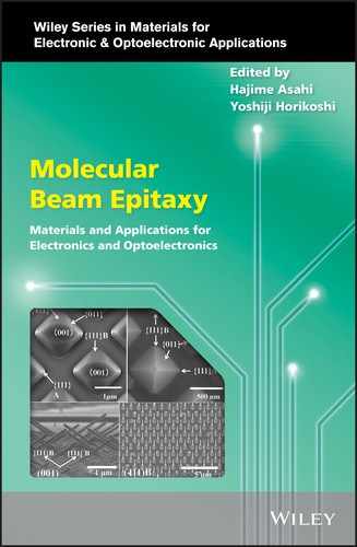
While the epitaxy of InGaN/GaN quantum dots has been reported by various groups [ 21, 29 36–40], detailed characterization of their growth phenomena had not been done. In growing multiple quantum dot layers, with suitable barrier layers in between, it is often assumed that the layers of quantum dots are near identical. In our study, we have grown GaN‐based heterostructures with multiple dot layers, which are typically incorporated in the active region of LEDs and lasers. The test structures were grown on GaN‐on‐sapphire substrates. An undoped GaN buffer layer of 500 nm thickness was first grown at 710 °C with a Ga flux of 2.2 × 10⁻⁷ Torr and with 0.66 sccm of ultra‐high purity N2 with a plasma source power of 350 W. In0.4Ga0.6N/GaN quantum dots were then grown at 540 °C under nitrogen‐rich conditions (1.33 sccm/420 W N2 plasma power). Single or multiple dot layers with a nominal InGaN thickness of 12 monolayers (MLs) and alternating GaN barriers of 12 nm thickness were grown, usually with an interruption after the growth of a dot layer. Nominal values of In and Ga fluxes for an In composition of 40% in the QD are 9 × 10⁻⁸ and 4 × 10⁻⁸ Torr, respectively. The average alloy composition in the QD along the c‐axis is measured by energy dispersive X‐ray spectroscopy on a suitably prepared transmission electron microscopy (TEM) sample, which shows a variation in the alloy composition along the c‐axis with a maximum In content of ∼40% for red‐emitting QDs (Figure 13.1). The composition measured by X‐ray diffraction in a relaxed bulk layer with the same nominal composition is similar. Unlike what is observed during the growth of InGaAs quantum dots [41], it is found by atomic force microscopy (AFM) that the first layer of QDs has a smaller dot density (∼7 × 107 cm−2), which increases in the second layer and remains relatively constant at 5 × 1010 cm−2 in the third and higher layers. AFM images from the first four layers are shown in Figure 13.2. The increase in dot density can clearly be observed in these images, with the lowest density in the first layer. The dot height and density are shown quantitatively in Figure 13.3. The dot height follows a trend very similar to that seen in the area densities, with an increase from the first to the third layer, followed by a saturation of the height. Interestingly, the dot base width is roughly constant in all these samples. The average base width under these growth conditions is 37 ± 5 nm, with a variation of 5 nm. The change in island density from the first quantum dot layer to the second can be understood by considering how In surface segregation impacts the critical thickness for island nucleation in these layers. The resulting composition profile can be understood following the work of Dehaese [42]. The critical thickness is greatest for the first quantum dot layer. Consequently, the first layer of dots requires more deposited material to reach Ucr than do subsequent layers. Since each layer is exposed to the growth flux for the same amount of time, the first layer of dots has a shorter amount of time over which the islands grow. The island density is proportional to the product of the island growth time and the nucleation rate. Thus, the first layer will have a lower island density, assuming that the nucleation rate is constant.
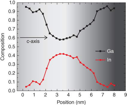
Figure 13.1 Variation in the In and Ga compositions across a red‐emitting InGaN/GaN self‐organized quantum dot measured by energy dispersive X‐ray spectroscopy. The underlying image is the annual dark‐field image of the quantum dot.
(Source: After Frost et al. [21].)
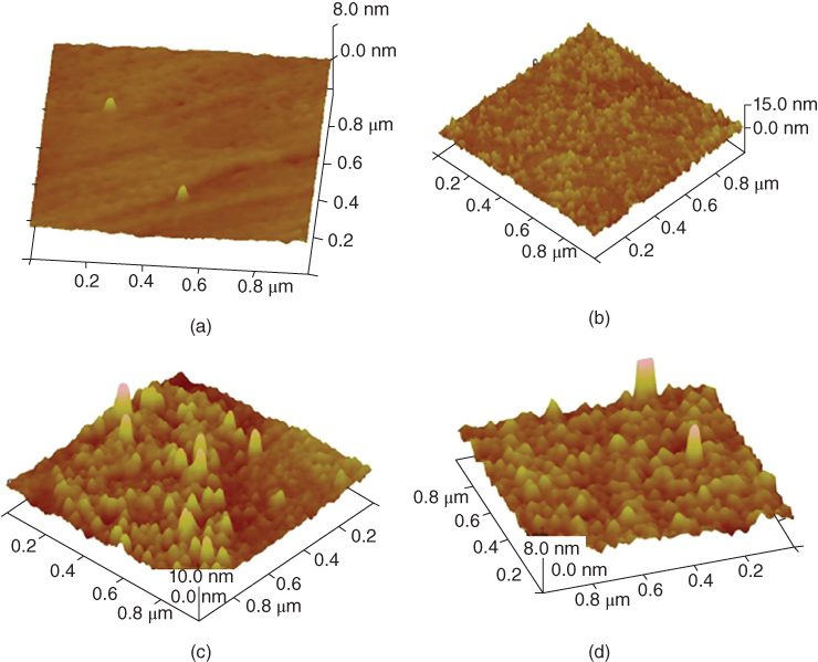
Figure 13.2 Atomic force microscopy images of uncapped layers of InGaN/GaN quantum dots. The numbers of uncapped layers used for the heterostructure are (a) 1, (b) 2, (c) 3, and (d) 4.
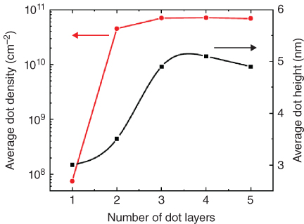
Figure 13.3 InGaN island height and aerial density derived from the AFM imaging on the samples shown in Figure 13.2.
(Source: After Frost et al. [24].)
The relatively low density of quantum dots on the first layer has several important consequences on heterostructures which incorporate these dots into the active region. First, the very low fill factor will result in a negligible contribution of this first layer to the modal gain of a laser, which is a product of the material gain and the optical confinement factor. While the first layer provides minimal contribution to the modal gain, it can be used in other applications including single photon sources which have recently been reported [43]. Additionally, due to low density, individual dots can be imaged by AFM, as shown in Figure 13.4. Figure 13.4(a, b) shows plan view images of the two dots in Figure 13.2(a). Clear hexagonal symmetry can be observed in these dots. However, the dots are sometimes elongated in one direction. Further analysis is required to determine the facets of these dots and the direction of the elongation. A side view of an InGaN island is shown in Figure 13.4(c), revealing that the dots grow into a truncated pyramid.
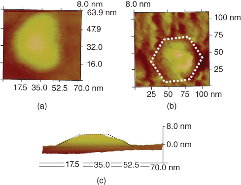
Figure 13.4 Atomic force microscopy images of the single dots shown in Figure 13.2(a). The dots generally form a truncated hexagonal pyramid. In some of the dots (a), the island may be elongated and not a regular hexagon.
It is also observed that the growth of the QDs follows a kinetics‐driven scaling law, in accordance with the observations made by Amar et al. [33]. Under this kinetically driven growth model, adatoms on the surface may not reach their thermodynamically favored state and instead are limited by the amount of kinetic energy and mobility they have on the surface, to be incorporated into the lattice. Island formation and stability are determined by the size of the island. Smaller islands will be relatively unstable with fewer bonds. At some critical island size, represented by the variable i, dots will typically be stable. Figure 13.5(a) shows the line shape, or scaling function of the size (height) distribution for InGaN/GaN dots grown at 545 °C, measured by AFM. The data obtained from the top layer of a seven‐layer stack have been analyzed with the scaling function
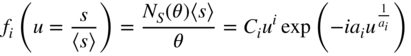

Figure 13.5 (a) Distribution of InGaN island heights for typical red‐emitting quantum dots. The solid line is the best fit of the scaling function to the measured AFM data; (b) scaling functions showing the best fit to this data is i = 5 at a growth temperature of 545 °C. Note that a higher value of i means higher uniformity.
(Source: After Frost et al. [24].)
where Ns is the size distribution, s is the island size, and θ is the coverage. It is found that the value of i increases from 3 to 5 with increase in substrate temperature from 440 to 545 °C [17]. For comparison, AFM data related to several of these scaling functions are shown in Figure 13.5(b). A lower value of i also implies a less uniform distribution of quantum dots. This may be one limitation to realizing longer‐wavelength quantum dot devices (beyond red). Sufficient modal gain from a single state may not be reachable unless the uniformity can be increased.
13.2.1 Optical Properties
In order to understand the radiative recombination processes in the quantum dots, temperature dependent and time‐resolved photoluminescence (PL) measurements were made on the laser heterostructure shown in Figure 13.6, etched down to the p‐InGaN waveguide layer above the quantum dots. Temperature‐dependent PL spectra are shown in Figure 13.7(a). The peak emission energy in the spectra closely follows the Varshni equation [44] with increasing temperature, shown in Figure 13.7(b). No “S‐shaped” behavior [45,46], usually attributed to compositional non‐uniformity and clustering, is observed. The temperature‐dependent PL measurements were also performed at high excitation levels and the radiative efficiency of In0.4Ga0.6N/GaN quantum dots was estimated from the ratio of the peak intensities at 300 and 30 K to be ∼36%.

Figure 13.6 Quantum dot laser heterostructure grown by MBE on (0001)GaN substrate for photoluminescence measurements.
(Source: After Frost et al. [21].)

Figure 13.7 (a) Typical photoluminescence spectra of red‐emitting InGaN/GaN quantum dots as a function of temperature; (b) variation of peak emission energy from the red‐emitting In0.4Ga0.6N/GaN quantum dots as a function of temperature. The solid line is a fit to the data with the Varshni relation for the given values of α and β; (c) photoluminescence decay transient measured at room temperature.
(Source: After Frost et al. [21].)
Time‐resolved PL measurements were made on the quantum dot heterostructures as a function of temperature. The transient data at room temperature, shown in Figure 13.7(c), was analyzed with the stretched exponential model
where τ is the lifetime and β is the stretching parameter. Values of τ and β of 810 ps and 0.95, respectively, are derived. This value of β suggests a small polarization field and non‐uniformity in the dots. From the measured τ and ηi, values of the radiative and non‐radiative lifetimes are calculated to be 2.2 and 1.3 ns, respectively, at room temperature using

Values of τr and τnr were similarly calculated from temperature‐dependent TRPL data. These are plotted, together with the values of τ, in Figure 13.8(a). It is observed that the radiative lifetime increases with temperature, in contrast to the expected trend of a constant value, as seen in bulk materials and QWs. The increase in radiative lifetime with increasing temperature has been previously observed in InGaAs/GaAs self‐organized QDs [48]. The anomalous behavior was explained by invoking e–h scattering, instead of phonon scattering, as the dominant mechanism to cool high‐energy electrons to the ground state [49]. The electron states in the QDs are discrete, in contrast to other systems, and the separation between them can exceed the LO phonon energy (phonon energies of InN: 86 meV and GaN: 91 meV), presenting a phonon bottleneck. In contrast, there is a continuum of hole states due to degeneracy and band mixing. Occupation of the low‐lying electron states, which participate in the luminescence process, depends on e–h scattering and hole occupation of the ground state. In e–h scattering, shown schematically in Figure 13.8(b) for low temperatures, hot electrons scatter with cold ground‐state holes and relax to the ground state. The energy gained by the holes excites them to higher energy levels, from which they can relax rapidly by multi‐phonon emission. With increase of temperature, the thermal excitation of cold holes from the ground state will leave fewer holes to scatter with hot electrons, and the rate of e–h scattering and electron relaxation to the ground state decreases. This results in an increase of the radiative lifetime. The same processes are likely operative in the InGaN/GaN self‐organized QDs being investigated here.

Figure 13.8 (a) Variation of carrier lifetimes in In0.4Ga0.6N quantum dots with temperature; (b) schematic representation of electron–hole scattering. Electron states are discrete and may be separated by energies unobtainable from phonons. Scattering with cold holes is required for electrons to relax into the ground state. This process becomes less efficient at higher temperatures as the supply of cold holes is reduced.
(Source: After Deshpande et al. [47].)
13.3 Quantum Dot Wavelength Converter White Light‐Emitting Diode
We have demonstrated high‐performance blue‐ and green‐emitting LEDs having multiple quantum dot layers in the active recombination region [20,50]. Since red‐emitting quantum dots can easily be grown, a converter white LED, which incorporates both blue‐ and red‐emitting QDs in a single heterostructure, is of more interest. The most common approach for realizing a solid‐state white LED is to have a blue‐emitting LED optically pump yellow phosphor [51,52]. However, phosphor‐converted white LEDs have shortcomings. The conversion is accompanied by losses due to Stokes shift and non‐radiative internal losses [53]. Backscattering of both pump and converted light by the phosphor gives rise to optical loss. Heating and the long‐term reliability of the phosphor are also detrimental factors [54–57]. In the following, we will describe a white LED with a monolithic semiconductor‐based wavelength converter.
The InGaN/GaN QD white LED heterostructure, shown in Figure 13.9, was grown by PAMBE on c‐plane GaN‐on‐sapphire templates. A n‐doped (5 × 1018 cm−3) 300 nm GaN buffer layer was first grown at 720 °C. Multiple layers of self‐organized InGaN/GaN QDs with 12 nm GaN barrier layers were grown as the long‐wavelength converter over the n‐GaN buffer layer under nitrogen rich condition at 541–550 °C. This was followed by the growth of 150 nm n‐GaN layer (n ∼ 7.5 × 1018 cm−3) at 720 °C, multiple exciting InGaN/GaN QD layers with 16 nm GaN barrier layers for blue emission grown at T = 585–592 °C, 15 nm p‐Al0.15Ga0.85N electron blocking layer (EBL), and finally a 120 nm p‐GaN (p ∼ 7 × 1017 cm−3) layer grown at 680 °C. The number of exciting and converter dot layers was carefully optimized to obtain true white emission.

Figure 13.9 Schematic of InGaN/GaN quantum dot wavelength converter white LED heterostructure grown by MBE.
(Source: After Jahangir et al. [58].)
We will describe here the characteristics of one white LED in more detail. This device contains three excitation (pump) In0.24Ga0.76N dot layers with peak emission at 450 nm and five converter In0.38Ga0.62N dot layers emitting at 615 nm. The blue‐emitting dot layers were grown at 585 °C with In and Ga fluxes of 3.7 × 10⁻⁸ and 1.57 × 10⁻⁷ Torr, respectively. The red‐emitting dot layers were grown at 541 °C with In and Ga fluxes of 1.18 × 10⁻⁷ and 9.94 × 10⁻⁸ Torr, respectively. The radiative efficiency of the blue‐ and red‐emitting dots are 52% and 42%, respectively. The blue dots have average height, base width, and area density of 3 nm, 30 nm, and ∼4 × 1010 cm−2, respectively, while these parameters for the red converter dots are 4 nm, 40 nm, and ∼3.5 × 1010 cm−2, respectively.
Mesa‐shaped LEDs of dimension 600 × 600 μm2 were fabricated using standard photolithography, reactive ion etching (RIE), and ohmic contact metallization techniques. Carriers are injected electrically into the blue‐emitting InGaN/GaN QD layers and the emission from these dot layers optically excites the red‐emitting converter dots to produce white light. An Al reflector layer is deposited on the backside sapphire surface.
The measured electroluminescence spectra for varying injection levels are shown in Figure 13.10(a). The two peaks at 450 and 615 nm correspond to the exciting (active) blue and converter red dots, respectively. From the small shifts of the emission peaks with injection, the polarization fields in the blue‐ and red‐emitting dots are calculated to be 82 and 170 kV cm−1, respectively. The light–current (L–I) characteristics and the corresponding variation in external quantum efficiency (EQE) are shown in Figure 13.10(b). The efficiency reaches a maximum at the low injection of 37 A cm−2 and the reduction in EQE at an injection of 100 A cm−2 is ∼15%. The chromaticity diagram of the LED, derived from electroluminescence data, is shown in Figure 13.10(c). The correlated color temperature (CCT) varies from 4375 to 4585 K with injection varying from 25 to 100 A cm−2. The small change in CCT with injection is attributed to the small polarization in the dots and corresponding small blue shift with injection.
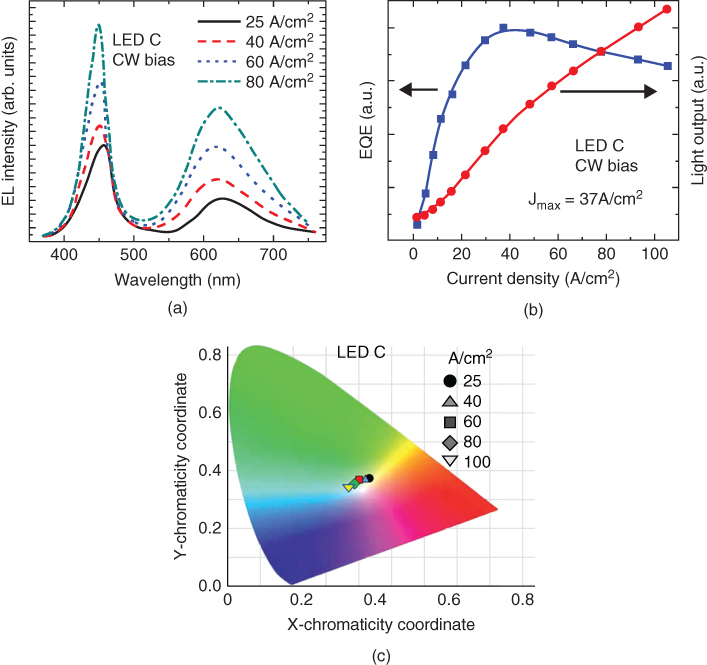
Figure 13.10 (a) Electroluminescence of a while LED as a function of injection current density; (b) light–current characteristics and external quantum efficiency of the same LED under continuous wave biasing; (c) trend of chromaticity coordinates of white light emission from device of Figure 13.9 with variation of injection current density.
(Source: After Jahangir et al. [58].)
By varying the number of dot layers and peak emission of the exciting and converter dots, we have been able to measure CCT in the range of 4420–6700 K, at a fixed injection of 45 A cm−2. The desirable CCT for cool white light is ∼4500 K. The values of the CCT measured in the QD converter white LED would be very difficult to achieve in all QW converter LEDs, since it is difficult to obtain emission at 600 nm or higher. It should be possible in the future to design QD converter LEDs with CCT ∼3000 K to obtain warm white light. This would be achieved by extending the emission peak of the converter dots to longer wavelengths.
13.4 Quantum Dot Lasers
We reported the first InGaN/GaN quantum dot laser [19]. With peak emission at λ ∼ 524 nm (green), the laser had a measured threshold current density of 1.2 kA cm−2 and slope and wall‐plug efficiencies of 0.74 W A−1 and 1.1%, respectively. This was followed by the demonstration of blue‐emitting (λ ∼ 420 nm) QD lasers, with similar characteristics [20]. While blue‐ and green‐emitting lasers have been demonstrated with InGaN/GaN QWs, the QD lasers have significantly smaller thresholds, which exhibit a weak temperature dependence (large value of T0). It is of more interest to examine the properties of QD lasers emitting at longer wavelengths, which cannot be achieved with QWs. In the following, we describe the steady‐state and dynamic characteristics of InGaN/GaN QD lasers emitting at ∼630 nm.
13.4.1 Epitaxy of InAlN and QD Laser Heterostructure
The QD heterostructure for lasers emitting at ∼630 nm is shown in Figure 13.11. It is important to note that the more commonly used AlGaN waveguide cladding layers are replaced by the alloy In0.18Al0.82N lattice‐matched to GaN. The use of this material, which provides a large index step compared with lattice‐mismatched AlGaN, in the cladding significantly improves confinement of the optical modes at the longer wavelengths. This leads to reduced cavity loss due to free carrier absorption from the reduced overlap of the optical mode with the heavily doped cladding. Additionally, substrate leakage will also be reduced, further minimizing the cavity loss. The optical confinement provided by In0.18Al0.82N is comparable to that of Al0.46Ga0.54N [59]. The growth of this alloy was done under varying growth conditions to optimize its optical and structural characteristics. Due to the low incorporation of indium at high temperatures, the growth must be done at a relatively low substrate temperature, while ensuring that the temperature is sufficiently high to prevent a rough surface morphology from high aluminum adatom sticking coefficient (∼1), and to avoid low carrier mobilities. Another advantage of the relatively low growth temperatures (compared with TSUB ∼ 740 °C for AlGaN) is that the growth of the upper cladding layer can be done at a temperature lower than the quantum dot growth temperature. This reduces high‐temperature annealing and outdiffusion of indium from the dots, which may prevent the realization of long waveguide devices. X‐ray diffraction rocking curves of three samples grown at 469, 497, and 510 °C are shown in Figure 13.12(a–c), respectively. Varying the substrate temperature over this relatively small range results in a large increase of indium composition from 14% (at 510 °C) to 30% (at 469 °C). At 497 °C, lattice‐matched In0.18Al0.82N can be grown with a smooth surface morphology, as shown in the AFM image in Figure 13.12(d).
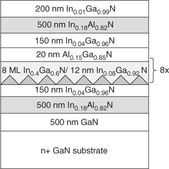
Figure 13.11 InGaN/GaN quantum dot laser heterostructure grown on (0001)GaN substrate by MBE.

Figure 13.12 X‐ray diffraction rocking curves for InAlN with growth temperatures (a) 469 °C, (b) 497°C, and (c) 510 °C; (d) atomic force microscopy image of lattice‐matched In0.18Al0.82N on (0001)GaN.
(Source: After Frost et al. [21].)
To improve the optical confinement, the GaN barrier layers and waveguides were replaced with In0.08Ga0.92N, and In0.04Ga0.96N, respectively, which also resulted in an increase of the QD internal quantum efficiency to 51%. Eight In0.42Ga0.58N/In0.08Ga0.92N QD layers have been incorporated into the laser heterostructure to maximize the confinement factor and gain. Adding more dot layers increases the possibility of generating dislocations, increasing the threshold current density, and non‐uniform hole injection. The optical confinement factor, calculated by the transfer matrix method, is 0.075 and the QD fill factor is 0.38. The top p‐In0.01Ga0.99N contact layer has a doping of 5 × 1017 cm−3, and the last 100 nm of this layer was grown by metal modulated epitaxy to yield higher doping level. The laser diodes have a turn‐on voltage of 2.7–3.3 V, a series resistance of ∼6 Ω, and a reverse leakage current of 6.6 mA at −5 V. Ridge waveguide edge‐emitting lasers of various cavity dimensions were fabricated using standard photolithography, dry etching, and metallization techniques. The ridge is etched down to the waveguide/cladding heterointerface to minimize cavity loss associated with sidewall roughness. End mirrors are formed by cleaving the device along the m‐plane and coating the cleaved facets with TiO2/SiO2 distributed Bragg reflectors (DBRs), to give reflectivities of ∼0.7 and 0.95. All laser measurements described in the following correspond to the output from the low‐reflectivity facet. No special device mounting or heat sinking was implemented in these measurements.
13.4.2 Steady‐State Laser Characteristics
Figure 13.13(a) shows the measured light–current (L–I) characteristics of a 10 μm × 1 mm device at 300 K under pulsed (1% duty cycle) biasing conditions. The laser exhibits Jth = 1.7 kA cm−2, a slope efficiency of 0.41 W A−1, and a wall plug efficiency of 1.6%. The maximum output power is 30 mW, putting it in the range needed for projector and heads‐up display applications. The spectral output of the laser is shown in the inset, with a peak at 635 nm (red). The temperature dependence of Jth under pulsed biasing is shown in Figure 13.13(b). The values of T0 quoted in the figure are obtained by analyzing the data with the relation Jth(T) = Jth(0) exp (T/T0). These high values of T0 are extremely encouraging and result from the large band offsets and good carrier confinement in the InGaN/GaN dot heterostructure. The degradation at higher temperatures is likely due to the thermalization of carriers at elevated temperatures. In contrast, red‐emitting lasers made with InGaAlP/GaAs heterostructures have Jth ∼ 6–8 kA cm−2 and T0 ∼ 60–80 K [ 17, 18]. Measurements were also made on the lasers to determine the cavity loss and differential gain. Light–current measurements were made on lasers of varying cavity lengths and the differential quantum efficiency ηd and Jth were recorded for each length. Figure 13.14(a) shows the variation of ηd−1 with cavity length. From this data, a value of ηi = 0.49 is derived using the relation

Figure 13.13 (a) Light–current characteristics measured from the low‐reflectivity DBR‐coated facet of an In0.4G0.6N/GaN QD laser at room temperature under pulsed bias. Inset shows electroluminescence spectrum from the same device with uncoated cleaved facets; (b) temperature dependence of the threshold current density of a laser with DBR‐coated facet.
(Source: After T. Frost et al. [24].)
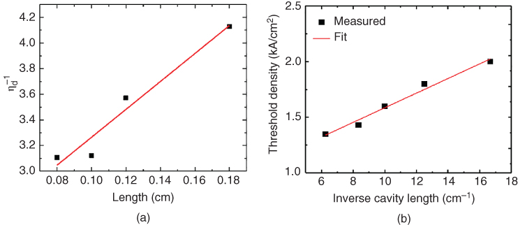
Figure 13.14 (a) Variation of inverse differential quantum efficiency with cavity length; (b) variation of threshold current density with inverse cavity length of In0.4Ga0.6N/GaN QD laser.
(Source: After T. Frost et al. [24].)
where R1 and R2 are mirror reflectivities, L is cavity length, and αi is cavity loss. The cavity loss is determined to be 8.3 cm−1 in these heterostructures. The relativity small value of the cavity loss is due to smaller free carrier absorption and substrate leakage with the In0.18Al0.82N cladding layers. Measured values of Jth are plotted against inverse cavity length in Figure 13.14(b). The differential gain dg/dn is calculated by analyzing this data with the relation [60]
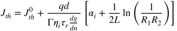
where d is the active region thickness calculated as the number of dot layers times the effective dot height, Γ is the product of the optical confinement factor simulated by the transfer matrix method (0.075) and the fill factor (0.38), τr is the measured radiative lifetime (2.5 ns), and R1 and R2 are 0.7 and 0.95, respectively. The transparency current density Jth0 and dg/dn are fitting parameters. A value of dg/dn = 9.0 × 10⁻¹⁷ cm2 is derived along with a value of Jth0 = 550 A cm−2. The large value of differential gain is comparable to those of shorter‐wavelength blue‐ and green‐emitting quantum dot lasers [ 19, 20] and is approximately five times larger than values reported for shorter‐wavelength blue‐emitting InGaN/GaN QW‐based lasers [61].
13.4.3 Small‐Signal Modulation Characteristics
An important emerging application of visible lasers is plastic‐fiber communication. For this it is important to determine the small‐signal modulation characteristics of the lasers. Important device and material characteristics can also be determined from these measurements. In the following, we describe the small‐signal modulation characteristics of red‐emitting InGaN/GaN quantum dot lasers. The laser heterostructure grown for these measurements is shown in Figure 13.15(a), which is slightly different from the one shown in Figure 13.11. Device fabrication has been described before, except that a ground–signal–ground n‐contact geometry is formed on top for high‐speed measurements. The L–I characteristics of the laser measured at room temperature with continuous wave (CW) current injection are shown in Figure 13.15(b), and the spectral output is shown in the inset. The threshold current density is 2.4 kA cm−2 and the peak emission is at 630 nm. The small‐signal modulation response of a 800 μm‐long ridge waveguide laser was measured under pulsed bias conditions (5 μs pulses, 0.5% duty cycle). The modulation response is shown in Figure 13.16(a). The indicated currents refer to the DC bias current. A 10 dBm sinusoidal signal of varying frequency (100 MHz to 3 GHz) is superimposed on the DC bias with the sweep oscillator and bias T. The measured data have been analyzed with the damped oscillator small‐signal response model
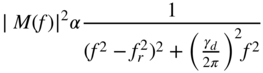
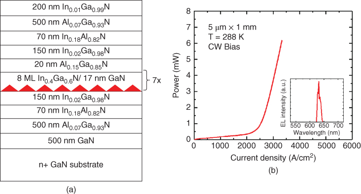
Figure 13.15 (a) Laser heterostructure used for small‐signal modulation measurements, grown by MBE; (b) light–current characteristics of a typical laser fabricated with the heterostructure shown in (a). The output spectral characteristics shown in the inset are at 2.7 kA cm−2 (1.1Jth).
(Source: After Frost et al. [22].)
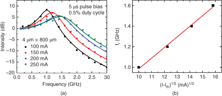
Figure 13.16 (a) Small‐signal modulation response of the In0.4Ga0.6N/GaN quantum dot laser diode (points) and analysis of the measured response curves (solid lines); (b) variation of the laser resonant frequency with the square root of the injection current above threshold. The resonant frequencies are derived from analysis of the measured data shown in (a) using the damped oscillator model.
(Source: After Frost et al. [22].)
where γd is the damping factor and fr is the resonance frequency of the response. A −3 dB modulation bandwidth of 2.4 GHz was measured at the highest DC injection current of 250 mA and the resonance frequency at this injection level is 1.6 GHz. A higher −3 dB modulation bandwidth could be measured with higher injection currents, but this was not possible due to device and facet heating. The relatively high modulation frequencies may allow for the use of these lasers in plastic‐fiber communication systems. The differential gain dg/dn is related to the resonance frequency by the relation

where vg is the photon group velocity and dact is the thickness of the active region. A value of ηi = 0.36 determined from PL measurements was used here. The confinement factor is calculated to be 0.025 for the laser heterostructure. The plot of fr vs. (I–Ith)1/2, obtained from the data of Figure 13.16(a), is shown in Figure 13.16(b). The slope of the plot is 3.3 GHz mA−1/2, from which a differential gain dg/dn = 5.3 × 10⁻¹⁷ cm2 is derived. This value is comparable to that obtained from the cavity length‐dependent steady‐state L–I measurements described earlier. Under gain compression limited modulation response in the devices studied, the damping factor γd is related to fr by the approximate relationship γd = Kfr2. The proportionality constant is the K‐factor, which is a measure of damping limited bandwidth. A plot of γd versus fr2 obtained from analysis of the data of Figure 13.16(a) with Eq. 13.7 yields K = 1.96 ns. A value of the gain compression factor ɛ = 2.87 × 1017 cm3 is then derived from the approximate relationship
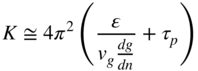
where τp is the cavity photon lifetime. This value of ɛ is comparable to those measured for In(Ga)As/GaAs quantum dot lasers [62].
13.5 Summary and Future Prospects
It is evident that self‐organized quantum dots are important for the realization of visible light emitters. They uniquely provide the dual advantages of lower polarization fields and three‐dimensional quantum confinement. Most importantly, emission at longer wavelengths, which is not possible with InGaN/GaN QWs, is made possible. In this chapter we have focused on the MBE and characteristics of quantum dots emitting at ∼630 nm (red) and their application to white converter LEDs and edge‐emitting diode lasers. While more work needs to be done, the performance of these devices is already quite good and suited for lighting, displays, communication, and other applications.
The generation of single photons on‐demand is essential for quantum cryptography, quantum metrology, and related applications. In particular, a visible single photon source is important for free‐space quantum cryptography. InGaN/GaN self‐organized quantum dots are ideally suited for this application. As we have seen, the area density of the quantum dots can be varied and, in particular, is very low in the first dot layer of a multi‐layer stack. A single photon source with optical or electrical excitation can be realized with an isolated single dot emitting in the visible range of the spectrum. We have recently reported an electrically pumped single photon source operating at room temperature [43]. The single‐dot diode heterojunction grown by PAMBE is illustrated in Figure 13.17(a). Evidence of single photon emission is seen in the Hanbury–Brown and Twiss measurement of photon pair correlation statistics. The second‐order correlation function, shown in Figure 13.17(b), exhibits a sharp minimum at zero time delay.
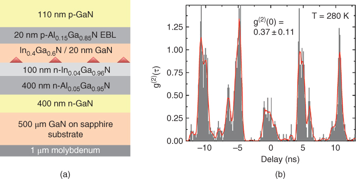
Figure 13.17 (a) Schematic of the heterostructure for electrically pumped single photon source grown on GaN‐on‐sapphire by molecular beam epitaxy. A single quantum dot is enclosed in the single photon source; (b) measurement of photon pair correlation statistics from InGaN/GaN QD device of (a) by Hanbury–Brown and Twiss measurement. The second‐order correlation is plotted against delay between the two photon counters. The solid lines represent smoothed data obtained after 5‐point moving averaging.
(Source: After Deshpande et al. [43].)
References
- 1 Nam, O.H., Ha, K.H., Kwak, J.S. et al. (2004). Phys. Status Solidi A 201: 2717.
- 2 Ohta, H., DenBaars, S.P., and Nakamura, S. (2010). J. Opt. Soc. Am. B 27: B45.
- 3 Nakamura, S., Senoh, M., Iwasa, N., and Nagahama, S. (1995). Jpn. J. Appl. Phys. 34: L797.
- 4 Narukawa, Y., Kawakami, Y., Funato, M. et al. (1997). Appl. Phys. Lett. 70: 981.
- 5 Skierbiszewski, C., Wasilewski, Z.R., Siekacz, M. et al. (2004). Appl. Phys. Lett. 86: 11114.
- 6 U. Strauβ, S. Brüninghoff, M. Schillgalies, C. Vierheilig, N. Gmeinwieser, V. Kümmler, G. Brüderl, S. Lutgen, A. Avramescu, D. Queren, D. Dini, C. Eichler, A. Lell, and U. T. Schwarz, Proc. SPIE 6894, Gallium Nitride Materials and Devices III, 6894, 689417 (2008).
- 7 Bour, D., Chua, C., Yang, Z. et al. (2009). Appl. Phys. Lett. 94: 41124.
- 8 Okamoto, K., Kashiwagi, J., Tanaka, T., and Kubota, M. (2009). Appl. Phys. Lett. 94: 71105.
- 9 Queren, D., Avramescu, A., Brüderl, G. et al. (2009). Appl. Phys. Lett. 94: 81119.
- 10 Huang, C.‐Y., Hardy, M.T., Fujito, K. et al. (2011). Appl. Phys. Lett. 99: 241115.
- 11 Skierbiszewski, C., Siekacz, M., Turski, H. et al. (2012). Appl. Phys. Express 5: 22104.
- 12 Nakamura, S., Senoh, M., Nagahama, S. et al. (1996). Appl. Phys. Lett. 69: 4056.
- 13 Enya, Y., Yoshizumi, Y., Kyono, T. et al. (2009). Appl. Phys. Express 2: 82101.
- 14 Piprek, J. (2010). Phys. Status Solidi A 207: 2217.
- 15 Sizov, D., Bhat, R., and Zah, C.‐E. (2012). J. Light. Technol. 30: 679.
- 16 Asahi, H., Kawamura, Y., and Nagai, H. (1983). J. Appl. Phys. 54: 6958.
- 17 Ikeda, M., Mori, Y., Sato, H. et al. (1985). Appl. Phys. Lett. 47: 1027.
- 18 Rennie, J., Okajima, M., Watanabe, M., and Hatakoshi, G. (1993). IEEE J. Quantum Electron. 29: 1857.
- 19 Zhang, M., Banerjee, A., Lee, C.‐S. et al. (2011). Appl. Phys. Lett. 98: 221104.
- 20 Banerjee, A., Frost, T., Stark, E., and Bhattacharya, P. (2012). Appl. Phys. Lett. 101: 41108.
- 21 Frost, T., Banerjee, A., Sun, K. et al. (2013). IEEE J. Quantum Electron. 49: 923.
- 22 Frost, T., Banerjee, A., and Bhattacharya, P. (2013). Appl. Phys. Lett. 103: 211111.
- 23 Frost, T., Banerjee, A., Jahangir, S., and Bhattacharya, P. (2014). Appl. Phys. Lett. 104: 81121.
- 24 Frost, T., Hazari, A., Aiello, A. et al. (2016). Jpn. J. Appl. Phys. 55: 32101.
- 25 Wu, Y.‐R., Lin, Y.‐Y., Huang, H.‐H., and Singh, J. (2009). J. Appl. Phys. 105: 13117.
- 26 Schulz, S. and O'Reilly, E.P. (2010). Phys. Rev. B 82: 33411.
- 27 Eliseev, P.G., Li, H., Liu, G.T. et al. (2001). IEEE J. Select. Top. Quantum Electron. 7: 135.
- 28 Fathpour, S., Mi, Z., and Bhattacharya, P. (2005). J. Phys. Appl. Phys. 38: 2103.
- 29 Bimberg, D. and Pohl, U.W. (2011). Mater. Today 14: 388.
- 30 Nakamura, S. and Chichibu, S.F. (2000). Introduction to Nitride Semiconductor Blue Lasers and Light Emitting Diodes. Boca Raton, FL: CRC Press.
- 31 Usui, A., Sunakawa, H., Sakai, A., and Yamaguchi, A.A. (1997). Jpn. J. Appl. Phys. 36: L899.
- 32 Newman, N. (1997). J. Cryst. Growth 178: 102.
- 33 Amar, J.G. and Family, F. (1995). Phys. Rev. Lett. 74: 2066.
- 34 Holmes, M.J., Choi, K., Kako, S. et al. (2014). Nano Lett. 14: 982.
- 35 Nakajima, K., Ujihara, T., Miyashita, S., and Sazaki, G. (2001). J. Appl. Phys. 89: 146.
- 36 Bayram, C. and Razeghi, M. (2009). Appl. Phys. Mater. Sci. Process. 96: 403.
- 37 Tanaka, S., Iwai, S., and Aoyagi, Y. (1996). Appl. Phys. Lett. 69: 4096.
- 38 Adelmann, C., Simon, J., Feuillet, G. et al. (2000). Appl. Phys. Lett. 76: 1570.
- 39 Tachibana, K., Someya, T., and Arakawa, Y. (2000). IEEE J. Select. Top. Quantum Electron. 6: 475.
- 40 Briot, O., Maleyre, B., and Ruffenach, S. (2003). Appl. Phys. Lett. 83: 2919.
- 41 Bhattacharya, P., Ghosh, S., and Stiff‐Roberts, A.D. (2004). Annu. Rev. Mater. Res. 34: 1.
- 42 Dehaese, O., Wallart, X., and Mollot, F. (1995). Appl. Phys. Lett. 66: 52.
- 43 Deshpande, S., Frost, T., Hazari, A., and Bhattacharya, P. (2014). Appl. Phys. Lett. 105: 141109.
- 44 Varshni, Y.P. (1967). Physica 34: 149.
- 45 Feng, S.‐W., Cheng, Y.‐C., Chung, Y.‐Y. et al. (2002). J. Appl. Phys. 92: 4441.
- 46 Ramaiah, K.S., Su, Y.K., Chang, S.J. et al. (2004). Appl. Phys. Lett. 84: 3307.
- 47 Deshpande, S., Frost, T., Yan, L. et al. (2015). Nano Lett. 15: 1647.
- 48 Wang, G., Fafard, S., Leonard, D. et al. (1994). Appl. Phys. Lett. 64: 2815.
- 49 Bhattacharya, P., Ghosh, S., Pradhan, S. et al. (2003). IEEE J. Quantum Electron. 39: 952.
- 50 Zhang, M., Bhattacharya, P., and Guo, W. (2010). Appl. Phys. Lett. 97: 11103.
- 51 Nakamura, S., Fasol, G., and Pearton, S.J. (2000). The Blue Laser Diode: The Complete Story, 2e. New York: Springer.
- 52 Sheu, J.K., Chang, S.J., Kuo, C.H. et al. (2003). IEEE Photonics Technol. Lett. 15: 18.
- 53 Huang, M. and Yang, L. (2013). IEEE Photonics Technol. Lett. 25: 1317.
- 54 Tamura, T., Setomoto, T., and Taguchi, T. (2000). J. Lumin. 87–89: 1180.
- 55 Hwang, J.‐H., Kim, Y.‐D., Kim, J.‐W. et al. (2010). Phys. Status Solidi C 7: 2157.
- 56 Qin, Z., Feng, J., Zhaohui, C. et al. (2011). J. Semicond. 32: 12002.
- 57 Yuan, C. and Luo, X. (2013). Int. J. Heat Mass Transf. 56: 206.
- 58 Jahangir, S., Pietzonka, I., Strassburg, M., and Bhattacharya, P. (2014). Appl. Phys. Lett. 105: 111117.
- 59 Castiglia, A., Feltin, E., Dorsaz, J. et al. (2008). Electron. Lett. 44: 521.
- 60 Hakki, B.W. and Paoli, T.L. (1975). J. Appl. Phys. 46: 1299.
- 61 Nakamura, S. (1997). IEEE J. Select. Top. Quantum Electron. 3: 712.
- 62 Bhattacharya, P. and Ghosh, S. (2002). Appl. Phys. Lett. 80: 3482.