8
Molecular Beam Epitaxy for Steep Switching Tunnel FETs
Salim El Kazzi
IMEC, Leuven, 3001, Belgium
8.1 Introduction
The advent of 5G communications and the convergence with the Internet of Things (IoT) require next‐generation energy‐efficient devices which can integrate into our daily life. From autonomous cars to drones, entertainment, defense technologies, health services and low‐power pervasive radio frequency (RF) communication, technology enablers incorporating large‐scale‐integration chips with extremely low power consumption are in huge need [1]. At the transistor level, one of the main requirements is to achieve very steep devices operating at supply voltages (Vdd) less than 0.5 V. Therefore, tunneling field effect transistors (TFETs) are being explored as the most promising devices which can answer this demand and help in reducing power consumption and boosting performance [2,3].
In this chapter, we try to show the importance of molecular beam epitaxy (MBE) as an ideal technique for making next‐generation low‐power tunneling devices. We start with a brief introduction of the TFET working principle and its main advantage over the traditional metal–oxide–semiconductor field effect transistor (MOSFET). Then, we show how III–V properties and their capability to offer different band alignments make them promising alternatives to Si in TFETs. After showing an example of an ideal MBE production cluster for complementary metal–oxide–semiconductor (CMOS) technology, we discuss the main challenges encountered during the epitaxial growth of III–V tunneling devices and how MBE is helping in solving them.
8.2 TFET Working Principle
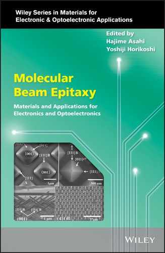
The basic working principle of a TFET, especially its switching mechanism, is compared with that of a traditional MOSFET in Figure 8.1. Unlike MOSFETs, where the source and drain have the same doping polarity (i.e. n+/i/n+ for n‐MOS or p+/i/p+ for p‐MOS), TFETs operate like a reversed p–i–n diode which is gate controlled (p+/i/n+ for n‐TFET and n+/i/p+ for p‐TFET). Here, we take the example of an n‐(MOS)TFET configuration with a gate stack over the intrinsic region.
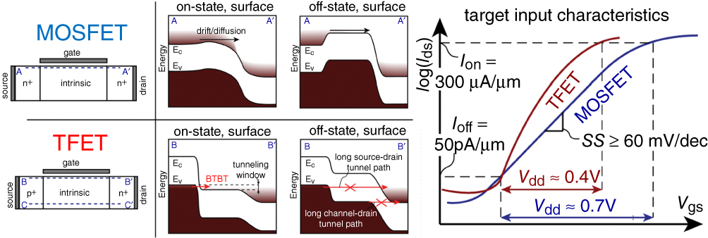
Figure 8.1 A comparison of the basic working principle of a MOSFET and a TFET reproduced by permission from [4]. The graph shows MOSFET transfer characteristics with SS < 60 mV dec−1, and target characteristics of an optimized TFET operating at smaller Vdd than the MOSFET.
For MOSFETs, the high gate voltage in the on‐state regime reduces the band energies of the channel region. This allows the flow of electrons from the conduction band (CB) of the n+ source region to the CB of the n+ drain region through the channel CB. In the off‐state regime, the potential barrier imposed by the channel prevents the flow of the majority of the CB source electrons. However, the very high‐energy electrons still succeed in being injected into the channel because of thermionic emission. This phenomenon is the core reason for the MOSFET sub‐threshold swing theoretical limit SS = ln(10)kBT/q = 60 mV dec−1 at room temperature, where T is the temperature, kB is the Boltzmann constant, and q is the electron charge.
For TFETs, the behavior is different. In the on‐state regime, the high gate voltage suppresses the energy bands of the channel. But this time, the electrons reach the CB of the channel from the electron valence band (VB) of the p+ source region through an energy filtering mechanism by band‐to‐band tunneling (BTBT). In the off‐state, the tunneling path of these electrons becomes much longer (Figure 8.1). Compared to a MOSFET, the high‐energy carriers from the Fermi–Dirac tail are now eliminated by the bandgap in the p‐type source and thermionic emission is therefore absent. It is this steep change from short to long tunnel paths which allows TFETs to operate with SS < 60 mv dec−1 at a potentially smaller Vdd and thus lower power than MOSFETs (see graph in Figure 8.1).
8.3 III–V Heterostructure for TFETs
The graph in Figure 8.1 clearly highlights the benefit of TFETs over MOSFETs for low‐power applications. However, it points out that in order for TFET to compete with MOSFET, Ion should be in the range of 300 µA µm−1 for Vdd at 0.4 V, combined with a low SS over several decades of current while maintaining a low Ioff of ∼50 pA µm−1. With the target to find ideal materials to boost Ion in TFETs, Smets and Renard [4] compared the BTBT generation rate (G) as a function of the electric field (E) for different active‐layer materials of Esaki tunneling diodes [Figure 8.2(a)].

Figure 8.2 (a) A simulated comparison of generation rate vs. electric field for different active‐layer material Esaki diodes [4]. (b) Quantum mechanical simulated transfer characteristics for an In0.53Ga0.47As homostructure TFET and a GaAs0.5Sb0.5/In0.53Ga0.47As heterostructure TFET [5]. Both figures are reproduced by permission.
They demonstrated how III–V single‐material generation rates exceed the group IV ones for lower electric fields, basically due to the lower electron mass of the III–V compound and the switch from an indirect to a direct bandgap. Nevertheless, the use of a small bandgap combined with a low effective mass also facilitates both ambipolar and direct source–drain tunneling, which can induce high Ioff. This can be solved by the use of III–V heterostructure configurations, where different materials are used in one system. This actually allows us to have a large bandgap at the channel–drain junction, for example, and solve the problem of any Ioff degradation. Verreck and Webster [5] showed how the use of heterostructure TFET would help in solving this problem by comparing simulated I–V characteristics of InGaAs homostructure and heterostructure staggered gap (SG) InGaAs/GaAsSb TFETs [Figure 8.2(b)]. It is clear how the heterostructure TFET exhibits better SS than the homostructure one. Furthermore, the difference in the band alignment of the SG allows a decrease in the effective bandgap, which means a smaller electron tunneling length and thus a higher Ion in TFETs. This has also been expected for the broken gap (BG) configurations, which would further decrease the tunneling length and improve drive currents [5].
A summary of the reported TFETs with different configurations is compared with the state‐of‐the‐art MOSFET (modified from ref. [6]). Here we would like to mention that even if other promising TFETs are made using other techniques {e.g. exfoliation of 2D dichalcogenide materials [7] or carbon nanotubes (CNTs) [8]}, we only focus in our study on III–V TFEETs which are directly epitaxially grown on commercial substrates (see Figure 8.3).

Figure 8.3 Experimental transfer characteristics in the literature 7–24 of nTFET and pTFET with SS < 70 mV dec−1. This figure is an updated version of Figure 2 of Lu and Seabaugh [6].
We first notice that TFETs with a III–V heterostructure system lead to much better characteristics than a single‐material TFET, where a trade‐off between Ion and Ioff is observed (i.e. either a high Ion with a high Ioff or a decent Ioff but a low Ion). However, it is clear that none of these devices meet the target input characteristics defined in Figure 8.1, due to many traditional device fabrication problems (channel growth, gate stack, contacts, etc.) [ 3, 4]. In the following section, we focus on the interface defects [like trap‐assisted tunneling (TAT) and Shockley–Read–Hall (SRH)] which are found at the tunnel junction of a TFET and play a unique role in device performance.
8.4 MBE for Beyond CMOS Technologies
In order to make III–V TFETs operate with the desired characteristics, the different material components constituting these devices – as well as the interfaces between them – should be at their best. One would need to carefully choose the exact growth machines for the different deposition steps. An example of a suitable machine to grow TFETs is the RIBER 200‐mm MBE production cluster installed at IMEC (Belgium) and depicted in detail in Figure 8.4. This cluster is used to study different kinds of FET devices and consists of one III–V MBE machine, one passivation chamber, and one oxide deposition machine. One of the main advantages of this cluster is the connection of the three machines under ultra‐high vacuum (UHV), which protects for instance the III–V channel surface from being oxidized before the gate stack deposition. This has been shown to be a critical step for lowering defects at the channel/gate interface (Dit, interface traps, etc.) [25].

Figure 8.4 The 200‐mm RIBER cluster installed at IMEC consisting of three MBE machines and used for the large‐area growth of novel materials for beyond CMOS technology.
Many studies in the literature on passivation and gate stack deposition on group IV and III–V surfaces (like GaAs, GaSb, InGaAs, etc.) using MBE technique can be found [26–28], and all these studies are of crucial importance for FET fabrication. Since our chapter highlights the MBE advantage for tunnel devices, we keep our discussion to III–V epitaxial growth of the tunneling active area, which is the main difference between TFET and other FET devices.
8.5 Doping
As mentioned, TAT, interface defects, phonon‐assisted tunneling, and band tails have all been shown to contribute to TFET performance [5]. Since doping, which is a point defect, can be the main source in all this, but also affects the system band configuration [29], studies on III–V doping and its effects on structural and tunneling properties are mandatory. As an example, we present in Figure 8.5 the effects of Si (Be) doping on the InGaAs (GaAsSb) layer grown on (001) InP in our III–V MBE tool [30]. It can be seen from the microscope images that the Si doping at high concentrations (>2e19 cm−3) leads to the deterioration of the InGaAs crystalline quality. Also, doping polarity deviation is observed at high concentrations due to the amphoteric nature of Si in InGaAs [31]. For the Be case, no clear surface degradation is observed at high doping concentrations. However, a p‐type doping saturation starts to be observed when the hole concentration reaches the range of 1e19 cm−2 (nearly 820 °C for cell temperature).

Figure 8.5 Carrier concentrations and electron mobility measured by Hall of Si‐doped (a) and Be‐doped (b) InGaAs grown on (001) Si InP as a function of Si and Be cell temperatures, respectively. The optical microscope images are used to assess layer quality.
Since our idea is to understand the growth influence on BTBT and separate it from other challenges (like gate stack or contacting), we have already proposed an easy BTBT measurement method using highly doped Esaki tunneling diodes to have accurate TFET predictions [32]. Using the above results, Esaki tunneling diodes are grown by the EPIPHY group (IEMN‐Lille) [30] with maximum Si n‐type doping of 1e19 cm−3 for InGaAs to avoid any III–V material degradation and carbon (C) instead of Be for p+ doping due to its low diffusivity and ability to achieve very high p‐type doping in III–V materials [33].
The SIMS dopant profiles of the different Esaki diode heterostructures fabricated using either Be or C‐doped GaAs0.5Sb0.5 are shown in Figure 8.6, along with the corresponding I–V characteristics. Si, Be, and C (even at high concentrations, ED3) exhibit slopes less than 10 nm dec−1, which is considered a rough guide line to allow TFET operation with SS ≪ 60 mV dec−1 [34]. This highlights the MBE advantage as a suitable doping control technique, which allows high doping concentrations with steep gradients. One can also see a similar J–V behavior by using either Be or C as p+ dopant in GaAsSb (ED1 and ED2). The peak current in ED3 shows a higher current value with a slight shift of the supply voltage. This is due to the higher doping concentration, which increases the band overlaps and reduces the tunneling length. This will also result in a decrease of the peak‐to‐valley ratio (PVCR) values with the doping concentration (ED1 = 13; ED2 = 13; ED3 = 5). The lower PVCR is caused by band tails due to random dopant fluctuations or extra defect states. Alternatively, it may also be due to a higher hole quasi‐Fermi level degeneracy. Ongoing simulation and experimental works, for example on quantifying TATs [35] and understanding Urbach tails [36] at different doping levels, aim to reveal the role of doping on BTBT behavior and thus provide deeper learning on experimental TFETs.
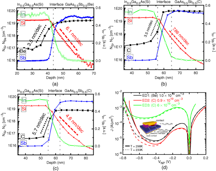
Figure 8.6 SIMS analyses of three different Esaki diodes: (a) ED1, (b) ED2, and (c) ED3 with nearly the same n+ Si doping and different p+ doping. For p+ GaAs0.5Sb0.5, ED1 is 1e19 cm−2 for Be doping and ED2 (ED3) are 1e19 cm−2 (6e19 cm−2) for C doping. (d) J–V characteristics of the three diodes [30].
8.6 Tunneling Interface Engineering
Other sources of interface defects at the tunneling region are interface roughness and stoichiometry engineering during epitaxial growth of this interface. Studies have already reported the importance of growing by MBE sharp and defect‐free heterointerfaces for many electronic or photonic devices [37–40]. For TFETs, Zhu et al. [41] compared III–V TFET grown by MBE with different tunneling interface stoichiometry, as shown in Figure 8.7(a). They demonstrated that an InAs‐like interface is essential at the In0.7Ga0.3As/GaAs0.35Sb0.65 source channel tunneling region. This confines strain between the layers, inducing sharp interfaces with much better TFET characteristics compared to when a GaAs‐like interface is used. At a later stage, they proved that a defective interface would change the bandgap configuration of the system from a staggered bandgap to a broken bandgap [43].
Figure 8.7 (a) Cross‐section TEM images of In0.7Ga0.3As/GaAs0.35 Sb0.65 TFETs grown with GaAs‐like and InAs‐like interfaces along with their corresponding I–V [41]. (b) InAs/GaSb TFET fabricated by Rajamohanan et al. [42] showing a GaAsSb amorphous layer at the tunneling region, which is the region of Ioff degradation..
Source: The figures are reproduced from [ 41, 43] with the permission of AIP Publishing
Alternatively, Rajamohanan et al. [42] fabricated broken‐gap p‐type InAs/GaSb TFETs [Figure 8.7(b)]. From the IDS–VGS characteristics of the device, they noticed high Ioff of 1 µA µm−1 at 300 K, which reduces substantially at 150 K and Ion/Ioff improves to 104. They related the Ioff degradation to the GaAsSb amorphous layer at the tunneling InAs/GaSb region and concluded that optimized MBE growth conditions will help in reducing tunneling defects, which would translate into better TFET performance.
In our group we have investigated tunneling interface engineering for both the staggered‐gap n+ (50 nm)/p+ (600 nm) In0.53Ga0.47As/GaAs0.49Sb0.51 [30] and broken‐gap InAs/GaSb systems [44] [Figures 8.8(a–c) and (d–e), respectively]. For the SG system, we have first studied the right growth conditions to grow GaAsSb and InGaAs separately at the same growth temperature [45]. Proper monitoring of the MBE shutter sequence was then used to grow InGaAs/GaAsSb Esaki diodes [30] with different interface stoichiometry [see e.g. the GaAs‐like interface in Figure 8.8(a)]. High‐angle annular dark field (HAADF)‐HR‐STEM was used to carefully probe the interface stoichiometry of samples with different interface engineering, as shown in the example of Figure 8.8(b). The diodes fabricated with different interface stoichiometry in the SG showed similar J–V behavior [Figure 8.8(c)]. We believe that since GaAsSb and InGaAs are nearly perfectly matched and grown pseudomorphically on InP, whatever the interface stoichiometry is, the interface can be kept strained and thus no relaxation or dislocations are introduced. However, this behavior was different for the BG system, where InAs and GaSb have a small 0.6% mismatch: as can be see from the I–V characteristics in Figure 8.8(e), a higher valley current is observed for the GaAs‐like interface with nearly no negative differential resistance (NDR). On the other hand, a clear NDR is observed for the InSb‐like case with a peak current reaching 8 µA µm−1. The difference in the device behavior is linked to material degradation for the GaAs‐like interface case [see Figure 8.8(d)], which is related to strain relaxation by 60° misfit dislocations (MDs) at the InAs/GaSb tunneling interface [44].
![Graph of layer vs. shutter displaying horizontal lines labeled InGaAs, Ga, As, and GaAsSb intersected by vertical lines labeled As, Ga, Sb, and In. At the left are circles labeled As, Ga, and In.; HAADF-HR-STEM with a horizontal line intersected by 3 slightly diagonal bars labeled A, B, and C (top) and graphs of counts x [104] vs. distance displaying waveforms with peaks pointed by arrows for Ga, As, etc. (bottom).; Graph of current density [A/μm2] vs. Vnp [V] displaying almost coinciding descending-ascending curves for GaAs-like, InSb-like, and InAs-like. SRH and BTBT are indicated alongside the curves.; Cross-section HAADF-HR-STEM of InAs/GaSb diodes grown with InSb-like and GaAs-like interfaces (top) and graphs of counts - [104] vs. distance [nm] displaying waveforms with labels Ga, Sb, As, and In (bottom).; Graph of current density [A/μm2] vs. Vnp [V] displaying descending-ascending curves for InSb-like interface and GaAs-like interface.](http://images-20200215.ebookreading.net/2/1/1/9781119355014/9781119355014__molecular-beam-epitaxy__9781119355014__images__c08f008.jpg)
Figure 8.8 (a) An example of the MBE shutter sequence to achieve a GaAs‐like interface as shown in the HAADF‐HR‐STEM of (b) [29]. (c) J–V characteristics of In0.53Ga0.47As/GaAs0.49Sb0.51 diodes grown with different interface stoichiometry [30]. (d) Cross‐section HAADF‐HR‐STEM of InAs/GaSb diodes grown with InSb‐like and GaAs‐like interfaces along with (e) their corresponding J–V characteristics [44].
8.7 MBE for III–V TFET Integration
Until now, we have discussed the problems which can be encountered during growth of the III–V active area without handling the challenges coming from the substrates. To reach industry, TFETs would need to be integrated on commercial substrates (like Si or GaAs), which usually have a large lattice mismatch with the device active area. Furthermore, nanowire (NW)‐based devices are believed to be the ideal architecture for TFET characteristics [46]. Hence, two main routes are being investigated in order to achieve III–V NW TFETs on commercial substrates. Here, we will focus on how MBE is helping in both approaches.
- The first route is a ‘top‐down’ approach, depicted in the left part of Figure 8.9. It consists of growing the III–V heterostructures on commercial blanket substrates, followed by careful III–V NW etching to reach very narrow NW diameters (sub‐10 nm) [52]. The different studies on the MBE growth of tunneling diodes and TFETs on blanket substrates which are relevant for this route are also presented in Figure 8.9. The main epitaxial challenge is to decrease the defect density in the active area caused by the mismatch with the substrate. For instance, S. Datta's group from Pennsylvania State University [Figure 8.9(a)] used MBE to mitigate the detrimental defects by bending the vertically propagating defects coming from 60° MDs using compositionally graded layers [ 41, 43]. Thomas et al. [51] used buffer layers to grow InGaAs tunneling diodes on Si and reported nearly similar electrical results when compared to the lattice‐matched InP growth, highlighting the high III–V on Si crystal quality [Figure 8.9(b)]. In the same context, Liu et al. [47] and Bhatnagar et al. [50] both grew BG InAsGaSb Esaki diodes on GaAs [Figure 8.9(c)] and Si substrates [Figure 8.9(d)], respectively. By using 90° interfacial MDs at the III‐Sb buffer layer/substrate [the interface misfit (IMF) technique], the mismatch is revealed instantly at the first monolayer of growth. Both groups report severe device degradation when mismatched substrates are used, due to the high threading dislocation (TD) density. Since the IMF method already showed very low TD densities (<5×105 cm−2) with MBE [53] due to the convenient energy formation of 90° MDs, especially when Sb‐rich substrate surfaces are used [54], this technique can offer an important promise for tunneling device integration on (001) Si substrates.
- The second route is a ‘bottom‐up’ approach presented on the right‐side line of Figure 8.9. Here the idea is to grow ordered III–V NW directly on commercial substrates. With this technique, pattern substrates are used to predefine the location of the NW growth and thus selective area epitaxy (SAE) is required. Usually with MBE, catalyst‐assisted growth (Ga [55], Au [56], etc.) is used to induce selective III–V NW growth on (111) Si substrates. Even if NW tunneling devices were fabricated by transferring NWs grown by catalyst‐assisted MBE [57], this method is too complex and difficult to be implemented, mainly due to contamination problems of the catalyst. Recently, the MBE team of the Technical University of Munich (TUM) successfully demonstrated catalyst‐free SAE growth of InxGa1−xAs NW by MBE [Figure 8.9(e–g)] on pattern SiO2/Si templates by carefully tuning the growth conditions and forbidding any deposition on the surface mask [48]. Using C‐AFM, they confirmed interband tunneling of MBE‐grown In(Ga)As NW diodes directly integrated on p‐Si substrate [Figure 8.9(h)] [49]. Another interesting approach for SAE growth of III–V TFET in pattern (001) substrates is the use of atomic hydrogen flux during the epitaxy to influence group III desorption [58] and assure the absence of growth on the surface mask [59].
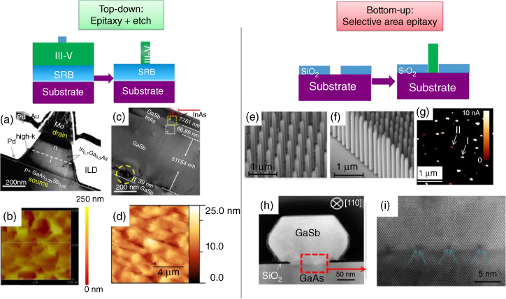
Figure 8.9 Overview of the different works found in the literature for III–V TFET integration on commercial substrates using either ‘top‐down’ or ‘bottom‐up’ approaches. The details of each work are in the text..
Source: (a, c, g, e, f) are reproduced from [ 41 47– 49] with the permission of AIP Publishing. (b) From [50] with the permission of the American Vacuum Society. (d) From [51] with the permission of IEEE
With this technique, an InAs/Al0.5Ga0.5Sb vertical TFET on (001) GaAs was fabricated [60] with a large Ion of 433 µA µm−1 at VDS = VGS = 0.5 V and SS of 71 mV dec−1 at 77 K. Later, the same group reported the first dislocation‐free GaSb growth on large lattice‐mismatched GaAs [Figure 8.9(i, j)] [61], which interestingly opens the path for III–V NW TFET integration into (001) commercial substrates.
8.8 Conclusions and Perspectives
In summary, this chapter presents an overview of the main works done with MBE for the new era of TFET devices. After introducing the basic working principle of TFETs and highlighting their advantage on MOSFETs, we have shown how these new devices are still lacking behind their expected performance. By giving an example of an ideal MBE cluster to investigate different TFET material problems, we have focused our discussion on the epitaxial growth of the tunneling active area, which is the unique property of TFETs. First, we demonstrated that a unique understanding of the doping effect on both the structural and electrical results is of high importance to understand TFET performance. Then, we showed how careful MBE growth is helping to get defect‐free and high‐quality tunneling interface layers. Finally, we proved that MBE is being used in both ‘top‐down’ and ‘bottom‐up’ approaches to fabricate tunnel devices where the main challenges and solutions are addressed for the different techniques.
It is clear from this overview that many challenges need to be overcome in order to integrate III–V TFETs on large‐area commercial substrates. However, we highlight in this work the main challenges that need to be addressed and how one can work to solve them using the MBE technique. Finally, even though we have tackled in our work the importance of III–V TFETs, we believe that MBE will further offer new insights and solutions for the next generation of 2D materials, pushing by this the CMOS technology roadmap through MX2 TFET devices onto Si substrates.
Acknowledgments
The author would like to thank all the IMEC TFET team members, especially Devin Verreck, Quentin Smets, and C. Merckling, for fruitful discussions and support of this overview.
References
- 1 A. Steegen, Symposium on VLSI Circuits, C170–171 (2015).
- 2 Ionescu, A.M. and Riel, H. (2011). Nat. Rev. 479: 329.
- 3 Núñez, J. and Avedillo, M.J. (2016). IEEE Trans. Electron Devices 63: 5012.
- 4 Smets, Q. and Renard, C. (2016). Calibration of Models for III–V TFET Performance Prediction. Belgium: KU Leuven.
- 5 D. Verreck and J. Webster (eds), Wiley Encyclopedia of Electrical and Electronics Engineering 2016 Wiley, New York.
- 6 Lu, H. and Seabaugh, A. (2014). IEEE J. Electron Device Soc. 2: 44–49.
- 7 Sarkar, D., Xie, X., Liu, W. et al. (2015). Nature 526 (7571): 91–95.
- 8 Lu, Y., Bangsaruntip, S., Wang, X. et al. (2006). J. Am. Chem. Soc. 128 (11): 3518–3519.
- 9 K. Jeon, W. Y. Loh, P. Patel, C. Y. Kang, J. Oh, A. Bowonder, C. Park, C. S. Park, C. Smith, P. Majhi, H. H. Tseng, R. Jammy, T. J. K. Liu, and C. Hu. Symposium on VLSI Technology, pp. 121–122 (2010)
- 10 Gandhi, R., Chen, Z., Singh, N. et al. (2011). IEEE Electron Device Lett. 32 (11): 1504–1506.
- 11 Morita, Y., Mori, T., Migita, S. et al. (2014). IEEE Electron Device Lett. 35: 792–794.
- 12 A. Villalon, C. Le Royer, M. Cassé, D. Cooper, B. Prévitali, C. Tabone, J.‐M. Hartmann, P. Perreau, P. Rivallin, J.‐F. Damlencourt, et al. Symposium on VLSI Technology (VLSIT) IEEE, 2012, pp 49–50.
- 13 Leonelli, D., Vandooren, A., Rooyackers, R. et al. (2010). Jpn. J. Appl. Phys. 49 (4S): 04DC10.
- 14 K. Tomioka, M. Yoshimura, and T. Fukui. Symposium on VLSI Technology (VLSIT) EEE, pp 47–48. (2012)
- 15 Dewey, G., Chu‐Kung, B., Boardman, J. et al. (2011). Int. Electron Device Meet. 3: 33.6.1–33.6.4.
- 16 S. H. Kim, H. Kam, C. Hu, and T. J. K. Liu. Symposium on VLSI Technology (VLSIT) EEE, pp 178–179. (2009)
- 17 Krishnamohan, T., Kim, D., Raghunathan, S., and Saraswat, K. (2008). Proceedings of IEEE International Electron Devices Meeting, 1–3.
- 18 Alian, A., Franco, J., Vandooren, A. et al. (2015). Proceedings of IEEE International Electron Devices Meeting, 31.7.1–31.7.4.
- 19 Huang, Q., Huang, R., Wu, C. et al. (2014). Proceedings of IEEE International Electron Devices Meeting, 13.3.1–13.3.4.
- 20 Appenzeller, J., Lin, Y.‐M., Knoch, J., and Avouris, P. (2004). Phys. Rev. Lett. 93: 196805.
- 21 Ganjipour, B., Wallentin, J., Borgstrom, M.T. et al. (2012). ACS Nano 6 (4): 3109–3113.
- 22 Gandhi, R., Chen, Z., Singh, N. et al. (2011). IEEE Electron Device Lett. 32 (4): 437–439.
- 23 Huang, Q., Huang, R., Zhan, Z. et al. (2012). Proceedings of IEEE International Electron Devices Meeting, 8.5.1–8.5.4.
- 24 Memisevic, E., Svensson, J., Hellenbrand, M. et al. (2016). Proceedings of IEEE International Electron Devices Meeting, 19.1.1–19.1.4.
- 25 Scarrozza, M., Pourtois, G., Houssa, M. et al. (2009). Surf. Sci. 603: 203.
- 26 Merckling, C., Chang, Y.C., Lu, C.Y. et al. (2011). Surf. Sci. 605: 1778–1783.
- 27 Merckling, C., Sun, X., Alian, A. et al. (2011). J. Appl. Phys. 109: 073719.
- 28 Chu, L.K., Merckling, C., Alian, A. et al. (2011). Appl. Phys. Lett. 99: 042908.
- 29 Smets, Q., Verhulst, A.S., El Kazzi, S. et al. (2015). Appl. Phys. Lett. 107: 072101.
- 30 El Kazzi, S., Alireza, A., Bordallo, C.C.M. et al. (2016). ECS Trans. 72: 73.
- 31 Fedoryshyn, Y., Beck, M., Kaspar, P., and Jaeckel, H. (2010). J. Appl. Phys. 107: 093710.
- 32 Smets, Q., Verreck, D., Verhulst, A.S. et al. (2014). J. Appl. Phys. 115: 184503.
- 33 Yarekha, D.A., Godey, S., Wallart, X. et al. (2007). J. Cryst. Growth 301–302: 217–220.
- 34 M. Noguchi, S. Kim, M. Yokoyama, S. Ji, O. Ichikawa, T. Osada, M. Hata, M. Takenaka and S. Takagi (2013). Proceedings of IEEE International Electron Devices Meeting, 28.1.1–28.1.4.
- 35 Smets, Q., Verhulst, A.S., Simoen, E. et al. (2017). IEEE Trans. Electron Device 64: 3622–3626.
- 36 Memisevic, E., Lind, E., Hellenbrand, M. et al. (2017). IEEE Electron Device Lett. 38: 1661–1664.
- 37 Tuttle, G., Kroemer, H., and English, J.H. (1990). J. Appl. Phys. 67: 3032.
- 38 Zaknoune, M., Mairiaux, E., Roelens, Y. et al. (2012). IEEE Electron Device Lett. 33 (10): 1381.
- 39 Greiling, P. (1997). J. Cryst. Growth 175&176: 8.
- 40 Brandstetter, M., Kainz, M.A., Zederbauer, T. et al. (2016). Appl. Phys. Lett. 108: 011109.
- 41 Zhu, Y., Jain, N., Vijayaraghavan, S. et al. (2012). J. Appl. Phys. 112: 024306.
- 42 Rajamohanan, B., Mohata, D., Zhu, Y. et al. (2014). J. Appl. Phys. 115: 044502.
- 43 Zhu, Y., Jain, N., Vijayaraghavan, S. et al. (2012). J. Appl. Phys. 112: 094312.
- 44 El Kazzi, S., Alian, A., Hsu, B. et al. (2017). J. Cryst. Growth https://doi.org/10.1016/j.jcrysgro.2017.12.035.
- 45 El Kazzi, S., Smets, Q., Ezzedini, M. et al. (2015). J. Cryst. Growth 424: 62.
- 46 Knoch, J., Mantl, S., and Appenzeller, J. (2007). Solid‐State Electron. 51: 572–578.
- 47 Liu, J.S., Clavel, M.B., Pandey, R. et al. (2016). J. Appl. Phys. 119: 244308.
- 48 Hertenberger, S., Rudolph, D., Bichler, M. et al. (2010). J. Appl. Phys. 108: 114316.
- 49 Yang, T., Hertenberger, S., Morkotter, S. et al. (2012). Appl. Phys. Lett. 101: 233102.
- 50 Bhatnagar, K., Caro, M.P., Rojas‐Ramirez, J.S. et al. (2015). J. Vac. Sci. Technol. B 33: 062203.
- 51 Thomas, P., Filmer, M., Gaur, A. et al. (2015). IEEE Trans. Electron Device 62: 2450.
- 52 Lu, W., Zhao, X., Choi, D. et al. (2017). IEEE Electron Device Lett. 38: 548.
- 53 Huang, S.H., Balakrishnan, G., Khoshakhlagh, A. et al. (2006). Appl. Phys. Lett. 88: 131911.
- 54 Wang, Y., Ruterana, P., Chen, J. et al. (2013). ACS Appl. Mater. Interfaces 5 (9760).
- 55 Dropiewski, K., Tokranov, V., Yakimov, M. et al. (2017). J. Vac. Sci. Technol. B 35: 02B.
- 56 Thelander, C., Caroff, P., Plissard, S., and Dick, K.A. (2012). Appl. Phys. Lett. 100: 232105.
- 57 Nadar, S., Rolland, C., Lampin, J.‐F. et al. (2015). Nano Res. 8: 980.
- 58 Sugaya, T., Okada, Y., and Kawabe, M. (1992). Jpn. J. Appl. Phys. 31: L713.
- 59 Desplanque, L., Fahed, M., Han, X. et al. (2014). Nanotechnology 25: 465302.
- 60 Chinni, V.K., Zaknoune, M., Coinon, C. et al. (2016). IEEE J. Electron Device Soc. 5: 44.
- 61 Fahed, M., Desplanque, L., Troadec, D. et al. (2017). J. Cryst. Growth 477: 45.