12
MBE of III‐Nitride Heterostructures for Optoelectronic Devices
C. Skierbiszewski1,2, G. Muziol1, H. Turski1, M. Siekacz1, K. Nowakowski‐Szkudlarek1, A. Feduniewicz‐Żmuda1, P. Wolny1 and M. Sawicka1,2
1Institute of High Pressure Physics, Polish Academy of Sciences, Sokolowska 29/37, 01‐142 Warsaw, Poland
2TopGaN Ltd., Sokolowska 29/37, 01‐142 Warsaw, Poland
12.1 Introduction
Gallium nitride (GaN) is considered to be the semiconductor of the twenty‐first century. A direct bandgap that covers the full visible spectral range, starting from 0.7 eV for InN, through 3.4 eV for GaN and 6.0 eV for AlN, makes it an ideal candidate for application in optoelectronics [1]. The initial material quality challenges related to lack of native GaN substrates and difficulties in p‐type doping have not discouraged interest in nitrides. In fact, they triggered even more intensive research to understand and overcome the factors limiting progress [2,3]. The first demonstration of a blue‐violet laser diode (LD) by Shuji Nakamura was done at Nichia Co. in 1996 [4,5], and since then numerous technology advancements and improvements in structure design have been reported [6]. Nowadays, nitride‐based light‐emitting diodes (LEDs) and LDs are widely used in general lighting, projection and displays, data storage, sensors, high‐resolution printing, and light‐based communication systems, thus having unquestionably a great impact on human life.
Two technologies are commonly used to fabricate the epitaxial structures of nitride‐based optoelectronic devices: metal‐organic vapor phase epitaxy (MOVPE), which is used for most commercial applications, and molecular beam epitaxy (MBE) technology, which seems to be rather limited to the research area. However, there might be some applications limited to MBE, as material grown with this technique does not suffer p‐type passivation or InGaN decomposition. The first MBE‐grown blue‐violet LDs were demonstrated in 2004 by ammonia‐MBE [7,8] and later the same year by plasma‐assisted MBE (PAMBE) [9]. However, the technological issues related to very high ammonia flow needed for the stabilization of the growth surface at high growth temperatures can be considered to be a drawback when compared to PAMBE [10]. The good material quality in PAMBE is achieved under group III‐rich conditions, in spite of the relatively low growth temperatures, 650–750 °C [11]. Both theoretical [12,13] and experimental [14] efforts were needed to understand and control the growth kinetics for such metal‐rich conditions. The refinement of the PAMBE growth conditions on GaN/sapphire MOVPE templates allowed the demonstration of promising LED devices [15]. The introduction of high‐quality GaN substrates led to truly significant improvements in the optical quality of PAMBE‐grown structures, resulting in room‐temperature high‐power pulsed and continues wave (CW) blue‐violet LDs [ 9,16] as well as GaN/AlGaN heterostructures with record high mobility of two‐dimensional electron gas [17,18].
In this chapter we report on the scientific and technological contribution to nitride device growth made by PAMBE on c‐plane (0001) GaN and concentrate on the achievements in the area of edge‐emitting nitride LDs. Since the first demonstration of PAMBE‐grown blue‐violet LDs operating at λ = 411 nm [9], the emission wavelength has evolved through true‐blue (λ = 450 nm [19]) up to cyan (λ = 482–489 nm [20]). Green optically pumped lasers for 501 nm were demonstrated [21]. Additionally, ultraviolet semipolar ![]() LDs emitting at λ = 388 nm were fabricated on bulk ammono‐thermal GaN substrates [22,23]. Simultaneous with the increase in emission wavelength, new LD structure concepts were developed and proposed. Incorporation of high‐quality InGaN waveguides allowed us to improve the optical mode confinement and eliminate light leakage to the substrate. Material quality optimizations, along with the use of ultra‐low dislocation density GaN substrates, led to the demonstration of (i) high‐power blue LDs, (ii) long‐wavelength LDs, and (iii) long‐lived blue LDs with a lifetime of 100 000 hours. Recently, the application of a tunnel junction (TJ) in the LD structure has been realized, opening up new possibilities for device architecture and end‐user applications.
LDs emitting at λ = 388 nm were fabricated on bulk ammono‐thermal GaN substrates [22,23]. Simultaneous with the increase in emission wavelength, new LD structure concepts were developed and proposed. Incorporation of high‐quality InGaN waveguides allowed us to improve the optical mode confinement and eliminate light leakage to the substrate. Material quality optimizations, along with the use of ultra‐low dislocation density GaN substrates, led to the demonstration of (i) high‐power blue LDs, (ii) long‐wavelength LDs, and (iii) long‐lived blue LDs with a lifetime of 100 000 hours. Recently, the application of a tunnel junction (TJ) in the LD structure has been realized, opening up new possibilities for device architecture and end‐user applications.
12.2 Low‐Temperature Growth of Nitrides by PAMBE
The main difficulty in GaN growth by PAMBE is the fact that for optimum growth temperature (roughly half of the melting point of GaN – around 1300 K), a high nitrogen overpressure (60 bars for N2 molecules) is required to prevent GaN decomposition [24,25]. For more chemically active nitrogen precursors, like ammonia, the situation is better, but still an overpressure in the range of 0.1–2 bar must be used – like is realized in MOVPE. Such high overpressures are not compatible with the MBE technology, which relies on high vacuum conditions for the delivery of atoms from the effusion cells to the growing layer. This situation is even more difficult for InGaN growth, for which much higher nitrogen overpressure is required to stabilize the surface against decomposition. In our opinion this is the main reason why MBE using “classical” growth conditions (i.e. group V‐rich growth) cannot compete with MOVPE in the field of optoelectronic devices.
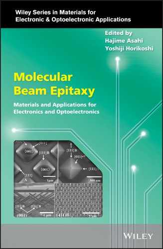
The major breakthrough in the understanding of PAMBE epitaxy came with the finding that it is possible to grow smooth layers at temperatures much lower than expected from the considerations outlined above using Ga‐rich conditions [ 11, 14, 1826–30]. Furthermore, a lower growth temperature reduces the nitrogen overpressure required for high‐quality epitaxy by orders of magnitude. However, metal‐excess growth conditions were prone to the formation of Ga droplets on the GaN surface, and high‐quality material was mainly formed in the regions between the droplets. Further study of the Ga surfactant effect revealed that this problem could be avoided, provided that the Ga‐to‐N flux ratio was maintained in a very narrow range of values: low enough to be just below the formation of the droplets, but high enough to ensure the formation of a metallic Ga bilayer on the Ga polarity (0001) GaN surface [ 14, 18,27, 30,31]. In Figure 12.1(a) we show the atomic force microscopy (AFM) image of the surface morphology of a GaN layer grown by PAMBE under Ga‐rich conditions at 710 °C. Single atomic steps are visible, which is a fingerprint of a step‐flow growth mode.
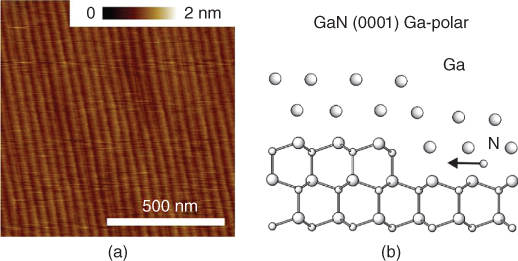
Figure 12.1 (a) Surface morphology of c‐plane GaN grown by PAMBE. Step‐flow growth mode is observed. (b) Schematics of vicinal GaN surface during epitaxy under metal excess. The nitrogen atom traveling below the Ga bilayer has a low diffusion barrier.
The explanation of the high‐quality growth at low temperature was given by Neugebauer et al. [29]. The existence of a very efficient lateral diffusion channel for nitrogen adatoms on (0001) GaN surface just below the thin metallic adlayer was postulated. This is presented schematically in Figure 12.1(b). It was calculated that the energetic barrier for the diffusion of nitrogen adatoms is substantially lower in the presence of the Ga or In metal adlayer, formed during metal‐rich conditions, than for the bare surface [29]. Therefore, low diffusion barriers for this so‐called adlayer‐enhanced lateral diffusion (AELD) facilitate high‐quality step‐flow epitaxy at low temperatures [ 9 14– 16, 18, 27 30–32]. These growth conditions, where liquid metal is present at the surface, are similar to the liquid phase epitaxy process.
The need for high nitrogen overpressure becomes a limiting factor for InGaN growth. There are two strategies for the growth of high‐In‐content InGaN layers. The first relies on lowering the growth temperature [33,34], while the second is based on increased N flux [ 21,35]. It is straightforward and easy in practical realization to increase the In content by lowering the growth temperature, but as a result, the quality of grown InGaN layers is worse for increased In composition [21]. The most likely reason for such degradation is low nitrogen adatom diffusion at lower growth temperature. As a result, nucleation of In‐rich regions can occur with all the negative consequences on optical layer quality and morphology. On the other hand, the advantages of the second approach, which relies on high N flux are: (i) reduced In content fluctuations in the InGaN layers, which decreases the density of localized states [21] and (ii) improved quality of the interfaces between quantum wells (QWs) and quantum barriers (QBs) [36]. The role of the different growth parameters – like N, Ga fluxes, growth temperature, or substrate miscut – for the In‐rich regime in PAMBE were studied experimentally and theoretically in detail in Refs. [ 35,37]. In Figure 12.2(a) we show the experimental dependence of the In content as a function of Ga flux for constant nitrogen flux equal to 0.35 µm h−1 and growth temperature of 650 °C for In‐rich growth conditions. The solid line is a result of phenomenological model calculations, which assumes the existence of two nonequivalent atomic steps related to the wurtzite structure [35]. Within this model we can successfully predict the In content for different growth temperatures, nitrogen and gallium fluxes. As one can see in Figure 12.2(a), when we reduce the Ga flux from equal to the N flux, an almost linear increase of the In content is observed. Saturation of the In content is related to the thermal stability of InGaN. InGaN decomposition can be prevented by increasing the nitrogen flux. Figure 12.2(b) presents the theoretically predicted dependence of In content as a function of Ga flux for different values of N flux at constant growth temperature. It is worth noting that the same InGaN composition has to be grown at different Ga/N ratios when the N flux is varied. The maximum In content in InGaN [depicted as stars in Figure 12.2(b)] is limited by the decomposition rate of InGaN during growth. One can see that this value gets higher when the active N flux increases. However, the increase in maximum In content depends logarithmically on N flux. Therefore, for substantial increase of In content in InGaN layers, we have to apply huge amounts of active nitrogen.

Figure 12.2 (a) Indium content for InGaN layers grown using various gallium fluxes. The blue solid line represents the predicted InGaN compositions according to the model from Ref. [35]. (b) The In content x as a function of Ga flux for five different N fluxes at constant growth temperature 650 °C. Stars indicate maximum In content for each nitrogen flux.
The amount of active nitrogen flux used for InGaN growth impacts its optical quality. In Figure 12.3(a, b) we compare the time‐resolved photoluminescence (TRPL) spectra for two multi‐quantum wells (MQWs) samples grown with low and high nitrogen flux, respectively. Both MQWs structures have maximum photoluminescence (PL) around λ = 520 nm, but the spectral dependence of PL decay time τPL(λ) for sample (a) is qualitatively different than for sample (b). For sample (a) grown with low nitrogen flux, τPL increases from 3 ns at λ=485 nm to 13 ns at λ=570 nm. Such a spectral dispersion of τPL implies carrier localization and can be attributed to In content fluctuations [21]. Localization can effectively reduce the performance of LDs and is strongly undesirable [38].
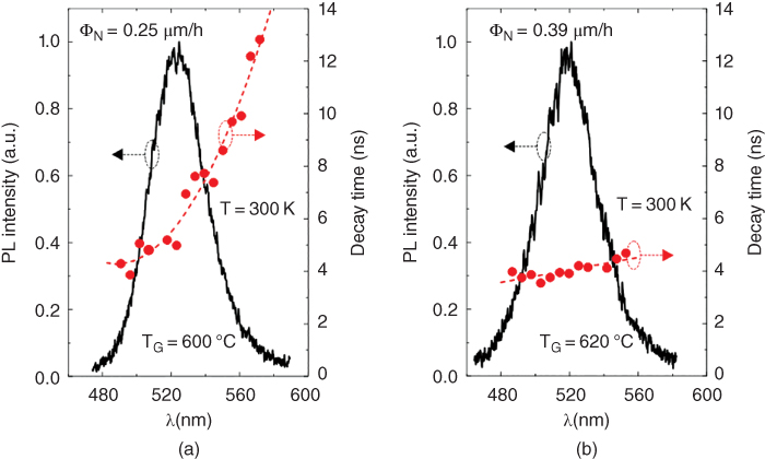
Figure 12.3 PL intensity and its decay time for MQW structures grown by PAMBE using (a) low and (b) high nitrogen flux.
The other benefit of the use of high N flux for InGaN layer growth is the reduction in surface roughness, which can drastically improve the QW–barrier interface abruptness. In Figure 12.4(a, b) we present AFM images of two 30 nm In0.17Ga0.83N layers, both grown at the same temperature (650 °C) but using two different N fluxes of 0.3 and 0.9 µm h−1, respectively [36]. The Ga fluxes were adjusted appropriately to obtain the same In composition. The root mean square (RMS) roughness measured on a 1 × 1 µm2 AFM scan decreased from 0.52 nm for the layer grown at lower N flux to 0.39 nm for the layer grown using higher N flux. Qualitatively, for the higher N flux a smoother surface with visible atomic step edges was grown, while for the low N flux the surface was substantially rougher with numerous deep trenches and no clear atomic steps. For the low N flux sample the local surface orientation changes from place to place, which means that we can expect In incorporation inhomogeneity, since the In content in InGaN layers depends on substrate miscut [37].
Figure 12.4 Surface morphology of 30 nm In0.17Ga0.83N layers grown using nitrogen fluxes equal to (a) 0.3 µm h−1 and (b) 0.9 µm h−1.
As a consequence, the PL line width for InGaN QWs grown by PAMBE can be efficiently reduced by application of high nitrogen flux. In Figure 12.5(a) we demonstrate the room‐temperature PL of 3 nm In0.17Ga0.83N/7 nm In0.08Ga0.92N MQWs emitting at λ = 450 nm grown using two different N fluxes. The QWs were grown using the same growth conditions as for the InGaN layers shown in Figure 12.4. As can be seen in Figure 12.5(a), by increasing the N flux from 0.3 to 0.9 µm h−1, we reduced the PL full‐width at half‐maximum (FWHM) from 22 down to 14 nm. A smaller PL FWHM leads to better performance of LDs due to narrowing of the gain spectra. To confirm the relation between narrowing of the PL line for QWs and increase in N flux used for growth, in Figure 12.5(b) we present PL FWHM as a function of emission wavelength for QW structures grown with different N fluxes. It is important to point out that we observed a systematic narrowing of the PL lines for all QWs structures grown with higher N flux. The demonstrated pronounced narrowing of the PL lines for longer wavelengths is an important milestone on the path towards PAMBE‐grown green LDs.

Figure 12.5 (a) PL spectra of two MQWs structures grown by PAMBE using active nitrogen flux of 0.3 and 0.9 µm h−1. (b) PL FWHM as a function of the emission wavelength for InGaN MQWs grown with active nitrogen fluxes of 0.3, 0.9, 2, and 3 µm h−1.
12.3 Applications of PAMBE in Growth of Nitride Laser Diodes
The first nitride LDs were demonstrated by S. Nakamura in 1996 using MOVPE [3]. The attempt to repeat this using MBE was unsuccessful for many years, until in 2004 the first 405 nm violet InAlGaN LDs were grown by ammonia MBE at Sharp Laboratories Europe Ltd. [ 7, 8]. These LDs were grown under nitrogen‐rich conditions, making use of the similar growth mechanism as in MOVPE. The high growth temperature, high ammonia flux conditions, and corrosive nature of ammonia were very demanding for the MBE technology. On the other hand, development of the low‐temperature GaN and InGaN growth by PAMBE (described in Section 12.2) led to a substantial improvement in crystal quality obtained by this ammonia‐free technique. Shortly after the demonstration of LDs by ammonia‐MBE, we demonstrated nitride blue‐violet LDs by PAMBE [9].
Presently, the nitride LD market is dominated by devices grown by MOVPE. However, recent advances in material quality of InGaN might create a niche for PAMBE‐grown LDs. The possibility of thick, low In content layers grown without the generation of extended defects facilitates their incorporation as waveguides in LD structures. Such device architecture has some important advantages over the conventional one, which comprises AlGaN claddings and GaN waveguides. Namely, four features of LDs with InGaN waveguide are of particular interest. First is the enhancement of the optical confinement factor (Γ), which will be discussed in Section 12.3.1 [39]. Second, shown in Section 12.3.2, is a full elimination of the leakage of optical modes to the GaN substrate [40]. Third is the simplified epitaxial structure of LD, in which the AlGaN claddings can be much thinner [40]. Fourth, related to the strain compensation of the whole laser structure, it is possible to get a flat wafer with LD epitaxial structure by choosing an appropriate thickness of AlGaN claddings and InGaN waveguides. The suppression of wafer bowing can become extremely important for the processing of LDs grown on large‐diameter substrates. Furthermore, the increase in efficiency of InGaN QWs grown with high active nitrogen flux enabled the demonstration of long‐wavelength nitride LDs, which will be described in Section 12.3.3. The two most important parameters enabling the application of LDs are: maximum optical power and lifetime of the devices. These will be described in Sections 12.3.4 and 12.3.5, respectively.
The LDs presented in this work were grown on high‐quality, low dislocation density freestanding ammono‐GaN substrates [41]. The threading dislocation density of the substrate was below 105 cm−2 and the miscut 0.5–0.8°. Details on the growth and processing of the devices can be found in Refs. [ 19, 36,42].
Three different concepts of LD structure are presented in Figure 12.6 to show the potential applications of thick InGaN waveguides. Figure 12.6(a) shows a reference structure with InGaN used only in the MQW region. Figure 12.6(b) presents the LD structure with InGaN waveguides used complementarily with AlGaN claddings to increase light confinement in the structure and decrease wafer bowing. In Figure 12.6(c) an Al‐free LD structure is shown, where the InGaN waveguides are the only source of refractive index contrast. The important difference lies in the fact that LDs with an InGaN waveguide can have much thinner bottom claddings without causing light leakage to the GaN substrate.
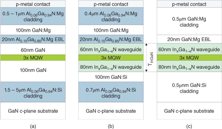
Figure 12.6 Schematics of LD structures: (a) conventional with thick AlGaN claddings; (b) with InGaN waveguides and thin AlGaN claddings; and (c) AlGaN cladding‐free.
Figure 12.7(a) presents an X‐ray diffraction reciprocal space map of the whole LD structure, showing that the 160 nm thick In0.08Ga0.92N waveguide is fully strained to the GaN substrate and AlGaN claddings. Figure 12.7(b) presents a large area scanning transmission electron microscope (STEM) image of a PAMBE‐grown LD. No lattice relaxation or extended defect formation is observed, even though the critical thickness for InGaN relaxation reported in the literature exceeded [43]. Figure 12.7(c) shows a high‐resolution STEM image of the active region.
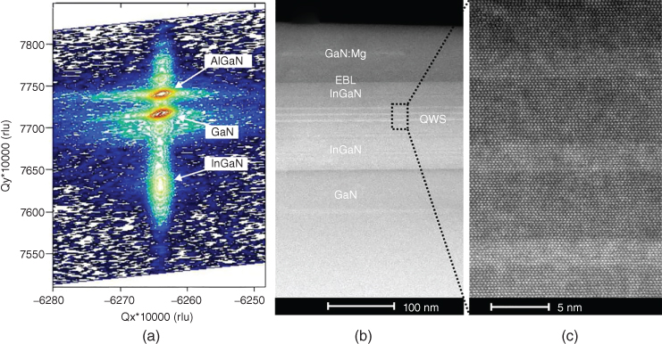
Figure 12.7 (a) Reciprocal space map of a symmetric  reflection of a full LD structure with thick InGaN waveguides showing no relaxation. (b) STEM image of a PAMBE‐grown LD structure taken along the
  zone axis. (b) HRSTEM image of the active region.
12.3.1 Enhancement of Optical Confinement Factor by InGaN Waveguide
The influence of the InGaN waveguide on properties of LDs was studied theoretically by Zhang et al. and Huang et al. [44,45], who found that Γ increases with increasing In content. To fully benefit from the enhancement of Γ, the optical losses due to absorption of the layer have to be minimized. InGaN layers are known to suffer from In fluctuations, which additionally increase the optical losses. Son et al. have shown that the absorption loss of an In0.01Ga0.99N waveguide can be as high as αInGaN = 40 cm−1 for λ = 405 nm [46]. Thus, maintaining high quality in InGaN waveguides is crucial.
The influence of the InGaN waveguide on Γ was studied in blue (λ = 450 nm) LDs. A calculation of the optical mode distribution is presented in Figure 12.8 for two compositions of InxGa1−xN waveguide, x = 0.04 and 0.08. As can be seen, the optical mode is much better confined within the active region in case of higher InGaN waveguide composition. The calculated Γ increased from 0.028 to 0.035. Additionally, the part of the optical field propagating in the p‐doped region is reduced. This will decrease the optical losses due to absorption on the Mg‐doped layers [47,48].
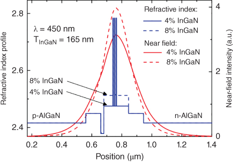
Figure 12.8 Refractive index profile and optical mode distribution for LDs with x = 0.04 and 0.08 InxGa1−xN composition.
To study the influence of InGaN waveguide composition on Γ, the optical gain (G) has been measured with the Hakki–Paoli technique [49]. The optical gain spectra are collected below the lasing threshold and their maxima are extracted and shown in Figure 12.9(a) as a function of current density. The differential gain dG/dj is given by a linear approximation of the data shown in Figure 12.9(a), and its value at j = 0 is close to the value of internal optical losses αint. A detailed description of the experimental scheme can be found in Refs. [ 39,50].
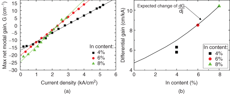
Figure 12.9 (a) Dependence of the maximum net modal gain on current density. The solid lines represent the fit of the differential gain. (b) Dependence of differential gain on InGaN waveguide composition. The solid line represents the calculated change due to the change in Γ and carrier wavefunction overlap.
Firstly, the influence of InGaN waveguide composition on the differential gain will be discussed. The optical gain is given by G = ηiΓg, where ηi is the carrier injection efficiency and g is the material gain of the QWs. The slope efficiency was measured and showed no difference in ηi between the LDs [39]. Furthermore, the three LDs were grown with the same QWs, so only a small variation of g between them is expected. The LDs with active region having higher In content QBs will have a higher overlap of the electron and hole wavefunctions due to decreased built‐in electric fields inside the QWs [51]. The extracted values of differential gain are presented in Figure 12.9(b), together with the calculated expected change of dG/dj. The expected change is primarily due to enhancement of Γ with increased In content. The differential gain is 6.1, 8.5, and 10.4 cm kA−1 for InGaN waveguide compositions of x = 0.04, 0.06, and 0.08, respectively. The change between the LDs with x = 0.06 and 0.08 is well reproduced by the calculations, but the LDs with x = 0.04 have a slightly lower differential gain. This is due to light leakage to the GaN substrate and will be discussed in Section 12.3.2 .
Secondly, the influence of InGaN composition on the optical losses of the LD will be presented. The optical losses extracted from the optical gain measurements are αint = 17, 20, and 24 cm−1 for LDs with x = 0.04, 0.06, and 0.08, respectively. The increase in internal losses can be approximated to increase by 2 cm−1 for every percentage of In added to the waveguide. It is possible that the internal losses due to absorption on higher In content InGaN waveguides can be decreased by further improvement in crystal quality.
12.3.2 Elimination of Light Leakage to GaN Substrate Using a Thick InGaN Waveguide
The nitride LDs suffer from leakage of light to the substrate [52–57]. This happens if the thickness of the n‐AlGaN cladding is insufficient [58,59]. Unfortunately, the large lattice mismatch between AlGaN alloys and GaN substrate substantially limits the thickness of the cladding [60]. In case of blue and green nitride LDs, the leakage is even more pronounced and growth of AlGaN claddings with sufficient thickness becomes challenging [56, 57]. This leakage is visible as a ripple in the far‐field pattern of the LD, and causes major limitations in applications as it degrades the optical beam quality [57].
A unique feature of InGaN waveguides is that they allow us to fully suppress the leakage to the substrate without the need for thick AlGaN claddings [40]. Figure 12.10(a) presents the calculated dependence of light leakage loss (αloss) to GaN substrate on InGaN waveguide composition. The thickness of the InGaN waveguide is 145 nm and the thickness of the AlGaN cladding is set to be 700 nm, which is too small to prevent leakage, even in case of violet LDs [58]. Further details of the calculations can be found in Ref. [40]. With increased In content in the range of x = 0–0.04, the leakage loss constantly decreases. Strikingly, the drop of αloss becomes more rapid as the In content is further increased and at a certain “cut‐off” InGaN composition the leakage is fully suppressed. It is worth noting that this “cut‐off” InGaN composition does not depend on the thickness of the AlGaN cladding but only on its composition.

Figure 12.10 (a) Dependence of light leakage to GaN substrate on InGaN composition. (b) Dependence of effective refractive index of the propagating mode on InGaN composition. The dashed red line represents the refractive index of the substrate above which no leakage to the GaN substrate is present.
(Source: After Muziol et al. [40].)
The reason behind this elimination of light leakage is the change in effective refractive index neff of the propagating mode. Figure 12.10(b) presents the calculated dependence of neff on InGaN composition. neff increases together with the In content and at the “cut‐off” InGaN composition surpasses the refractive index of the GaN substrate shown as a red dashed line. Above this level there is no leakage of optical modes to the GaN substrate, no matter what the n‐AlGaN cladding thickness.
Figure 12.11(a) presents a schematic drawing of the LD device together with the emitted beam. The far‐field pattern measured by a charge‐coupled device camera (CCD) for LDs with x = 0.04 and 0.08 are presented in Figure 12.11(b, c), respectively. In case of the LD with InGaN waveguide x = 0.04, the optical beam is deteriorated by an additional peak at 10° on the side of the substrate. This is a clear indication of light leakage to the substrate. On the other hand, the far field of the LD with x = 0.08 is Gaussian‐shaped with no additional peaks. In this case there is no leakage of light to the GaN substrate. The LD with InGaN waveguide x = 0.06 also did not show any additional peaks in the far‐field pattern [40].
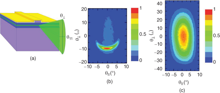
Figure 12.11 (a) Schematics of a ridge waveguide laser diode with the emitted optical beam. Far‐field patterns of LDs with InxGa1−xN waveguide composition of (b) x = 0.04 and (c) x = 0.08.
12.3.3 Long‐Wavelength Laser Diodes by PAMBE
To accommodate new possible applications for LDs grown by PAMBE, devices operating at longer wavelength were studied. To increase the emission wavelength, the In content in InGaN QWs needs to be increased. The most commonly used way of increasing In incorporation into the InGaN layer (in both MOVPE and PAMBE) is to lower the growth temperature, although it has been shown that a more efficient approach for PAMBE growth is to increase the N flux used during QWs growth. As mentioned in Section 12.2 , the maximum In content as a function of N flux at constant temperature follows a logarithmic dependence. The expected maximum In content for growth temperature of 650 °C is presented in Figure 12.12(a).
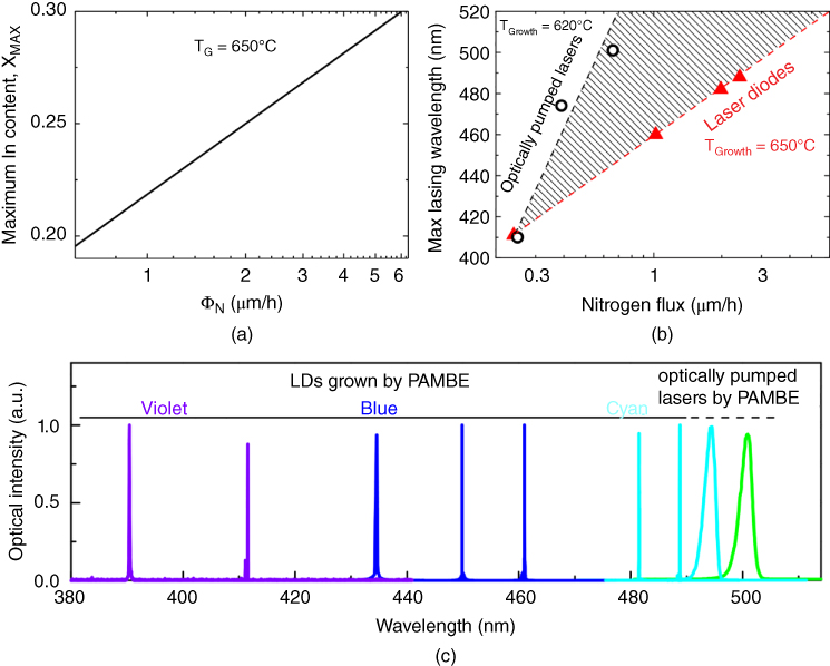
Figure 12.12 (a) The maximum In content at 650 °C as a function of the nitrogen flux predicted with the model from Ref. [35]. (b) Maximum lasing wavelength as a function of nitrogen flux used for the growth of QWs. Data points are plotted for optically pumped structures grown at 620 °C (black circles) and electrically pumped laser diodes (red triangles). (c) Lasing spectra of LDs and optically pumped structures grown by PAMBE.
Firstly, optically pumped structures were studied. Single InGaN QW structures were grown sandwiched between AlGaN claddings. For that series of samples, active regions were grown at 620 °C using N flux reaching 0.6 µm h−1. No p‐ and n‐type dopants were used for growth. As reported in Ref. [21], lasing up to λ = 501 nm was obtained. Experimental data for this series of samples are presented in Figure 12.12(b) (black circles). The quality of the active region obtained in this way was sufficient for optically pumped structures where high pumping power density can easily be used.
In parallel with optically pumped structures, long‐wavelength electrically driven LDs were developed [ 19, 20, 42]. To increase the efficiency of the obtained structures, a higher growth temperature had to be used for the active region in this case. All InGaN/InGaN QWs were grown at 650 °C using N flux reaching up to 2.4 µm h−1. It is important to point out that obtaining such a high growth rate for the PAMBE system is technically challenging. The main problem is the plasma source efficiency, defined as the amount of activated nitrogen to total injected nitrogen, which is limited to roughly 1%. To increase the accessible growth rate, the pumping capabilities of the PAMBE reactor had to be increased drastically by installing three cryogenic pumps on the growth chamber. This improvement enabled the demonstration of long‐wavelength PAMBE‐grown LDs. Figure 12.12(b) presents the maximal achieved lasing wavelength as a function of the nitrogen flux for optically and electrically pumped lasers. All experimental data for LDs presented in Figure 12.12(b) were obtained for devices operating in CW mode at room temperature. The maximum lasing wavelength increased logarithmically with nitrogen flux used for the growth of the active region, which stays in good agreement with the predictions of our model presented in Figure 12.12(a) and the statement that increasing In content by increasing nitrogen flux keeps high crystal quality. Figure 12.12(c) illustrates the emission spectra of PAMBE‐grown LDs from violet (λ = 388 nm [22]) through blue [ 9, 19, 42] to cyan (λ = 489 nm [20]) with optically pumped laser structures emitting in green 501 nm [21].
12.3.4 High‐Power Blue Laser Diodes by PAMBE
To study the maximum optical power in CW mode, the LD was mounted in copper clamps to ensure good heat dissipation. The facets of the LD were left uncoated, so the light was emitted equally to both sides. Figure 12.13 presents the light–current–voltage (L–I–V) characteristics collected at room temperature. The threshold current and threshold voltage were Ith = 250 mA and Vth = 5 V, respectively. The maximum optical power was 0.5 W per facet. The optical power was limited by the catastrophic optical damage (COD), which was observed for several devices at the same optical power level. The very high characteristic temperature of T0 = 160 K allowed us to operate the device in CW mode up to 60 °C with no visible change in slope efficiency.
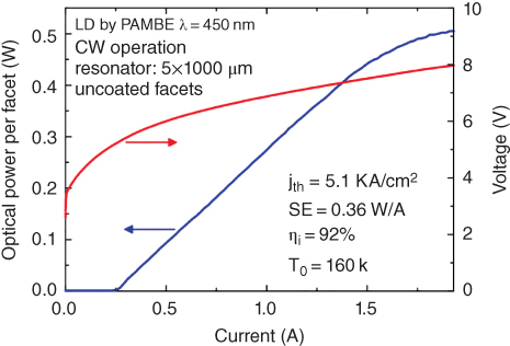
Figure 12.13 L–I–V characteristics of a high‐power LD grown by PAMBE.
(Source: After Muziol et al. [61].)
12.3.5 Lifetime of PAMBE Laser Diodes
Device lifetime is one of the most crucial LD parameters when applications are considered. The lifetime will be defined here as the time after which the threshold current increases, due to device degradation, by 50% compared to its initial value. The differences in growth conditions between MOVPE and PAMBE results in a different LD degradation mechanism [62]. This enforces separate optimization methods and can expose some limitations of the MOVPE method.
Figure 12.14(a) presents the dependence of the threshold current density on time during constant electrical stress for three LDs fabricated in 2012, 2014, and 2016. The tests were conducted at room temperature with the operating current adjusted to obtain a constant optical power of 15 mW. The lifetime is approximated assuming a linear degradation. The lifetime of the first PAMBE‐grown LDs was on the order of a few hours (year 2005) [16]. Advancements in material quality, processing, and packaging of the LDs led to substantial increases in lifetime, up to 2000 hours (year 2012) [19]. However, these devices still suffered from a large number of dislocations generated during electron blocking layer (EBL) growth, as presented in Figure 12.14(b). Further advancement in the understanding of growth of low‐temperature AlGaN used in the EBL led to removal of this problem [63]. Figure 12.14(c, d) presents scanning electron microscopy (SEM) images of the LD structures after defect selective etching, revealing the dislocation density. Before optimization, for the LD living 2000 hours, the etch pit density (EPD) was on the order of 108 cm−2. For the LD with improved material quality of the EBL this value decreased to 106 cm−2 and a lifetime of 15 000 hours was obtained (year 2014). Presently, after further development of the material quality, the estimated lifetime of the devices is 100 000 hours (year 2016). This extremely large value lets us compare our results to the Al‐free infrared LDs where almost no degradation is visible [64,65].
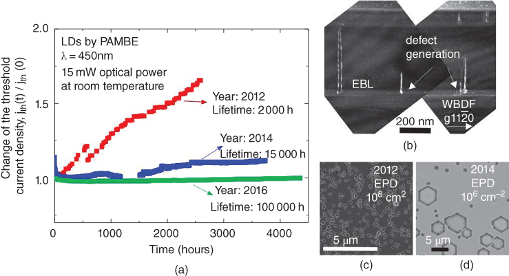
Figure 12.14 (a) Time dependence of the change in threshold current density during reliability studies of laser diodes grown by PAMBE. (b) Cross‐sectional TEM images of the PAMBE laser diode under weak‐beam dark‐field (WBDF) conditions  showing defect generation in EBL. (c), (d) SEM images of LD structures after defect‐selective etching with EPD of 108 and 106 cm−2, respectively.
12.4 New Concepts of LDs with Tunnel Junctions
One of the most challenging issues for nitride‐based devices like LEDs and LDs is poor conductivity of the p‐type region [5]. The resistance of the p‐type contact determines the performance and constrains the design of InGaN LEDs and LDs. Recently, there has been increasing attention given to interband TJs for effective carrier conversion between n‐type and p‐type material in nitride LEDs and LDs [66–72]. Efficient TJs may find very important application to inject holes into the p‐type region of LDs and LEDs, opening up possibilities for new architecture of these devices. For LDs it can create the possibility of growing stacks of LDs operating in the range of hundreds of watts in pulse mode (violet‐green region), as demonstrated for infrared GaAs LDs. The application of TJs will also be extremely important for (i) UV LDs and LEDs, where the challenges for p‐type conductivity are more serious (due to the larger Mg activation energy) than for visible optoelectronics and (ii) designing new architectures of monolithic vertical cavity surface emitting lasers (VCSELs). In spite of extensive efforts, there are no nitride devices with TJs available on the market due to fundamental challenges with the activation of p‐type conductivity in buried Mg‐doped layers in devices grown by the commonly used MOVPE. The intrinsic barrier for MOVPE is due to the fact that hydrogen cannot diffuse through n‐type layers. If a Mg‐doped nitride layer is overgrown by an n‐type layer, the activation of p‐type conductivity, which relays on the partial hydrogen removal, is blocked. The attempt to overcome this problem by hydrogen removal through etched trenches did not give satisfactory results [73]. The p‐type layers grown by PAMBE do not need post‐growth activation, which makes this technique a powerful tool for the realization of TJs. The successful application of TJs to optoelectronic devices was made by hybrid growth – where the optical part of the device was made by MOVPE while the TJ was made by MBE [ 66–68].
In this section we present TJ LDs operating at λ = 450 nm entirely made by PAMBE. We changed the conventional design of PAMBE LDs, adding a TJ on top, as presented in Figure 12.15(a). For wide‐bandgap semiconductors, the most important issue in order to achieve high transmission currents through the junction is engineering of the depletion layer. We make use of the concept, where the built‐in field generated by the growth of the InGaN QWs strongly decreases the depletion width of the TJ region and enhances carrier transmission probability [ 66,71]. Figure 12.15(b) presents the L–I–V characteristics of LDs with a conventional metal contact to p‐type and a TJ. The resonator lengths are 1 mm with uncoated facets. The threshold current density and slope efficiency of the TJ LD are equal to jth = 3.2 kA cm−2 and η = 0.6 W A−1, respectively, and are similar to the values of the LD with conventional contacts. The operating voltage is increased by 0.6–0.8 V, which can be attributed to the additional voltage loss in the TJ region. The fact that the addition of the TJ does not deteriorate the LD parameters opens new perspectives on growing stacks of LDs.
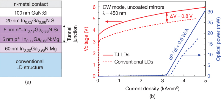
Figure 12.15 (a) Schematic diagram of LD with a tunnel junction contact instead of a conventional metal contact to p‐type layers. (b) L–I–V characteristics of conventional LD (dashed lines) and TJ LD (solid lines). Both LDs are operating at CW mode at λ = 450 nm.
12.5 Summary
In this chapter we presented the recent development in PAMBE of nitride‐based LDs. The following milestones contribute to the progress in material quality of layers grown by PAMBE: (i) application of the low‐temperature growth mechanism with a thin metal layer at the surface during growth in the so‐called “liquid phase epitaxy‐like” regime; (ii) development of an In incorporation model; (iii) understanding of the essential role of high active nitrogen flux during the growth of InGaN; and (iv) use of low dislocation density bulk GaN substrates.
It was demonstrated that PAMBE allows us to grow thick, high‐quality InGaN on (0001) GaN, which opens up a new perspective for nitride LDs with InGaN waveguides. The influence of the InGaN waveguides on optical gain and light leakage to the GaN substrate was studied. LDs containing InGaN waveguides with excellent optical beam quality have been demonstrated.
The PAMBE LDs operate in a range of λ = 388–489 nm. The low dislocation density GaN substrates allowed us to fabricate CW LDs with lifetime exceeding 100 000 hours. We observe an increase in maximum lasing wavelength with increased active nitrogen flux applied during QWs growth. Lasing at 489 nm was obtained for 2.4 µm h−1 of active nitrogen flux. As can be seen from the above results, PAMBE can be a viable technology for growth of nitride LDs. Thus, the long‐term prospects for PAMBE in this area appear to be as good as for MOVPE.
Acknowledgments
This work was partially supported by the Polish National Center for Research and Development Grant PBS3/A3/23/2015, Foundation for Polish Science TEAM TECH/2016‐2/12, and Polish National Center for Research and Development Grant LIDER/29/0185/L‐7/15/NCBR/2016. We would like to thank P. Perlin, T. Suski, P. Wisniewski, I. Grzegory, Z. R. Wasilewski, S. Porowski, M. Boćkowski, J. Smalc‐Koziorowska, J. Borysiuk, S. Grzanka, E. Grzanka, G. Nowak, J. Weyher, L. Marona, R. Kudrawiec, M. Krysko, S. Krukowski, A. Sarzyńska, A. Nowakowska‐Szkudlarek, and W. Purgal for support with experiments, discussions, laser processing, and testing.
References
- 1 Morkoç, H. (2009). General properties of nitrides. In: Handbook of Nitride Semiconductors and Devices, 1–129. Weinheim: Wiley‐VCH.
- 2 Ehrentraut, D., Meissner, E., and Bockowski, M. (2010). Technology of Gallium Nitride Crystal Growth. Berlin: Springer.
- 3 Nakamura, S., Fasol, G., and Pearton, S. (2000). The Blue Laser Diode: The Complete Story. Berlin: Springer.
- 4 Nakamura, S., Senoh, M., Nagahama, S.‐i. et al. (1996). Japanese Journal of Applied Physics 35: L74.
- 5 Nakamura, S., Senoh, M., Nagahama, S.‐i. et al. (1997). Applied Physics Letters 70: 868.
- 6 DenBaars, S.P., Feezell, D., Kelchner, K. et al. (2013). Acta Materialia 61: 945.
- 7 Kauer, M., Hooper, S.E., Bousquet, V. et al. (2005). Electronics Letters 41: 739.
- 8 Hooper, S.E., Kauer, M., Bousquet, V. et al. (2004). Electronics Letters 40: 33.
- 9 Skierbiszewski, C., Wasilewski, Z.R., Siekacz, M. et al. (2005). Applied Physics Letters 86: 011114.
- 10 Morkoç, H. (2001). Journal of Materials Science: Materials in Electronics 12: 677.
- 11 Riechert, H., Averbeck, R., Graber, A. et al. (1997). Materials Research Society Symposium Proceedings 449: 149.
- 12 Chen, H. (2000). Journal of Vacuum Science and Technology B 18: 2284.
- 13 Zywietz, T., Neugebauer, J., and Scheffler, M. (1998). Applied Physics Letters 73: 487.
- 14 Heying, B., Averbeck, R., Chen, L.F. et al. (2000). Journal of Applied Physics 88: 1855.
- 15 Waltereit, P., Sato, H., Poblenz, C. et al. (2004). Applied Physics Letters 84: 2748.
- 16 Skierbiszewski, C., Wiśniewski, P., Siekacz, M. et al. (2006). Applied Physics Letters 88: 221108.
- 17 Skierbiszewski, C., Dybko, K., Knap, W. et al. (2005). Applied Physics Letters 86: 102106.
- 18 Manfra, M.J., Baldwin, K.W., Sergent, A.M. et al. (2004). Applied Physics Letters 85: 5394.
- 19 Skierbiszewski, C., Siekacz, M., Turski, H. et al. (2012). Applied Physics Express 5.
- 20 Turski, H., Muziol, G., Wolny, P. et al. (2014). Applied Physics Letters 104: 023503.
- 21 Siekacz, M., Sawicka, M., Turski, H. et al. (2011). Journal of Applied Physics 110: 063110.
- 22 Sawicka, M., Muziol, G., Turski, H. et al. (2013). Applied Physics Letters 102: 251101.
- 23 Sawicka, M., Muziol, G., Turski, H. et al. (2014). Journal of Vacuum Science & Technology B 32: 02C115.
- 24 Karpiński, J. and Porowski, S. (1984). Journal of Crystal Growth 66: 11.
- 25 Ambacher, O. (1998). Journal of Physics D: Applied Physics 31: 2653.
- 26 Elsass, C.R., Smorchkova, I.P., Heying, B. et al. (1999). Applied Physics Letters 74: 3528.
- 27 Heying, B., Tarsa, E.J., Elsass, C.R. et al. (1999). Journal of Applied Physics 85: 6470.
- 28 Adelmann, C., Brault, J., Jalabert, D. et al. (2002). Journal of Applied Physics 91: 9638.
- 29 Neugebauer, J., Zywietz, T.K., Scheffler, M. et al. (2003). Physical Review Letters 90: 056101.
- 30 Skierbiszewski, C., Wasilewski, Z., Siekacz, M. et al. (2004). Physica Status Solidi A 201: 320.
- 31 Northrup, J.E., Neugebauer, J., Feenstra, R.M., and Smith, A.R. (2000). Physical Review B 61: 9932.
- 32 Skierbiszewski, C., Siekacz, M., Perlin, P. et al. (2007). Journal of Crystal Growth 305: 346.
- 33 Averbeck, R. and Riechert, H. (1999). Physica Status Solidi A 176: 301.
- 34 Skierbiszewski, C., Wasilewski, Z.R., Grzegory, I., and Porowski, S. (2009). Journal of Crystal Growth 311: 1632.
- 35 Turski, H., Siekacz, M., Wasilewski, Z.R. et al. (2013). Journal of Crystal Growth 367: 115.
- 36 Skierbiszewski, C., Siekacz, M., Turski, H. et al. (2013). Journal of Crystal Growth 378: 278.
- 37 Turski, H., Siekacz, M., Sawicka, M. et al. (2011). Journal of Vacuum Science & Technology B 29: 03C136.
- 38 Kojima, K., Funato, M., Kawakami, Y. et al. (2006). Applied Physics Letters 89: 241127.
- 39 Muziol, G., Turski, H., Siekacz, M. et al. (2015). Applied Physics Express 8: 032103.
- 40 Muziol, G., Turski, H., Siekacz, M. et al. (2016). Applied Physics Express 9: 092103.
- 41 Dwiliński, R., Doradziński, R., Garczyński, J. et al. (2009). Journal of Crystal Growth 311: 3015.
- 42 Skierbiszewski, C., Turski, H., Muziol, G. et al. (2014). Journal of Physics D: Applied Physics 47: 073001.
- 43 Leyer, M., Stellmach, J., Meissner, C. et al. (2008). Journal of Crystal Growth 310: 4913.
- 44 Huang, C.‐Y., Lin, Y.‐D., Tyagi, A. et al. (2010). Journal of Applied Physics 107: 023101.
- 45 Zhang, L.Q., Jiang, D.S., Zhu, J.J. et al. (2009). Journal of Applied Physics 105: 023104.
- 46 Son, J.K., Lee, S.N., Paek, H.S. et al. (2008). Journal of Applied Physics 103: 103101.
- 47 Kuramoto, M., Sasaoka, C., Futagawa, N. et al. (2002). Physica Status Solidi A 192: 329.
- 48 Uchida, S., Takeya, M., Ikeda, S. et al. (2003). IEEE Journal of Selected Topics in Quantum Electronics 9: 1252.
- 49 Hakki, B.W. and Paoli, T.L. (1973). Journal of Applied Physics 44: 4113.
- 50 Muziol, G., Turski, H., Siekacz, M. et al. (2013). Applied Physics Letters 103.
- 51 Takeuchi, T., Wetzel, C., Yamaguchi, S. et al. (1998). Applied Physics Letters 73: 1691.
- 52 Nakamura, S. (1997). Materials Science and Engineering: B 50: 277.
- 53 Takeuchi, T., Detchprohm, T., Iwaya, M. et al. (1999). Applied Physics Letters 75: 2960.
- 54 Nakamura, S., Senoh, M., Nagahama, S.‐i. et al. (1998). Japanese Journal of Applied Physics 37: L1020.
- 55 Laino, V., Roemer, F., Witzigmann, B. et al. (2007). IEEE Journal of Quantum Electronics 43: 16.
- 56 Lermer, T., Schillgalies, M., Breidenassel, A. et al. (2010). Physica Status Solidi A 207: 1328.
- 57 Strauss, U., Eichler, C., Rumbolz, C. et al. (2008). Physica Status Solidi C 5: 2077.
- 58 Hatakoshi, G.‐I. (2003). Optical Review 10: 307.
- 59 Bergmann, M.J., Casey, H.C. Jr., Nakamura, S. et al. (1998). Journal of Applied Physics 84: 1196.
- 60 Einfeldt, S., Kirchner, V., Heinke, H. et al. (2000). Journal of Applied Physics 88: 7029.
- 61 Muziol, G., Siekacz, M., Turski, H. et al. (2015). Journal of Crystal Growth 425: 398.
- 62 Bojarska, A., Muziol, G., Skierbiszewski, C. et al. (2017). Applied Physics Express 10: 091001.
- 63 Skierbiszewski, C., Siekacz, M., Turski, H. et al. (2012). Journal of Vacuum Science & Technology B 30.
- 64 Eliashevich, I., Diaz, J., Yi, H. et al. (1995). Applied Physics Letters 66: 3087.
- 65 Diaz, J., Yi, H.J., Razeghi, M., and Burnham, G.T. (1997). Applied Physics Letters 71: 3042.
- 66 Krishnamoorthy, S., Akyol, F., and Rajan, S. (2014). Applied Physics Letters 105: 141104.
- 67 Young, E.C., Yonkee, B.P., Wu, F. et al. (2016). Applied Physics Express 9: 022102.
- 68 Leonard, J.T., Young, E.C., Yonkee, B.P. et al. (2015). Applied Physics Letters 107: 091105.
- 69 Malinverni, M., Martin, D., and Grandjean, N. (2015). Applied Physics Letters 107: 051107.
- 70 Malinverni, M., Tardy, C., Rossetti, M. et al. (2016). Applied Physics Express 9: 061004.
- 71 Krishnamoorthy, S., Akyol, F., Park, P.S., and Rajan, S. (2013). Applied Physics Letters 102: 113503.
- 72 Simon, J., Zhang, Z., Goodman, K. et al. (2009). Physical Review Letters 103: 026801.
- 73 Kuwano, Y., Kaga, M., Morita, T. et al. (2013). Japanese Journal of Applied Physics 52: 08JK12.