
2
General Description of MBE
Yoshiji Horikoshi
Department of Science and Engineering, Waseda University, Tokyo, 169‐8050, Japan
2.1 Introduction
Molecular beam epitaxy (MBE) is a versatile growth technique for producing epitaxial films of semiconductors, insulators, and metals. The usefulness of MBE has been recognized in both research and production areas. Therefore, many books have been published on various aspects of MBE in the last few decades [1–3]. In addition, a tremendous number of papers have been published on MBE apparatus, growth processes, application to new materials, and so on. On GaAs and other III–V compound semiconductors, many important works were published prior to 1970 [4–10]. Much pioneering work on Si MBE was also carried out at this time [11,12]. A precise description of the dawn of MBE is given in Chapter 1. More than 50 years have passed since the first epitaxial growth of semiconductors by MBE was recognized [ 4, 11,13]. Nevertheless, MBE still attracts researchers for the investigation of new materials, new structures, new phenomena of surfaces and interfaces, new devices, and so on. The fundamental factors of MBE are: ultra‐high vacuum (UHV) chambers, high‐quality effusion cells, precise shutter control system, and in‐situ observation techniques. Each of these has been improved considerably in the history of MBE, and improvement is still ongoing with the efforts of manufacturers. Therefore, the MBE systems tomorrow will be different from those today. Most of the improvements directly reflect the quality of grown layers and structures. This may be the reason why MBE attracts researchers even now. In this chapter, all these factors will be discussed briefly.
2.2 High‐Vacuum Chamber System
Among the important factors of MBE, producing the UHV condition around the effusion cells and the substrate is extremely important to grow high‐quality materials. Usually, UHV means a vacuum level with pressures of residual gases lower than 10−7 Pa. In a practical growth of Si or GaAs, however, much lower residual gas pressures (<10−9 Pa) are needed to grow high‐purity materials. Even at 10−9 Pa, the number of residual gas molecules (O2 and N2) in the chamber may exceed ∼105 cm−3. Therefore, many molecules hit the substrate surface during growth. As a result, some of them will be incorporated in the grown crystals. In the growth of AlGaAs, the oxygen concentration can reach 1017 cm−3 because of a high sticking coefficient of oxygen on the AlGaAs surface. Therefore, in modern MBE systems, the chamber structures and evacuation systems are carefully designed to achieve UHV. They are usually composed of three stainless steel chambers connected in series through UHV valves. The inner surfaces of the chambers are properly processed to reduce the adsorption sites for gas molecules. Each chamber is equipped with a powerful vacuum pumping system for baking out the chamber at about 200 °C. The baking procedure is necessary to obtain UHV and then grow high‐purity materials. The pump system is composed of efficient pumps such as, for example, a turbomolecular pump and an ion pump. The combination of oil diffusion pump and ion pump, or cryopump and ion pump, is also chosen. In all cases, a Ti sublimation pump is often added. An important requirement of the pumping system is to bear the heavy loads during the baking process. Indeed, high two‐dimensional (2D) electron mobility exceeding 107 cm2 V−1 s−1 in AlGaAs/GaAs heterostructures has been achieved by this baking process [14].
Through the first chamber of the three‐chamber system, the substrate is introduced into the MBE system prior to growth, where primary degassing of the substrate is performed. Then the substrate is sent to the second chamber. The second chamber is sometimes called the “analysis chamber,” because surface observation tools such as X‐ray photoelectron spectroscopy (XPS) and Auger electron spectroscopy (AES) are installed in this chamber. The second chamber also acts as a buffer between the first and third chambers, where growth takes place. In the third (growth) chamber, impurities coming from outside are, therefore, much reduced due to the second chamber.
Figure 2.1 shows a schematic view of the growth chamber. The substrate holder and effusion cells are major heat sources in the growth chamber. Undesirable gases from these heat sources could be removed efficiently by the liquid nitrogen shroud surrounding the substrate holder, together with the pump system described above.
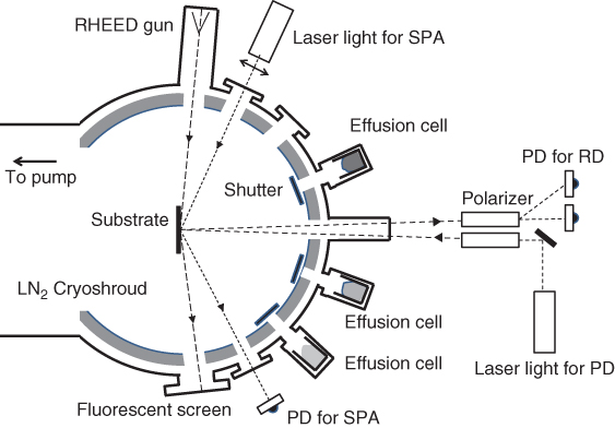
Figure 2.1 Schematic view of the growth chamber structure equipped with RHEED and optical diagnoses.
Growth initiation and termination are done by opening and closing the shutters set in front of the effusion cells, as shown in Figure 2.1. The performance of shutters is quite important to produce fine‐layer structures. The shutter action is completed by the mechanical movement of shutters. Although the growth rate of MBE is rather small compared with other growth methods such as liquid‐phase epitaxy (LPE) [15] and vapor‐phase epitaxy (VPE) [16], a quick shutter motion is required to achieve fine growth control with monolayer accuracy. Nevertheless, the movement of shutters should be calm and smooth enough not to produce dust, which may attack the substrate surface. The lifetime of shutters is also important, because the growth of fine‐layer structures sometimes needs a large number of shutter actions. In modern MBE systems, the shutters of effusion cells are designed to fulfill the above prerequisites. Several mechanisms have been adopted for actuating the shutters: linear‐motion blade, rotating blade, and round lid system.
In Figure 2.1, geometrical setups of in‐situ observation tools are shown. They are reflection high‐energy electron diffraction (RHEED) [8,9] and optical diagnostic methods such as reflectance difference spectroscopy (RDS) [17] and the surface photoabsorption method (SPA) [18]. These will be discussed later.
2.3 Atomic and Molecular Beam Sources
Atomic/molecular beams are supplied from effusion cells. There are several ways to establish stable atomic/molecular beams. The most important one is to employ an effusion cell with electrically heated crucible. The source material in a crucible is solid and heated to yield the required vapor pressure. This type of MBE is usually called solid‐source MBE. Before growth, effusion cells with empty crucibles are carefully baked at sufficiently high temperatures in order to remove adsorbed atoms and molecules. This process helps to keep the purity of the molecular beam, even when the molecular beam intensity is very low. Various materials are used for crucibles: pyrolytic boron nitride (pBN), fused quartz, high‐melting‐point metals, graphite, and so on. High‐purity pBN is often used when the evaporation temperature is less than approximately 1200 °C, because pBN is quite stable both thermally and chemically. For source materials which need higher evaporation temperatures, high‐melting‐point metals such as tungsten (W), platinum (Pt), and tantalum (Ta) are used, depending on the chemical properties of source materials. A fused quartz crucible is sometimes employed for relatively low‐temperature evaporation materials, and for organic source materials. For the evaporation of refractory metals and metal oxides, very high temperatures are required. In such cases, electron beam (e‐beam) heating is often used. By focusing the e‐beam on the source material surface, only a small part of the source material can be heated. Therefore, the crucible can stay at relatively low temperatures. As a result, very pure atomic or molecular beams are created.
In MBE growth using solid sources, molecular beam intensities are controlled by the temperature of the source material (i.e. the temperature of the crucible). The evaluation of emission intensities from the effusion cells is well established, based on ideal Knudsen effusion cells (K‐cells) [ 1,19]. In the ideal K‐cell, thermodynamic equilibrium should be established between the source material and its vapor pressure. The ideal K‐cell should have an opening much smaller than the mean free path of the molecules in the cell. The opening should also be much smaller than the surface area of the source material in the cell. The thickness of the opening should be negligibly small. In other words, there is no wall in the opening [ 1, 19]. The structure of an ideal K‐cell is shown schematically in Figure 2.2. With all these K‐cell conditions, the total number of molecules emitted from the K‐cell opening per second is expressed by the following equation [1]:

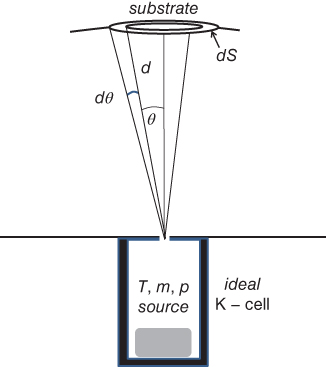
Figure 2.2 Schematic view of the ideal K‐cell.
where m and T denote the molecular weight and temperature in the K‐cell, p indicates the equilibrium pressure in the ideal K‐cell, and s0 is the opening area of the cell. The beam intensity on the substrate surface can be estimated by considering the fact that the emission from the ideal K‐cell follows a “cosine law.” By using the beam intensity impinging on a small area dS subtended by the solid angle dω (between θ and θ + dθ) in Figure 2.2, the beam intensity per unit area of the substrate will be given as:

where d indicates the distance from the opening of the K‐cell to the substrate surface. Je in Eq. 2.2 is determined solely by the K‐cell temperature. Since p denotes the equilibrium pressure in the cell and is expressed as p = nkT, Eq. 2.2 can be expressed as:

However, the molecular beam intensity given by Eq. 2.3 is so small that very high crucible temperatures are needed to achieve reasonable growth rates. In practical MBE growth, therefore, modified K‐cell structures are adopted, where crucibles have large openings. The crucible structure is shown schematically in Figure 2.3. Figure 2.3(a) shows the ideal K‐cell structure with a minimal opening. For the modified K‐cells, the effect of the crucible shape, cylindrical and conical shaped walls, has been investigated on the beam uniformity around the substrate surface [20,21]. In any case, the angular distribution of effusion no longer follows the cosine law, but has a more directional shape against the substrate, as shown in Figure 2.3(b). In addition, in the modified K‐cell structure, the equilibrium pressure will not be established in the crucible. The molecular beam intensity depends not only on the cell temperature, but also on the shape of the crucible opening. The molecular beam intensity is also affected by the surface area of the remaining source material. Therefore, it is not easy to predict the molecular beam intensity by the cell temperature and the geometrical configuration of the cell. Instead, the molecular beam intensity is estimated in practice by measuring the beam equivalent pressure (BEP) using a vacuum gauge set at the substrate position. The measurement of the molecular beam intensity will be discussed later.
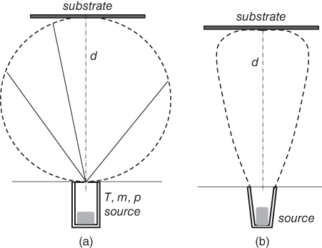
Figure 2.3 Angular emission patterns for ideal K‐cell (a) and modified K‐cell (b).
In addition to the solid‐source effusion cells discussed above, gas‐source effusion cells are also used in MBE. Source gases are introduced from outside the MBE system through UHV valves and a mass flow controller. Therefore, no material exhaustion takes place and continuous long‐term MBE operation could be achieved. A variety of source gases, such as metal‐organic compound gases and hydrides, are used. Metal‐organic compound molecules are usually supplied directly to the heated substrates, while hydrides are sometimes thermally cracked through cracker cells. The MBE system using metal‐organic compound sources is often called metal‐organic MBE (MOMBE) [22]. When hydrides are used for source materials, this is called gas‐source MBE (GSMBE) [23]. The MBE method which uses both metal‐organic compound sources and hydride sources is sometimes called chemical beam epitaxy (CBE) [24]. The molecular beam intensity of these gaseous source cells can be estimated by mass flow controllers. The mass flow controller data indicate the total number of molecules emitted from the effusion cell. The density per unit area on the substrate surface could be determined by considering the structure of the effusion cells.
The growth of III‐nitrides by metal‐organic vapor‐phase epitaxy (MOVPE) and MBE has attracted much attention in the last two decades for device applications. Growth by MBE needs efficient molecular sources of nitrogen. Since the nitrogen molecule (N2) is quite stable, no efficient decomposition of N2 molecules occurs on the substrate surface. Instead, NH3 molecules are supplied on the heated substrate surface. With this method, successful growth of GaN and AlGaN has been achieved [25]. Alternative methods to supply active N atoms on the surface have been developed, mainly to improve the growth rate. These employ plasma to excite N2 gas, producing either atomic N or excited N2 molecules. This is called plasma‐assisted MBE (PAMBE) or plasma‐enhanced MBE (PEMBE) [26,27]. Plasma‐assisted effusion cells with high dissociation efficiency are now commercially available, and are considered to be standard equipment for MBE growth of III‐nitride materials.
Metal oxides have been paid considerable attention for their optical applications. Although oxygen molecules are a little less stable compared with nitrogen molecules, the incorporation rates into the oxides are very poor. Therefore, much more active species – such as atomic and excited oxygen molecules – are needed. As with the growth of nitrides, radio frequency (RF) plasma‐assisted effusion cells are used for the growth of oxides. Among the metal oxides, ZnO is one of the most attractive materials because of its optical properties. ZnO films have been grown by MBE using RF plasma‐assisted effusion cells [28]. For the growth of nitrides and oxides using plasma‐assisted effusion cells, pure N2 or O2 gas is supplied from outside through a UHV valve and a mass flow controller. Therefore, the density of excited particles cannot be measured directly.
2.4 Measurement of MBE Growth Parameters
The important parameters needed to operate an MBE system include those related to background atmospheric conditions, substrate temperature, and atomic/molecular beam intensity. These are listed in Figure 2.4.
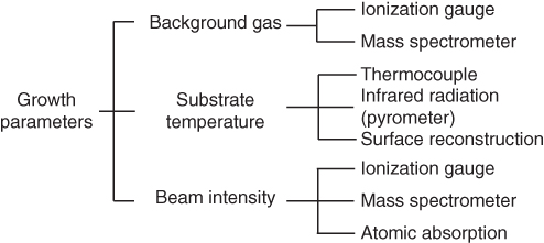
Figure 2.4 Growth parameters needed for MBE growth.
The background atmospheric conditions are quite important in MBE, because extremely low background pressure is inevitable for the growth of high‐purity material and interfaces. Gaseous species in the residual gas are also important. The existence of reactive gases such as CO, O, and H2O is quite harmful. In MOVPE, the substrate temperature is very close to that of the carbon substrate holder, because H2 molecules transfer heat to the substrate efficiently. However, in MBE, where no such heat‐conducting species exist, the temperature gap between the substrate and the substrate holder is not small. Therefore, correct temperature measurement is very difficult.
2.4.1 Measurement of Background Atmospheric Conditions
Residual gases in the MBE chambers usually come from the inner surface of the chamber, mainly caused by incomplete baking before starting the MBE operation. Undesirable gas molecules also come from the heated components in the chamber, such as effusion cells, substrate holder, and shutter blades heated by effusion cells. Sufficient degassing is needed from these components before growth. The amount of residual gas is measured by ionization gauges, while gaseous species and their quantities are detected by mass spectrometer. A quadrupole mass spectrometer (QMS) is used for this purpose, because of its compactness and stability. Residual gases such as H2O, CO, CO2, and O2 are often observed in the mass spectrum. Although their detected intensities are much less than 10−11 Å level, oxygen and carbon are incorporated into the grown semiconductor layers as impurities, because they react easily at the heated substrate surface. Thus, lowering the amount of residual gases is very important to produce high‐purity materials.
2.4.2 Measurement of Substrate Temperature
Accurate measurement of the substrate temperature is necessary to establish proper growth conditions. The substrate temperature is usually measured by a thermocouple set behind the substrate holder. Since the substrate holder is usually designed to be rotatable around the central axis, however, the thermocouple cannot be set firmly on the holder. Therefore, the measured temperatures of the substrate holder are different from the true ones. Sometimes the temperature difference between them is higher than 100 °C.
In addition, the temperature gap between the holder and the substrate set on it is not small. To minimize this gap, substrates are often mounted firmly on the holder using In solder.
Substrate temperature can be monitored more accurately using a pyrometer, where the substrate temperature is evaluated by the infrared light intensity emitted from the heated substrate surface. Therefore, temperature measurement by pyrometer requires a proper value of the emissivity of the substrate surface. Since a pyrometer requires only a transparent window on the chamber, it is useful to apply to MBE. However, since the temperature is evaluated by the light intensity in a specific wavelength, the window should be kept clean so as not to deteriorate the transmitting light intensity. The light wavelength used in a narrow‐band pyrometer is a specific one in the range 0.7–20 µm. A pyrometer with wavelength opaque to the substrate material provides information from the substrate. Otherwise, the pyrometer measures the temperature of the substrate holder surface behind the substrate. In addition, the temperature as measured by pyrometer is affected by radiation from the effusion cells. Therefore, accurate temperature measurement is not easy in either thermocouple or pyrometer.
The measured temperatures are, therefore, often calibrated using other measures, such as the melting point of metals, intermetallic alloying temperature, and the change of surface reconstruction of the substrate surface. Al (melting point 660.4 °C) and GaSb (665 °C) are often used. The eutectic point between Si and Al (577 °C) is also used by evaporating Al on a Si substrate.
However, these methods are applicable only once, and cannot be used repeatedly. Temperature estimation through the phase change of the surface reconstruction can be used in MBE growth with a GaAs substrate. On the (001) GaAs surface, arsenic coverage depends on the temperature and different reconstructions appear under different arsenic coverages. The reconstruction change can be detected by RHEED pattern observation. Below the congruent sublimation temperature, As is accumulated on the (001) surface and a (2 × 4) As stable surface is established. As the temperature increases, As2 molecules are evaporated and the surface reconstruction changes from a (2 × 4) to a (4 × 2) Ga stable surface through the intermediate structure of (3 × 1). Although this transition occurs at the congruent sublimation temperature in vacuum, the temperature will be changed because of the existence of residual As pressure in the MBE chamber. Therefore, the relationship between the transition temperature and As pressure should be established. The (3 × 1) to (4 × 2) transition temperature at various As pressures was measured and used to determine the substrate temperature [29]. With this method, however, the accuracy of temperature measurement remains ±5 °C. This is probably caused by the fact that the phase transition from (3 × 1) to (4 × 2) is a higher‐order transition, where the transition occurs rather mildly [30]. When (001) InAs is used instead of GaAs, much higher accuracy is expected because the (2 × 4) to (4 × 2) transition on (001) InAs is a first‐order transition [31].
2.4.3 Measurement of Atomic/Molecular Beam Intensity
Measurement of the effusion rates is quite important because it determines the growth rates. As discussed previously, the effusion rate from an ideal K‐cell is determined by the cell temperature and corresponding equilibrium vapor pressure in the cell. However, the atomic or molecular beam intensity from an ideal K‐cell is very weak. Therefore, modified K‐cells with wide openings are used instead of ideal K‐cells. In a modified K‐cell, an equilibrium vapor pressure cannot be established in the crucible with a given temperature. Thus, the effusion rate from the modified K‐cell depends not only on the cell temperature but also on the amount and the surface area of the source material. The latter varies with time and is not easily predicted.
Therefore, to determine the atomic/molecular beam intensity, direct measurement of beam intensity is often adopted using an ionization gauge placed at the substrate position. The measured value is called the BEP. As discussed in Section 2.3, the atomic/molecular beam intensity is given by Eq. 2.3 for an ideal K‐cell. The value ![]() is proportional to the number of molecules on the substrate, and will be related to the BEP. Thus, the relationship will be expressed as:
is proportional to the number of molecules on the substrate, and will be related to the BEP. Thus, the relationship will be expressed as:
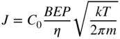
In this equation, C0 is a proportional constant and η is the ionization efficiency of the source molecules. If the molecular beam intensity and the corresponding BEP are available for a particular material, then the molecular beam intensity of the other materials can be estimated using the following equation [32]:

Here, Ga is used as a standard material because, as described later, the atomic beam intensity of Ga can be determined accurately by the use of RHEED observation. In Eq. 2.5, JGa, BEPGa, TGa, and mGa denote the data on Ga, while Ji, BEPi, Ti, and mi are for an arbitrary material. They represent the beam intensity, BEP, cell temperature, and molecular or atomic mass. ηGa and ηi are the ionization efficiency of Ga and the other material i relative to that of the nitrogen molecule, according to:

where Z is the atomic number [33]. The estimation of η could deviate from Eq. 2.6, depending on the shape of the molecules. If the molecules are decomposed in the ionization gauge by electron impact, then η deviates from Eq. 2.6. However, most of the solid‐source materials for III–V and II–VI growth follow the above equation.
Other methods, such as mass analysis and atomic absorption spectroscopy, are also applicable to estimate the atomic and molecular beam intensity. QMS can detect the kind and number of molecules at the same time, if the detector portion is exposed to the atomic or molecular beams. However, the sensitivity of the detector could be deteriorated by deposited materials, and therefore a QMS is set in the shadow of the beams and usually used for residual gas analysis.
Another sensitive method is atomic absorption spectroscopy [34]. This method is used for the quantitative determination of chemical elements by using the absorption of optical radiation from a hollow‐cathode lamp. A hollow‐cathode lamp is a type of discharge lamp that produces narrow emission lines inherent to the atomic species of the cathode material. By using absorption of this light, the density of atoms in the vapor can be evaluated. Although this method requires a hollow‐cathode lamp with the same cathode material as the material to be measured, it can be done without ceasing the growth. However, this method is applicable only to atomic sources. For molecular source materials, this method cannot be applied.
2.5 Surface Characterization Tools for MBE Growth
MBE growth proceeds under local thermal equilibrium in the vicinity of the substrate surface. This makes a sharp contrast with other growth methods such as LPE [35,36] and VPE [ 16,37], where thermal equilibrium between source material and substrate is a fundamental requisite. Since MBE growth is performed in UHV conditions, events on the growing surface can be investigated precisely using electron beam, ion beam, and optical means. Therefore, MBE growth processes on particular materials are well understood compared with other growth methods such as LPE and MOVPE. In this section, surface observation tools applicable to MBE are discussed; these are listed in Figure 2.5. As shown, there are two categories of surface evaluation methods: “in‐situ” methods (i.e. those which are applicable without ceasing growth) and others that require growth interruption for measurements and are often carried out in neighboring or external chambers. The latter include secondary ion mass spectrometry (SIMS), AES, XPS, ultraviolet photoemission spectroscopy (UPS), and scanning tunneling microscopy (STM). These are useful surface analysis tools. Among these methods, STM is often combined with the MBE system and used to investigate the atomic behavior on the substrate. However, these methods will not be discussed any further here. Instead, we devote ourselves to the “in‐situ” evaluation methods. Since MBE growth occurs in a UHV environment, various probes such as electrons, ions, and photons are applicable. Among the “in‐situ” evaluation methods in Figure 2.5, we will concentrate on RHEED observation and optical diagnostic methods such as RDS [17] and SPA [18], because they are most easily equipped in the MBE growth chamber, as shown in Figure 2.1.
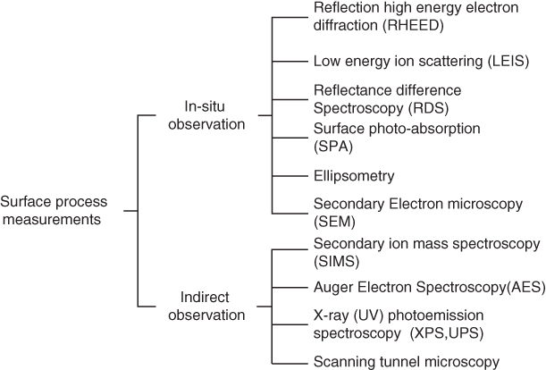
Figure 2.5 Surface characterization tools for MBE growth.
In Figure 2.5, however, low‐energy ion scattering (LEIS) and secondary electron microscopy (SEM) are also categorized as “in‐situ” methods. Although these methods are not popular for controlling the growth process, they provide useful information on the surface atomic configuration and microstructures. In LEIS measurement, the system designed for MBE is used. This system is called coaxial impact collision ion scattering spectroscopy (CAICISS) [38,39], where a reflected beam is detected at the same position as the incident He+ beam source. Therefore, the measurement is completed by only one port of the chamber. In CAICISS, He ions accelerated to 1–3 keV are irradiated on the substrate surface. After head‐on collision with the surface atoms, reflected ions are detected by a micro channel plate (MCP), and their energy and time delay after collision are measured. The important point of this measurement is that the resulting data reflect real‐space information. Note that RHEED provides reciprocal lattice information.
As with LEIS, SEM also provides real‐space surface images. Therefore, it is useful to understand the surface process during growth [40]. In SEM measurements in MBE, the electron gun system of a scanning electron microscope is set on the MBE chamber. Since, in SEM measurements, secondary electrons excited by e‐beam are collected by the detector, no Bragg angle condition is necessary. Therefore, the incident e‐beam can be focused as sharply as possible and there is no restriction on the incident angle.
As a result, high‐resolution surface images are provided [41,42]. Indeed, step motion and island formation processes during growth have been demonstrated.
2.5.1 Reflection High‐Energy Electron Diffraction
A modern MBE system is equipped with a RHEED system. RHEED produces an e‐beam accelerated by a voltage of 10–50 keV. For high‐energy e‐beams, the scattering cross‐section on the substrate surface decreases quickly with increasing incident angle. Therefore, the e‐beam incident angle (θ) should be less than ∼5° with respect to the substrate surface, as shown schematically in Figure 2.6. Instead, the impinging molecular beams are hardly influenced by RHEED observation. The e‐beam reflected on the substrate surface is focused on the fluorescent screen. The wavelength of the e‐beam is given by the following equation [43] (with the above acceleration voltages, λ ranges from 0.12 to 0.06 Å):
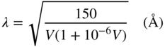

Figure 2.6 Diffraction condition of the incident e‐beam on the substrate surface.
Even with a shallow angle of incidence, the e‐beam can penetrate deep into the crystal from the surface. However, because of the intense inelastic scattering in the crystal, elastic scattering takes place only in a few monolayers from the substrate surface. In other words, the diffracted e‐beam involves information of a few surface monolayers [44]. Indeed, the interference depth of electrons in an Al single crystal is only 0.5 nm when the acceleration voltage is 10 keV and the incident angle is 2°. Therefore, RHEED is extremely surface sensitive. On the other hand, the lateral interference length is mainly determined by the convergence angle of the e‐beam. If it is 1 mrad and the acceleration voltage is 15 keV, the lateral interference length will be approximately 140 nm when the incident angle is 2°.
In RHEED, the diffraction condition is given by the following equation:
where k0 and k1, respectively, denote the wave vectors of the incident and diffracted e‐beam. Since the energy loss in the diffraction process is negligibly small, the diffraction condition of Eq. 2.8 can be given by the intersection point of a Ewald sphere (with radius |k0|) and the reciprocal lattice point. In the RHEED observation, diffraction occurs only in a very thin surface layer, as discussed above. Therefore, the lattice lacks periodicity in the vertical direction, and behaves as a 2D lattice. The corresponding reciprocal lattice forms a 1D rod array in the vertical direction of the crystal lattice surface. Figure 2.6 shows schematically the diffraction condition in the RHEED observation. The radius of the Ewald sphere is much larger than the spacing of the reciprocal lattice. For an acceleration voltage of 10 kV, the radius ![]() while the spacing between the reciprocal lattice rods in the [110] principal axis on a (001) GaAs surface is
while the spacing between the reciprocal lattice rods in the [110] principal axis on a (001) GaAs surface is ![]() . Therefore, many diffraction spots appear on the fluorescent screen. The spot on the fluorescent screen reflects the intersection point of the Ewald sphere and the reciprocal lattice rod. Therefore, the spot should be small and sharp for ideal 2D lattices. In a practical system, the surface is covered with growth nuclei, small one‐monolayer steps, and other defects. As a result, the reciprocal lattice rods have finite thicknesses. Thus, the spots on the fluorescent screen will have a slightly thicker and vertically elongated shape. Therefore, the streaky‐shaped RHEED pattern reflects the surface unevenness discussed above.
. Therefore, many diffraction spots appear on the fluorescent screen. The spot on the fluorescent screen reflects the intersection point of the Ewald sphere and the reciprocal lattice rod. Therefore, the spot should be small and sharp for ideal 2D lattices. In a practical system, the surface is covered with growth nuclei, small one‐monolayer steps, and other defects. As a result, the reciprocal lattice rods have finite thicknesses. Thus, the spots on the fluorescent screen will have a slightly thicker and vertically elongated shape. Therefore, the streaky‐shaped RHEED pattern reflects the surface unevenness discussed above.
In addition to the surface unevenness, there exists a high density of dangling bonds on the surface. To minimize the increased surface energy by these dangling bonds, the surface bond structure is modified to create new pairs. This reconstruction results in new periodicity in the surface atomic bonding structure. New periodicity is superimposed on the original periodicity and observed on the RHEED fluorescent screen. The important structures are (2 × 4) and (4 × 2) on the GaAs (001) surface [9] and (7 × 7) on the Si (111) surface. (n × m) indicates the n times and m times periodicity with respect to the original lattice along the principal axes. Two‐times periodicity on the GaAs (001) surface is caused by As dimer formation in the [![]() ] direction, while four‐times periodicity is due to the As dimer missing in the [110] direction with this periodicity. The (7 × 7) structure on Si (111) is caused by the Si atom missing along the principal axes every seven original lattice points. These results have been confirmed by STM observation.
] direction, while four‐times periodicity is due to the As dimer missing in the [110] direction with this periodicity. The (7 × 7) structure on Si (111) is caused by the Si atom missing along the principal axes every seven original lattice points. These results have been confirmed by STM observation.
In addition to these static RHEED observations, the intensity of diffracted spots on the fluorescent screen has been found to oscillate during growth [45]. This oscillation is caused by the repetition of rough and flat surface formation. In the growth of GaAs and Si, the periodicity of oscillation was found to coincide exactly with the time needed to complete one‐monolayer growth. This oscillation is widely used to estimate the growth rate and molecular beam intensity of Ga and Si, because at the temperatures used in GaAs and Si growth, their sticking coefficients are almost one [46,47]. This phenomenon has been confirmed with many other materials.
2.5.2 Optical Diagnostic Methods
RHEED is the most commonly used surface‐sensitive diagnostic method in MBE. Indeed, RHEED provides useful information on surface structure as well as growth dynamics. RHEED requires UHV conditions because it uses an e‐beam as a probe. Therefore, application of RHEED may be difficult when the ambient pressure is raised in the case of plasma‐assisted MBE. In addition, a high‐energy e‐beam may produce damage on the surface. All these problems are circumvented by applying optical diagnostic methods. Optical methods are easily adopted because they need only one or two windows on the chamber. The most fundamental optical method is ellipsometry [48]. In this method, polarized light is irradiated on the surface and the polarization of reflected light is analyzed. This method enables us to determine the layer thickness and its optical constants at the same time. The information from the ellipsometry also includes data from the top surface where the growth takes place. However, this is easily masked by the dominant contribution from the bulk layer. Therefore, in order to obtain the data from the growth front by optical means, it is necessary to compensate for the contribution of the bulk layer.
RDS [17] and SPA [18] have been developed to remove the bulk effects from the optical data. In RDS, polarized light is irradiated vertically on the growing surface and reflected light is divided into two orthogonally polarized components with respect to the principal axis of the surface, as shown in Figure 2.7. In the growth on GaAs (001), the incident light will be polarized in the [010] direction. The reflected light polarized in [110] and ![]() directions is measured independently. The difference between them will give the surface signal. The bulk effect, which is considered to be isotropic, will be removed by taking the difference between these two components. The output of RDS is given by [49]:
directions is measured independently. The difference between them will give the surface signal. The bulk effect, which is considered to be isotropic, will be removed by taking the difference between these two components. The output of RDS is given by [49]:

![Schematic setup of the RDS measurement. The incident light passes through the polarizer and then bounces to the substrate (001) and passes through the analyzer. Arrows from the analyzer are labeled R[1-10] and R[110].](http://images-20200215.ebookreading.net/2/1/1/9781119355014/9781119355014__molecular-beam-epitaxy__9781119355014__images__c02f007.jpg)
Figure 2.7 Schematic setup of the RDS measurement.
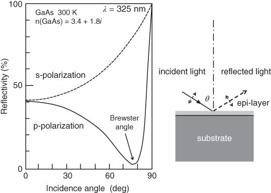
Figure 2.8 Principle of the SPA measurement using Brewster angle reflection.
where ![]() , λ is the wavelength used,
, λ is the wavelength used, ![]() is a dielectric constant of the substrate,
is a dielectric constant of the substrate, ![]() and
and ![]() are components of the dielectric constant. RDS has been applied to the growth of GaAs and AlGaAs on (001) GaAs substrate and compared with the results of RHEED observation. The RDS spectrum is found to be related to the surface reconstruction observed in RHEED [50]. SPA is another method to eliminate the effect of the substrate. In this method, p‐polarized light is irradiated on the substrate surface at the Brewster angle (θB), which will be given by the following equation:
are components of the dielectric constant. RDS has been applied to the growth of GaAs and AlGaAs on (001) GaAs substrate and compared with the results of RHEED observation. The RDS spectrum is found to be related to the surface reconstruction observed in RHEED [50]. SPA is another method to eliminate the effect of the substrate. In this method, p‐polarized light is irradiated on the substrate surface at the Brewster angle (θB), which will be given by the following equation:
In this equation, n denotes the refractive index of the grown material, while n0 is the refractive index of vacuum. For semiconductor materials, θB∼70∘. As shown in Figure 2.8, the reflectivity of incident light with p‐polarization almost disappears at the Brewster angle. The reflectivity change due to the surface layer of thickness d will be given by the following equations for s‐ and p‐polarized light [49]:

Here, λ is the wavelength of light used, ![]() and
and ![]() denote the dielectric constant of the growing layer and the substrate, respectively. The sensitivity of this method is demonstrated in Figure 2.9, where the reflectivity change by one‐monolayer of Ga on the GaAs (001) surface is calculated by these equations. For the light wavelength, λ = 325 nm and λ = 488 nm are used. The corresponding refractive indices of GaAs are n = 3.4 − 1.8i and n = 4.5 − 0.41i, respectively [51]. For the dielectric constants of the Ga monolayer, the values of bulk Ga are used. These are
denote the dielectric constant of the growing layer and the substrate, respectively. The sensitivity of this method is demonstrated in Figure 2.9, where the reflectivity change by one‐monolayer of Ga on the GaAs (001) surface is calculated by these equations. For the light wavelength, λ = 325 nm and λ = 488 nm are used. The corresponding refractive indices of GaAs are n = 3.4 − 1.8i and n = 4.5 − 0.41i, respectively [51]. For the dielectric constants of the Ga monolayer, the values of bulk Ga are used. These are ![]() and
and ![]() , respectively [52]. Figure 2.9 clearly shows that the sensitivity increases dramatically as the incident angle approaches the Brewster angle. Since the reflection from the bulk GaAs is minimized at the Brewster angle, high sensitivity can be achieved [53].
, respectively [52]. Figure 2.9 clearly shows that the sensitivity increases dramatically as the incident angle approaches the Brewster angle. Since the reflection from the bulk GaAs is minimized at the Brewster angle, high sensitivity can be achieved [53].
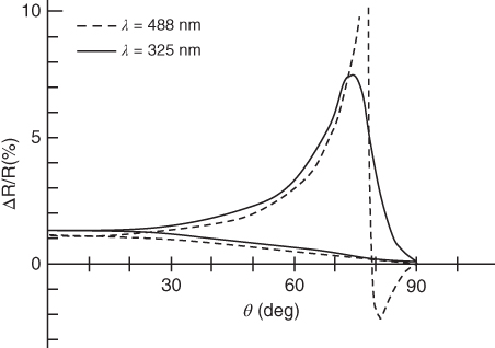
Figure 2.9 Sensitivity of SPA. The reflectivity change due to one‐monolayer Ga deposition on the GaAs substrate is shown as a function of incident angle for both s‐ and p‐polarized light.
In both methods, spectral responses are also obtained by changing the incident light wavelength. From the spectral response, the chemical information of the surface is obtained.
2.6 Summary
In this chapter, the fundamental setup of a MBE system has been discussed. Nowadays, MBE systems are used in a wide range of applications, from fundamental research to production areas. Understanding of the growth mechanism of MBE has progressed over the last two decades, through observations by RHEED and other surface diagnostic tools. In addition, the quality of MBE chambers and other accessories, such as effusion cell systems in particular, has also improved considerably. As a result, modern MBE machines have the capability to produce high‐quality material layers with extremely high thickness control and long‐term stability. Because of this characteristic, quantum cascade lasers and quantum dot lasers have been fabricated.
MBE is now being applied to develop new devices and pursue new phenomena based on quantum dots and quantum wires using a variety of materials. For these applications, appropriate surface diagnostic methods are necessary. As with the RHEED method, the optical means discussed in this chapter will be useful because no additional setup is needed for these measurements. In addition, information from the chemical bonding of the surface is available in the optical methods.
Acknowledgments
The author would like to acknowledge A. Kawaharazuka and J. Nishinaga for their support and suggestions throughout this work. This work is partly supported by a Grant‐in‐Aid for Scientific Research (A) from the Japan Society for the Promotion of Science (JSPS) and the COE Program “Molecular Nanoengineering,” from the Ministry of Education, Culture, Sports, Science and Technology (MEXT), Japan.
References
- 1 Herman, M.A. and Sitter, H. (1988). Molecular Beam Epitaxy; Fundamentals and Current Status. New York: Springer.
- 2 Parker, E.H.C. (ed.) (1985). The Technology and Physics of Molecular Beam Epitaxy. New York: Plenum.
- 3 Henini, M. (2012). Molecular Beam Epitaxy; From Research to Mass Production. Amsterdam: Elsevier.
- 4 Arthur, J.R. (1968). J. Appl. Phys. 39: 4032.
- 5 Arthur, J.R. and LePole, J.J. (1969). J. Vac. Sci. Technol. 6: 545.
- 6 A.Y. Cho, M.B. Panish, and I. Hayashi, Proceedings of the Third International Symposium on GaAs and Related Compounds, Institute of Physics, London, vol. 18 (1970).
- 7 Cho, A.Y. (1971). J. Vac, Sci. Technol. 8: 531.
- 8 Cho, A.Y. (1970). J. Appl. Phys. 41: 2780.
- 9 Cho, A.Y. (1971). J. Appl. Phys. 42: 2074.
- 10 Cho, A.Y. and Arthur, J.R. (1975). Prog. Solid State Chem. 10: 157.
- 11 Joyce, B.A. (1968). J. Cryst. Growth 3: 43.
- 12 Joyce, B.A. (1974). Rep. Prog. Phys. 37: 363.
- 13 Davey, J.E. and Pankey, T. (1968). J. Appl. Phys. 39: 1941.
- 14 Saku, T., Hirayama, Y., and Horikoshi, Y. (1991). Jpn. J. Appl. Phys. 30: 902.
- 15 Miller, B.I., Pinkas, E., Hayashi, I., and Capik, R.J. (1972). J. Appl. Phys. 43: 2817.
- 16 Tietjen, J.J. and Amick, J.A. (1966). J. Electrochem. Soc. 113: 723.
- 17 Aspnes, D.E., Harbison, J.P., Studna, A.A., and Florez, L.T. (1987). Phys. Rev. Lett. 59: 1687.
- 18 Kobayashi, N. and Horikoshi, Y. (1990). Jpn. J. Appl. Phys. 29: 334.
- 19 Knudsen, M. (1915). Ann. Phys. 48: 1113.
- 20 Curless, J.A. (1985). J. Vac. Sci. Technol. B3: 531.
- 21 Yamashita, T., Tomita, T., and Sakurai, T. (1987). Jpn. J. Appl. Phys. 26: 1192.
- 22 Tokumitsu, E., Kudow, Y., Konagai, M., and Takahashi, K. (1984). J. Appl. Phys. 55: 3163.
- 23 Morris, F.J. and Fukui, H. (1974). J. Vac. Sci. Technol. 11: 506.
- 24 Tsang, W.T. (1974). J. Vac. Sci. Technol. B3: 666.
- 25 Yoshida, S., Misawa, S., and Gonda, S. (1982). J. Appl. Phys. 53: 6844.
- 26 Sato, Y. and Sato, S. (1989). Jpn. J. Appl. Phys. 28: L1641.
- 27 Paisley, M.J., Sitar, Z., Posthill, J.B., and Davis, R.F. (1989). J. Vac. Sci. Technol. A47: 701.
- 28 Fons, P., Iwata, K., Yamada, A. et al. (2000). Appl. Phys. Lett. 77: 1801.
- 29 Lamberg, L.P., Westin, J., and Andersson, T.G. (1987). J. Vac. Sci. Technol. B35: 1654.
- 30 Yamaguchi, H. and Horikoshi, Y. (1992). Appl. Surf. Sci. 60/61: 224.
- 31 Yamaguchi, H. and Horikoshi, Y. (1993). Phys. Rev. Lett. 70: 1299.
- 32 Wood, C.E.C., Desimone, D., Singer, K., and Wicks, W. (1982). J. Appl. Phys. 53: 4230.
- 33 Flaim, T.A. and Ownby, P.E. (1971). J. Vac. Sci. Technol. 8: 661.
- 34 Kometani, T.Y. and Wiegman, W. (1975). J. Vac. Sci. Technol. 12: 933.
- 35 Panish, M.B. (1974). J. Cryst. Growth 27: 6.
- 36 Casey, H.C. Jr., Panish, M.B., Schlosser, W.O., and Paoli, T.L. (1974). J. Appl. Phys. 45: 322.
- 37 Boucher, A. and Hollan, L. (1970). J. Electrochem. Soc. 117: 932.
- 38 Katayama, M., Nomura, E., Kanekawa, N. et al. (1988). Nucl. Instrum. Methods Phys. Res. B33: 857.
- 39 Kudo, M. and Narusawa, T. (1990). J. Vac. Sci. Technol. B8: 697.
- 40 Inoue, N. (1991). J. Cryst. Growth 111: 75.
- 41 Inoue, N., Tanimoto, M., Kanisawa, K. et al. (1993). J. Cryst. Growth 127: 956.
- 42 H. Yamaguchi, Y. Homma, and Y. Horikoshi, Proceedings of the Third International Symposium on Atomic Layer Epitaxy and Related Surface Processes, May (1994).
- 43 Bauer, E. (1969). Techniques of Material Research, vol. 2 (ed. R.F. Bunshah). New York, Chapter 15: Wiley Interscience.
- 44 Ashley, J.C., Tung, C.J., and Ritchie, R.H. (1979). Surf. Sci. 81: 409.
- 45 Harris, J.J., Joyce, B.A., and Dobson, P.J. (1981). Surf. Sci. 103: L90.
- 46 Neave, J.H. and Joyce, B.A. (1983). Appl. Phys. A31: 1.
- 47 Horikoshi, Y., Yamaguchi, H., Briones, F., and Kawashima, M. (1990). J. Cryst. Growth 105: 326.
- 48 Fujiwara, H. and Kondo, M. (2005). Phys. Rev. B71: 075109.
- 49 McIntyre, J.D.E. and Aspnes, D.E. (1971). Surf. Sci. 24: 417.
- 50 Aspnes, D.E., Bhat, R., Caneau, C. et al. (1992). J. Cryst. Growth 120: 71.
- 51 Seraphin, B.O. and Benett, H.E. (1996). Semiconductors and Semimetals, vol. 3 (ed. R.K. Willardson and A.C. Beer), 519. New York: Academic Press.
- 52 Hunderi, O. and Ryderg, R. (1974). J. Phys. F: Met. Phys. 4: 2084.
- 53 Horikoshi, Y., Kawashima, M., and Kobayashi, N. (1991). J. Cryst. Growth 111: 200.