4
Nanostructure Formation Process of MBE
Koichi Yamaguchi
Department of Engineering Science, The University of Electro‐Communications, Tokyo, 182‐8585, Japan
4.1 Introduction
Recent progress in semiconductor epitaxial growth techniques, such as molecular beam epitaxy (MBE) and metal‐organic chemical vapor deposition (MOCVD), has enabled the fabrication of semiconductor nanostructures having low‐dimensional electronic characteristics. When the semiconductor crystal size is reduced to the de Broglie wavelength, electrons in the crystal have discretized density of states. In addition, since the degree of freedom of their movement is extremely limited, their kinetic energy increases. Therefore, as the crystal size decreases, the band‐gap energy increases. Owing to this quantum size effect, the absorption and emission wavelengths of light can be controlled by adjusting the semiconductor crystal size.
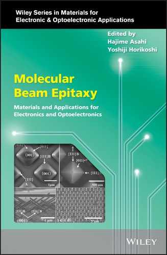
Figure 4.1 illustrates the density of states in the conduction bands of a bulk semiconductor, quantum well (QW), quantum well wire (QWR), and quantum dot (QD). The density of states for QW, QWR, and QD show, respectively, step, sawtooth, and delta functions. Semiconductor materials having low‐dimensional electronic characteristics are expected to enable the development of high‐performance optoelectronic devices. The thickness of the epitaxial layer can be controlled atomically by conventional MBE growth. Many QW devices have already been developed and put to practical use, such as semiconductor lasers. In addition, various special growth techniques of well‐controlled QWR, nanowire (NWR), and QD structures have been attempted so far. This chapter focuses on the basic growth processes of QW (Section 4.2), QWR and NWR (Section 4.3), and QD (Section 4.4) structures, based on MBE.
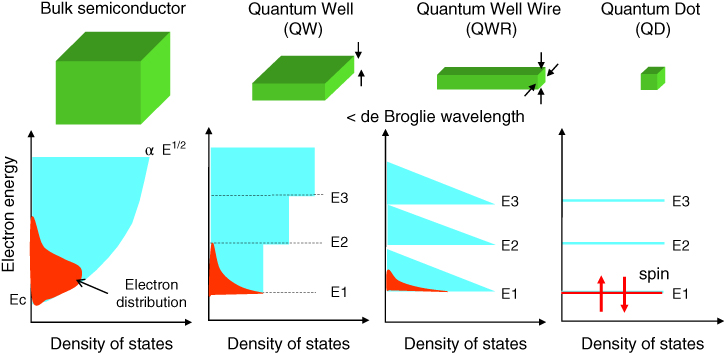
Figure 4.1 Schematics of the density of states of the conduction bands of a bulk semiconductor, QW, QWR, and QD.
4.2 Growth of Quantum Wells
QW structures showing the one‐dimensional (1D) quantum confinement effect are typically fabricated by heteroepitaxial growth on substrates. Thus, in order to fabricate QW structures, it is necessary to control the thickness of heteroepitaxial layers at the atomic level and to improve the flatness of the heterointerface. In MBE growth, reflection high‐energy electron beam diffraction (RHEED) is a powerful tool for controlling the epitaxial layer thickness. Since the RHEED specular beam intensity depends on the surface roughness at the atomic level, the intensity variation provides information about monolayer (ML) coverage during MBE growth [1].
In layer‐by‐layer growth through alternating repetitions of the step flow mode and two‐dimensional (2D) nucleation mode, the specular beam intensity usually oscillates, as shown in Figure 4.2. One cycle of specular beam intensity oscillation corresponds to a thickness of 1 ML. Thus, it is possible to control the growth of each monolayer. However, as conventional MBE growth progresses, the amplitude of the intensity oscillation gradually decays. This means that 2D nuclei are formed on the terrace before the monolayer is complete (i.e. multi‐nucleation‐mode growth occurs).
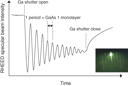
Figure 4.2 RHEED specular beam intensity as a function of GaAs growth time. The inset is a RHEED pattern obtained during growth.
Growth interruption is one useful technique for improving the surface flatness [2]. In Figure 4.2, the specular beam intensity increases with increasing growth interruption time because of the migration and rearrangement of surface atoms during growth interruption. Thus, a flat heterointerface structure can be obtained by growth interruption. However, it should be noted that impurities are incorporated into the heterointerface when the growth interruption time is prolonged. Figure 4.3 shows cross‐sectional transmission electron microscopy (TEM) images of well‐controlled InGaAs double QWs (27 ML) (a) and a GaAsSb single QW (3 ML) (b) in a GaAs matrix.
Figure 4.3 Cross‐sectional TEM images of InGaAs double QWs (27 ML) (a) and GaAsSb single QW (3 ML) (b).
In step‐flow‐mode growth on an off‐angle surface, specular beam intensity oscillations are often not observed [3]. When the terrace width is small (large off‐angle), only step‐flow growth occurs, and 2D nucleation on the terrace is suppressed. As a result, the specular beam intensity does not fluctuate during growth. A vertical heterointerface can be fabricated by preparing a uniform terrace width and precisely controlling sub‐monolayer growth by step‐flow‐mode growth. In particular, a vertical superlattice structure (SLS) can be fabricated by this growth technique [4], as shown in Figure 4.4.
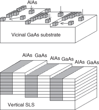
Figure 4.4 Schematics of growth process of a vertical GaAs/AlAs SLS on vicinal GaAs substrate.
When the QW thickness is less than 1 ML, many 2D islands are included in the QW layer. Scanning tunneling microscopy (STM) reveals that the InAs 2D islands formed by sub‐monolayer growth on GaAs(001) have an anisotropic shape extending along the ![]() direction. This is caused by an anisotropic strain at the InAs/GaAs heterointerface. Such InAs sub‐monolayer QWs (SMQWs) in a GaAs matrix show very sharp photoluminescence (PL) spectra. As the thickness of InAs SMQWs decreased from 1 to 1/12 ML, the PL peak energy at 10 K shifted from 1.4635 to 1.5118 eV, and the full‐width at half‐maximum (FWHM) decreased from 9.5 to 0.4 meV [5].
direction. This is caused by an anisotropic strain at the InAs/GaAs heterointerface. Such InAs sub‐monolayer QWs (SMQWs) in a GaAs matrix show very sharp photoluminescence (PL) spectra. As the thickness of InAs SMQWs decreased from 1 to 1/12 ML, the PL peak energy at 10 K shifted from 1.4635 to 1.5118 eV, and the full‐width at half‐maximum (FWHM) decreased from 9.5 to 0.4 meV [5].
4.3 Growth of Quantum Wires and Nanowires
This section describes the growth processes of semiconductor QWRs and NWRs. QWRs exhibit a 2D quantum confinement effect that creates a 1D electron system. QWRs are often buried in epitaxial layers and aligned along the in‐plane direction [6]. In contrast, NWRs are built vertically or grown laterally on the substrate [7]. The size of NWRs is not small enough to show a quantum confinement effect. However, QWs and QDs can be fabricated in NWRs by heterostructure growth. NWRs are expected to lead to new nanodevices that exploit their structural features. Figure 4.5 illustrates three types of QWRs and two types of NWRs. The QWRs in Figures 4.5(a, b) are fabricated by epitaxial growth into V‐shaped grooves and on striped ridges. Another is grown on the stepped surface structures [Figure 4.5(c)]. NWRs are normally fabricated by vapor–liquid–solid (VLS) catalysis [Figure 4.5(d)] or selective‐area growth [Figure 4.5(e)]. All of these growth processes will be described below.

Figure 4.5 Schematics of three types of QWRs and two types of NWRs: QWRs grown in V‐shaped grooves (a), QWR grown on striped ridge (b), QWRs grown on stepped surface structure (c), NWRs formed by VLS catalysis (d), and NWRs formed by selective‐area growth (e).
Figure 4.6 illustrates the formation process of V‐shaped GaAs QWRs. A striped mask pattern of the photoresist film is formed along the ![]() direction on a GaAs(001) substrate. Next, V‐shaped grooves are fabricated by wet chemical etching, and (111)A facets appear on both sidewalls of the V‐grooves. The growth rate of GaAs on the (001) bottom surface is usually higher than that on the (111)A sidewall facets. Thus, V‐shaped GaAs QWRs can be fabricated in the grooves by growing an AlGaAs/GaAs heterostructure [8,9].
direction on a GaAs(001) substrate. Next, V‐shaped grooves are fabricated by wet chemical etching, and (111)A facets appear on both sidewalls of the V‐grooves. The growth rate of GaAs on the (001) bottom surface is usually higher than that on the (111)A sidewall facets. Thus, V‐shaped GaAs QWRs can be fabricated in the grooves by growing an AlGaAs/GaAs heterostructure [8,9].
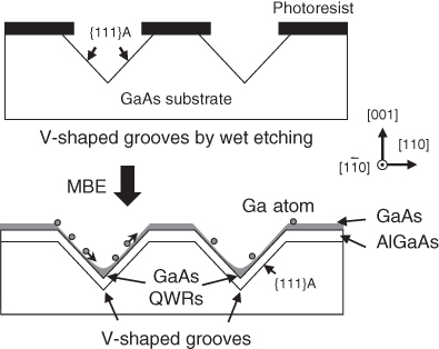
Figure 4.6 Schematics of growth process of V‐shaped GaAs QWRs.
Figure 4.7 illustrates the fabrication process of GaAs QWRs on top of sharp ridges. A striped ridge structure is formed along the [110] direction on a GaAs(001) substrate, and then a GaAs buffer layer is grown on this substrate. As the growth of GaAs proceeds, (111)B facets appear on both sidewalls of the ridged top layer [10]. The growth evolution of the ridge structure varies with growth competition on the (001) top surface and (111)B sidewall surface. As shown in Figure 4.8, the relationship between the growth rates of the (001) top surface (Rtop) and the (111)B sidewall surface (Rside) yield three types of top ridge shape. Rtop and Rside can be controlled by adjusting the growth conditions. If Rtop cos θ > Rside [Figure 4.8(a)], the width (W) of the (001) upper surface can be reduced to the quantum size. If Rtop cos θ = Rside [Figure 4.8(c)], the top width can be maintained constant. As a result, a GaAs QWR surrounded by the AlGaAs layer is formed on top of sharp ridges (Figure 4.7).
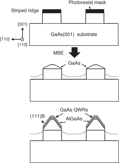
Figure 4.7 Schematics of fabrication process of GaAs QWRs on striped ridges.
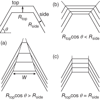
Figure 4.8 Growth evolution of ridge structures for three combinations of growth rates of (001) top surface (Rtop) and sidewall surface (Rside): Rtop cos θ > Rside (a), Rtop cos θ < Rside (b), and Rtop cos θ = Rside (c).
The large multi‐atomic steps and the sidewalls of a buffer layer serve as templates for the QWR growth. Figure 4.9 illustrates the formation process of multi‐atomic steps and QWRs on a buffer layer. In MOCVD, U‐shaped strip grooves are often prepared on the vicinal (001) GaAs substrate to increase the lengths of these QWRs. In a case of MBE, multi‐atomic steps are often formed on high‐index substrates [11,12]. Group III adatoms migrate on the terraces and are captured at up‐side or down‐side step sites. When the incorporation rate of adatoms at the down‐side step sites exceeds that at the up‐side step sites, step bunching occurs, and multi‐atomic steps are formed spontaneously. Therefore, long GaAs QWRs are grown at the edges of the multi‐atomic steps, and the resulting QWR layers can be stacked on the substrate (Figure 4.9).
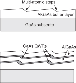
Figure 4.9 Schematic diagrams of formation process of GaAs QWRs formed at multi‐atomic step edges on a buffer layer.
Next, the fabrication process of III–V semiconductor NWRs is described. NWRs can be grown by bottom‐up techniques and are regularly fabricated using VLS growth [13] and selective‐area growth. Figure 4.10 illustrates two typical VLS growth methods for GaAs QWRs on Si substrates. One is Au‐assisted VLS growth [Figure 4.10(a)]. VLS growth of QWRs involves three distinct stages: alloying, nucleation and growth. First, Au droplets are prepared by deposition of a thin Au film and subsequent annealing. Then, Ga and As atoms are supplied and collected by the Au droplets. The solubility of As in the Au–Ga alloy droplets is very low, and there is no binary Au–As solid compound below 636 °C [14]. Supersaturation of the Au–Ga droplets leads to crystallization of the supplied species at the liquid–solid interface, and GaAs NWRs grow vertically [15].

Figure 4.10 Schematics of two typical VLS growth methods of GaAs QWRs on Si substrates: Au‐assisted VLS growth (a) and self‐assisted VLS growth (b).
The other VLS growth method illustrated in Figure 4.10 is self‐assisted VLS growth [Figure 4.10(b)]. Since the incorporation of Au into NWRs leads to scattering centers, Au‐free synthesis techniques have been investigated. One such technique currently used is Ga‐assisted VLS growth. GaAs NWRs can be fabricated using Ga droplets, formed by the Ga molecular beam of MBE [16]. This technique is called “self‐assisted VLS growth.” As shown in Figure 4.10(b), the supplied Ga atoms form the pinholes in a SiOx thin film prepared on a Si substrate. Then, Ga droplets are formed on the Si surface through the pinholes. Supersaturation of As‐containing Ga droplets leads to the crystallization of GaAs at the liquid–solid interface.
Owing to recent advances in lithographic techniques, selective‐area growth can be employed to fabricate NWR arrays with well‐controlled wire diameter and pitch [17]. Figure 4.11 illustrates the selective‐area‐growth process used for AlGaAs/GaAs NWRs on Si substrates. The nanosized opening pattern is fabricated in a SiOx mask film deposited on the substrate using lithography and etching techniques. The sticking coefficient of adatoms on the SiOx mask is lower than that on the exposed semiconductor surface of the opening region [Figure 4.11(a)]. In addition, surface diffusion of III‐adatoms occurs from the mask region to the opening region. Consequently, the GaAs NWRs are grown selectively from the opening region. Essentially, in the initial growth stage of NWR growth, the wire diameter is limited by the mask diameter [Figure 4.11(b)]. As the NWRs grow vertically, facets appear on the sidewalls. The layer‐by‐layer growth proceeds on the top surface and sidewalls, and the growth rates depend on the growth conditions. Thus, “core–shell” AlGaAs/GaAs heterostructures with the quantum confinement effect can be produced by controlling the growth conditions [Figure 4.11(c)].
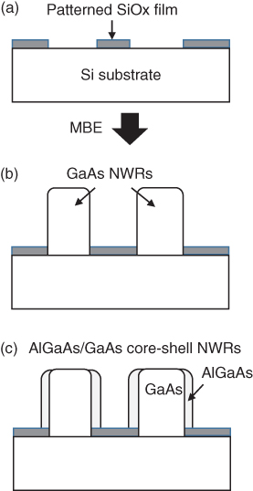
Figure 4.11 Schematics of selective‐area growth of AlGaAs/GaAs NWRs on Si substrate: SiOx mask film patterned on Si substrate (a), initial growth of GaAs NWRs on opening area (b), and AlGaAs/GaAs core–shell NWRs (c).
4.4 Growth of Quantum Dots
Semiconductor QDs have an atomic‐like density of states based on a zero‐dimensional (0D) quantum confinement effect. Hence, QDs are also referred to as “artificial atoms.” This and other attractive properties of QDs can presumably be exploited in various next‐generation optoelectronic devices. In order to develop QD devices, the QD structure must be precisely controlled. There are two main methods for growing self‐assembled QDs: the Stranski–Krastanov (SK)‐growth‐mode method [18] and the droplet‐epitaxy method [19]. In this section, SK growth of self‐assembled QDs is described.
Figure 4.12 illustrates the relationship between the growth amount and the free energy of 2D and 3D growth in the SK mode. A 2D–3D growth‐mode transition of SK growth is often observed in the heteroepitaxial growth of lattice‐mismatched materials. During the initial SK growth, the free energy of 2D growth is lower than that of 3D growth ([A]). As growth progresses, the strain energy increases. When the free‐energy relationship reverses owing to the increased strain, a growth‐mode transition from 2D to 3D growth occurs spontaneously ([B]). The resulting coherent 3D islands with high crystal quality [20] are often used as self‐assembled QDs. However, it should be noted that dislocations are formed in the case of excessive growth ([C, D]).
![Graph of free energy vs. growth amount for 2D and 3D growths in the SK mode, displaying 2 ascending curves passing through [A], [B], [C], and [D] regions. On the right are 4 schematics labeled [A], [B], [C], and [D].](http://images-20200215.ebookreading.net/2/1/1/9781119355014/9781119355014__molecular-beam-epitaxy__9781119355014__images__c04f012.jpg)
Figure 4.12 Free energy vs. growth amount for 2D and 3D growth in the SK mode.
In MBE, RHEED monitoring is a useful tool to control growth. Figure 4.13 shows the RHEED diffraction beam intensity as a function of growth time for InAs growth on GaAs. When the InAs coverage exceeds the critical thickness for the 2D–3D growth‐mode transition (∼1.75 ML), the RHEED pattern changes from a streak pattern to a spot pattern, and the diffraction beam intensity increases rapidly [21]. Figure 4.14 shows atomic force microscopy (AFM) images of the surfaces of InAs grown on the GaAs(001): 1.25 ML [Figure 4.14(a)] and 1.83 ML [Figure 4.14(b)], which exhibit, respectively, laterally expanded 2D islands and many 3D islands of InAs. The InAs growth amount can be precisely controlled by in‐situ RHEED observation. However, 3D islanding proceeds rapidly immediately after the critical thickness is exceeded, and occurs randomly. As a result, it is not easy to control the formation of ensemble QD structures during growth. Thus, SK growth conditions and the growth sequence are adjusted to control the QD structure.

Figure 4.13 RHEED diffraction beam intensity as a function of growth time for InAs growth on GaAs. The inset is a RHEED pattern obtained during 2D and 3D growth.

Figure 4.14 AFM images of growth surfaces of InAs [1.25 ML (a) and 1.83 ML (b)] grown on GaAs(001).
Figure 4.15 plots the height of InAs islands grown on GaAs versus the lateral size for various InAs coverages ranging from 1.6 to 3.0 ML. During the initial growth, the 2D islands spread laterally, maintaining an island height of about 2 ML. As growth proceeds, the island height increases rapidly, indicating a growth‐mode transition. 3D islands are formed spontaneously, and fluctuate in size [22]. Uniform QDs with a narrow size distribution are required for some QD devices, such as QD lasers.

Figure 4.15 Height vs. lateral size for InAs islands grown on GaAs with various InAs coverages ranging from 1.6 to 3.0 ML.
A low growth rate and low As pressure prove effective in reducing the size fluctuation of InAs/GaAs QDs because of the resulting enhanced surface migration [23,24]. More specifically, these growth conditions cause the QD size to saturate, through what is referred to as the self‐size‐limiting effect [ 24,25]. A typical result of the self‐size‐limiting phenomenon is shown in Figure 4.16, which plots the lateral size and height of InAs QDs as a function of InAs coverage. When the InAs coverage exceeds the critical thickness for the growth‐mode transition, the lateral size and height of the 3D dots immediately saturate. This limiting of lateral size may be attributable to a compressive strain at the island edges near the wetting layer. The incorporation of In adatoms is suppressed at the strained island edges [26]. However, since the top surface of the 3D islands is relaxed, the limiting of height cannot be due to the strain. AFM and RHEED revealed that the limited dots were almost covered by stable {110} facets. Once limited dots with {110} facets are formed, In adatoms are no longer incorporated into the limited dots. Therefore, the dot height is also limited by the formation of stable facets [25]. The self‐size‐limiting effect plays an important role in the improvement of size uniformity. Figure 4.17 shows an AFM image of uniform InAs QDs with limited size, grown at a low growth rate and low arsenic pressure. The QD density was 3 × 1010 cm−2, which is not high density because of the long migration length. The standard deviations of the sizes of these QDs were small: 4% for the lateral size and 8% for the height [24].

Figure 4.16 Lateral size and height of InAs QDs as a function of InAs coverage.

Figure 4.17 An AFM image of uniform InAs QDs with self‐limited size.
Self‐assembled QDs are usually embedded within capping layers for device applications. Since capping growth often modifies the QD structure [27], the growth conditions of the capping layer and growth interruption must be optimized to maintain a uniform QD structure and high crystal quality. Figure 4.18 shows cross‐sectional scanning transmission electron microscopy (STEM) images of size‐limited InAs QDs with GaAs capping layers, grown at 400 °C (b), 450 °C (c), and 500 °C (d). The dot height decreased with increasing growth temperature because the surface segregation and desorption of InAs were enhanced. This modification of the QD structure strongly affected the inhomogeneous broadening in the quantum confinement energy level. The growth temperature, growth rate and arsenic pressure during GaAs capping growth were optimized to obtain uniform QDs with high crystal quality. Figure 4.19 shows a PL spectrum of size‐limited InAs QDs with the GaAs capping layer grown under optimized conditions. The PL spectrum revealed a strong luminescence intensity and a narrow PL linewidth of 17.6 meV.
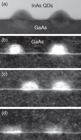
Figure 4.18 Cross‐sectional STEM images of size‐limited InAs QDs without (a) and with GaAs capping layers grown at 400 °C (b), 450 °C (c), and 500 °C (d).

Figure 4.19 A PL spectrum of size‐limited InAs QDs with GaAs capping layer grown under optimized conditions.
High‐density QDs are expected to improve the performance of semiconductor lasers and solar cells. In conventional SK growth of QDs, low growth temperatures, high arsenic pressures, and high growth rates of InAs/GaAs QDs yield high QD densities. However, high‐density QDs readily coalescence because of their proximity. Dislocations are often observed in the giant dots that result from such coalescence. Thus, coalescence must be suppressed to maintain a high crystal quality. An Sb‐mediated SK‐growth method using Sb‐containing underlying layers was employed to increase the density of InAs QDs and to suppress coalescence [28]. Figure 4.20 shows AFM images of high‐density InAs QDs grown on Sb/GaAs (a), GaAsSb/GaAs (b), and InAsSb/GaAs (c). The QD densities of (a), (b), and (c) were 1 × 1011 cm−2 [28], 5 × 1011 cm−2 [29], and 1 × 1012 cm−2 [30], respectively. There are no giant dots in this image; it is possible that the segregated Sb surface atoms suppressed QD coalescence. The high‐density InAs QDs on Sb/GaAs showed a narrow PL linewidth of about 28 meV [28]. Clearly, Sb‐mediated SK growth is a powerful method for obtaining high‐density, high‐uniformity InAs QDs with a high crystal quality.
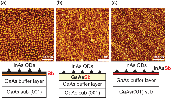
Figure 4.20 AFM images of high‐density InAs QDs grown on Sb/GaAs (a), GaAsSb/GaAs (b), and InAsSb/GaAs (c). QD densities of (a), (b), and (c) were 1 × 1011 cm−2, 5 × 1011 cm−2, and 1 × 1012 cm−2, respectively.
The self‐formation of in‐plane‐arranged QDs was attempted through a stacked growth technique or by using high‐index‐plane substrates. Strain control of the underlying buffer layers is one important technique for site control and the arrangement of QDs. The fabrication of 1D aligned InAs QD chains on GaAs(001) substrates is described below. The nucleation of 3D islands is related to the surface strain and surface undulation of the underlying buffer layers. Thus, strained buffer layers have been used for the selective growth of QDs. Figure 4.21(a) shows AFM images of InAs QDs on a GaAs(70–80 nm)/In0.16Ga0.84As(175 nm)/GaAs buffer layer. These InAs QDs were aligned periodically in the ![]() direction. The distance of periodicity between the QD chains ranged from 100 to 150 nm. The self‐formation of the QD chain structure can be attributed to misfit dislocations at the InGaAs/GaAs heterointerface [31]. Figure 4.21(b) shows a planar TEM image of InAs QD chains on a GaAs/InGaAs/GaAs buffer layer. The image reveals misfit dislocation lines at the upper GaAs/InGaAs heterointerface. No threading dislocations were observed in the buffer layer. Misfit dislocations were preferentially generated along the
direction. The distance of periodicity between the QD chains ranged from 100 to 150 nm. The self‐formation of the QD chain structure can be attributed to misfit dislocations at the InGaAs/GaAs heterointerface [31]. Figure 4.21(b) shows a planar TEM image of InAs QD chains on a GaAs/InGaAs/GaAs buffer layer. The image reveals misfit dislocation lines at the upper GaAs/InGaAs heterointerface. No threading dislocations were observed in the buffer layer. Misfit dislocations were preferentially generated along the ![]() direction, rather than the [110] direction, because of the anisotropic residual strain in the buffer layer. The
direction, rather than the [110] direction, because of the anisotropic residual strain in the buffer layer. The ![]() misfit dislocations were arranged in an orderly manner, and had a lateral spacing of about 100–150 nm. The lateral ordering of the misfit dislocations was mainly due to the periodic corrugation of the InGaAs layer. The periodic QD chains were aligned near the misfit dislocation lines along the
misfit dislocations were arranged in an orderly manner, and had a lateral spacing of about 100–150 nm. The lateral ordering of the misfit dislocations was mainly due to the periodic corrugation of the InGaAs layer. The periodic QD chains were aligned near the misfit dislocation lines along the ![]() direction. In addition, the number of QD chains was almost the same as the number of misfit dislocations. Thus, the self‐formation of periodic QD chains was presumably induced by the lateral ordering of misfit dislocations.
direction. In addition, the number of QD chains was almost the same as the number of misfit dislocations. Thus, the self‐formation of periodic QD chains was presumably induced by the lateral ordering of misfit dislocations.
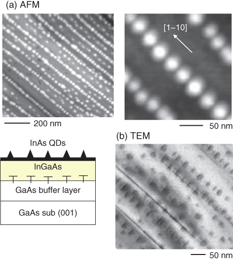
Figure 4.21 AFM images (a) and a planar TEM image (b) of InAs QD chains on a GaAs(70–80 nm)/In0.16Ga0.84As(175 nm)/GaAs buffer layer.
4.5 Conclusion
In this chapter, we reviewed the formation processes of semiconductor nanostructures (QWs, QWRs, NWRs, and QDs) by MBE. The fabrication of QW structures based on atomic‐level control of the thickness of heteroepitaxial layers and improving the flatness of the heterointerface is well established. In MBE growth, in‐situ RHEED observation is a powerful tool to control the epitaxial‐growth surface. By the epitaxial‐growth technique, many optoelectronic QW devices have already been developed. QWRs with an embedded layer are typically fabricated by epitaxial growth into V‐shaped grooves and on striped ridges or stepped surface structures, while NWRs are fabricated vertically or grown laterally on the substrates by VLS catalysis or selective‐area growth. Self‐assembled QDs were fabricated by SK‐mode growth. Uniform InAs QDs were achieved by the self‐size‐limiting effect. High‐density InAs QDs with narrow size distribution were formed by Sb‐mediated growth. Furthermore, 1D InAs QD chains were spontaneously formed along the ![]() direction on InGaAs/GaAs buffer layers. It is expected that as advances are made in the nanoepitaxial growth technique, QWRs, NWRs, and QDs will find application in nanophotonic and nanoelectronic devices with novel functions and good performance.
direction on InGaAs/GaAs buffer layers. It is expected that as advances are made in the nanoepitaxial growth technique, QWRs, NWRs, and QDs will find application in nanophotonic and nanoelectronic devices with novel functions and good performance.
References
- 1 Neave, J.H., Joyce, B.A., Dobson, P.I., and Norton, N. (1983). Appl. Phys. A31: 1.
- 2 Tanaka, M., Sakaki, H., and Yoshino, J. (1986). Jpn. J. Appl. Phys. 25: L155.
- 3 Neave, J.H., Dobson, P.I., and Joyce, B.A. (1985). Appl. Phys. Lett. 47: 100.
- 4 Gaines, J.M., Petroff, P.M., Kroemer, H. et al. (1988). J. Vac. Sci. Technol. B6: 1378.
- 5 Yuan, Z.L., Xu, Z.Y., Zheng, B.Z. et al. (1996). Phys. Rev. B54: 16919.
- 6 Wang, X.‐L. and Voliotis, V. (2006). Appl. Phys. Rev. 99: 121301.
- 7 Dasgupta, N.P., Sun, J., Liu, C. et al. (2014). Adv. Mater. 26: 2137.
- 8 Kapon, E., Hwang, D.M., and Bhat, R. (1989). Phys. Rev. Lett. 63: 430.
- 9 Haider, N., Wilby, M.R., and Vvedensky, D.D. (1993). Appl. Phys. Lett. 62: 3108.
- 10 Koshiba, S., Noge, H., Akiyama, H. et al. (1994). Appl. Phys. Lett. 64: 363.
- 11 Notzel, R., Ledentsov, N.N., Daweritz, L. et al. (1992). Phys. Rev. B45: 3507.
- 12 Higashiwaki, M., Yamamoto, M., Higuchi, T. et al. (1996). Jpn. J. Appl. Phys. 35: L606.
- 13 Wagner, R.S. and Ellis, W.C. (1964). Appl. Phys. Lett. 4: 89.
- 14 Tsai, C.T. and Williams, R.S. (1986). J. Mater. Res. 1: 352.
- 15 Dubrovskii, V.G., Cirlin, G.E., Soshnikov, I.P. et al. (2005). Phys. Rev. B71: 205325.
- 16 Colombo, C., Spirkoska, D., Frimmer, M. et al. (2008). Phys. Rev. B77: 155326.
- 17 Schumann, T., Gotschke, T., Limbach, F. et al. (2011). Nanotechnology 22: 095603.
- 18 Goldstein, L., Glas, F., Marzin, J.Y. et al. Appl. Phys. Lett. 41: 1099, 1985.
- 19 Koguchi, N., Takahashi, S., and Chikyow, T. (1991). J. Cryst. Growth 111: 688.
- 20 Eaglesham, D.J. and Cerullo, M. (1990). Phys. Rev. Lett. 4: 1943.
- 21 Marti Ceschin, A. and Massies, J. (1991). J. Cryst. Growth 114: 693.
- 22 Yamaguchi, K., Kaizu, T., Yujobo, K., and Saito, Y. (2002). J. Cryst. Growth 237–239: 1301.
- 23 Murray, R., Childs, D., Malik, S. et al. (1999). Jpn. J. Appl. Phys. 38: 528.
- 24 Yamaguchi, K., Yujobo, K., and Kaizu, T. (2000). Jpn. J. Appl. Phys. 39: L1245.
- 25 Kaizu, T. and Yamaguchi, K. (2003). Jpn. J. Appl. Phys. 42: 4166.
- 26 Barabási, A.‐L. (1997). Appl. Phys. Lett. 70: 2565.
- 27 García, J.M., Medeiros‐Ribeiro, G., Schmidt, K. et al. (1997). Appl. Phys. Lett. 71: 2014.
- 28 Yamaguchi, K. and Kanto, T. (2005). J. Cryst. Growth 275: e2269.
- 29 Saputra, E., Ohta, J., Kakuda, N., and Yamaguchi, K. (2012). Appl. Phys. Express 5: 125502.
- 30 Sameshima, K., Sano, T., and Yamaguchi, K. (2016). Appl. Phys. Express 9: 075501.
- 31 Yamaguchi, K., Waki, E., and Hasegawa, H. (1997). Jpn. J. Appl. Phys. 36: L871.